

Datasheet AT49F2048-90TI, AT49F2048-90TC, AT49F2048-90RI, AT49F2048-90RC, AT49F2048-70TI Datasheet (ATMEL)
...Page 1
Features
Single Voltage Operation
•
– 5V Read
– 5V Reprogramming
Fast Read Access Time - 70 ns
•
Internal Erase/Program Control
•
Sector Architecture
•
– One 8K Words (16K bytes) Boot Block with Programming Lockout
– Two 8K Words (16K bytes) Parameter Blocks
– One 104K Words (208K bytes) Main Memory Array Block
Fast Sector Erase Time - 10 seconds
•
Word-By-Word Programming - 50 µs/Word
•
Hardware Data Protection
•
DAT A Polling For End Of Program Detection
•
Low Power Dissipation
•
– 50 mA Active Current
– 300 µA CMOS Standby Current
Typical 10,000 Write Cycles
•
2-Megabit
(128K x 16)
5-volt Only
CMOS Flash
Description
The AT49F2048 is a 5-volt-only, 2 megabit Flash Memory organized as 128K words
of 16 bits each. Manufactured with Atmel's advanced nonvolatile CMOS technology,
the device offers access times to 70 ns with pow er dissipati on of just 275 mW. Wh en
deselected, the CMOS standby current is less than 300 µA.
To allow for simple in-system reprogrammability, the AT49F2048 does not require
high input voltages for programming. Five-volt-only commands determine the read
and programming operation of the device. Reading data out of the device is similar to
(continued)
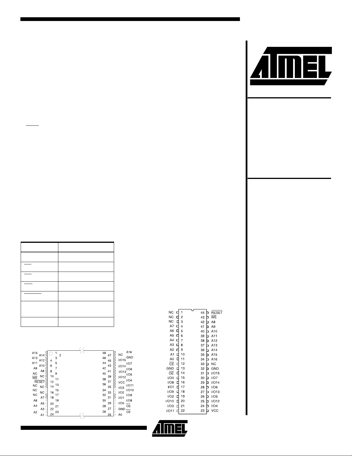
Pin Configurations
Pin Name Function
A0 - A16 Addresses
CE
OE Output Enable
WE
RESET
I/O0 - I/O15
NC No Connect
Chip Enable
Write Enable
Reset
Data
Inputs/Outputs
TSOP Top View
Type 1
SOIC (SOP)
Memory
AT49F2048
0568D-A–9/97
1
Page 2
reading from an E PROM ; it h as stan dard CE
inputs to avoid bus connection. The AT49F2048 is a 5-voltonly, 2 megabit Flash Memory organized as 128K words
contention. Reprogramm ing the AT49F 2048 is performed
by first erasing a b lock of data an d then program ming o n a
word-by-word basis.
The device is erased by executing the erase command
sequence; the device internally controls the erase operation. The memory is di vided into three bl ocks for erase
operations. There are two 8K word parameter block sections and one sector consisting of the boot block and the
main memory array b lock . The AT4 9F2048 i s program med
on a word-by-word basis.
, OE, and WE
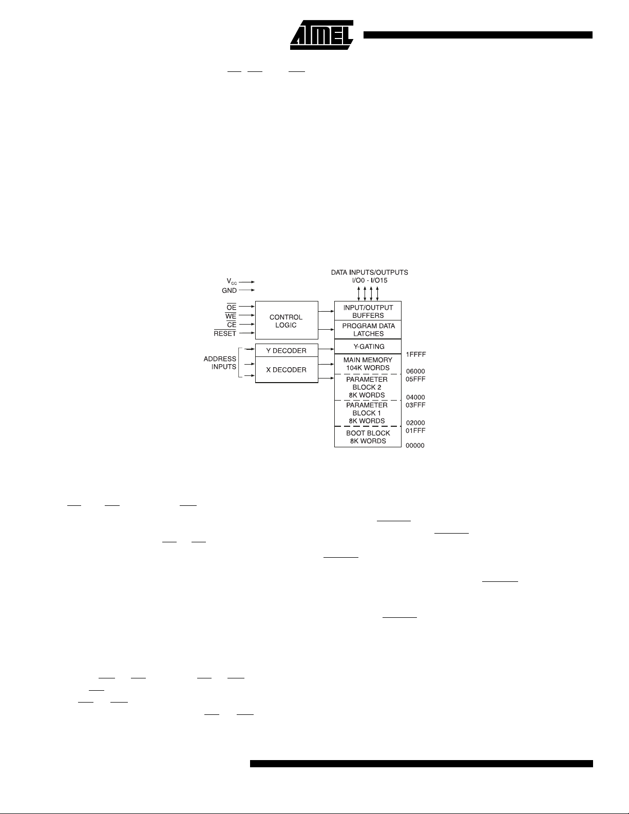
Block Diagram
The device has the capability to protect the data in the boot
block; this feature is enabled by a command sequence.
Once the boot block programming lockout feature is
enabled, the data in the boot bl ock cannot be cha nged
when input levels of 5.5 volts or less are used. The typical
number of program and erase cycles is in excess of 10,000
cycles.
The optional 8K word boot block section includes a reprogramming lock o ut featur e to pro vide data i ntegrity. The
boot sector is des igned to contain us er secure code, and
when the feature is enabled, the boot sector is protected
from being reprogrammed.
Device Operation
READ:
When CE
at the memory location determined by the address pins is
asserted on the outputs . The outputs ar e put in the high
impedance state whenever CE
control gives designers flexibility in preventing bus contention.
COMMAND SEQUENCES:
ered on it will be reset to the read or standby mode
depending upon the state of the control line inputs. In order
to perform other device functions, a series of command
sequences are entered into the device. The command
sequences are shown in the Comma nd Definitions ta ble
(I/O8 - I/O15 are don't care inputs for the command codes).
The command sequences are written by applying a low
pulse on the WE
tively) and OE
edge of CE
latched by the first rising ed ge of CE
microprocessor write timings are used. T he address loc a-
2
The AT49F2048 is accessed like an EPROM .
and OE are low and WE is high, th e data sto red
or OE is high. This dual-line
When the device is first pow-
or CE input with CE or WE low ( respec-
high. The addre ss is latche d on the fall ing
or WE, whichever occurs last. The data is
or WE. Standard
AT49F2048
tions used in the command sequences are not affected by
entering the command sequences.
RESET:
tem applications. When RESET
device is in its sta nda rd ope ra tin g mo de. A lo w level on the
RESET
the outputs of the de vice in a hig h impeda nce sta te. When
a high level is reas serted on the RESE T
returns to the Read or Standby mo de, dependi ng upon the
state of the control inputs. By applying a 12V ± 0.5V input
signal to the RE SE T
grammed even if the boot block program lockout feature
has been enabled (see Boot Block Pro gramming Loc kout
Override section).
ERASURE:
be erased. The erased state of the memory bits is a logical
“1”. The entire device can be erased at one time by using a
6-byte software code.
A RESET
input halts the pre sent d evice o perati on and puts
Before a word can be reprogrammed, it must
input pin is provided to eas e some sys-
is at a l ogic high le ve l, t he
pin, the device
pin the boot block array can be repro -
Page 3

AT49F2048
After the software chip erase has been ini tiated , the devi ce
will internally time the eras e operatio n so that no ex ternal
clocks are required. The maximum time needed to erase
the whole chip is t
CHIP ERASE:
the Chip Erase function is disabled; sector erases for the
parameter blocks a nd ma in me mory b lock will s till op erate .
After the full chip erase the device will return back to read
mode. Any command during chip erase will be ignored.
SECTOR ERASE:
the device is organized into three sectors that can be individually erased. There are two 8K word parameter block
sections and one sector consisting of the boot block and
the main memory array blo ck. The Secto r Erase comm and
is a six bus cycle operation. The sector address is latched
on the falling WE
input command is latched at the rising edge of WE
sector erase starts after the rising edge of WE
cycle. The erase oper ation is internal ly controlled; it will
automatically time to c omple tion. W hen the b oot block programming lockout featur e is not enabled, the boot block
and the main memory block will erase together (from the
same sector erase command). Once the boot region has
been protected, only the main memory array sector will
erase when its sector erase command is issued.
WORD PROGRAMMING:
erased, it is programmed (to a logical “0”) on a word-byword basis. Programming is accomplished via the internal
device command register and is a 4 bus cycle operation.
The device will autom ati ca ll y ge nerate the required inter nal
program pulses.
Any commands written to the chip during the embedded
programming cycle will be ignored. If a hardware reset happens during programming, the data at the location being
programmed will be corrupted. Please note that a data “0”
cannot be programmed back to a “1”; only erase operations
can convert “0”s to “1”s. Programming is completed after
the specified tBP cycle time. The DATA
also be used to indicate the end of a program cycle.
BOOT BLOCK PROGRAMMING L OCKOUT:
has one designated block that has a programming lockout
feature. This feature prevents programmi ng of data in the
designated block once the feature has been enabled. The
size of the block is 8K wo rds. This bl ock, referr ed to as the
boot block, ca n conta in se cure code th at is used to brin g up
the system. Enablin g the l ockout fe ature will all ow the boot
code to stay in the device while data in the rest of the
device is updated. This feature does not have to be activated; the boot blo ck' s usage as a wr it e protected region is
optional to the user. The address range of the boot block is
00000H to 01FFFH.
Once the feature is enabled, the data in the boot block can
no longer be erased or programmed when input levels of
.
EC
If the boot block lockout has bee n en abl ed ,
As an alternative to a full chip erase,
edge of the sixth cycle while the 30H data
. The
of the si xth
Once a memory block is
polling feature may
The device
5.5V or less are u sed. Dat a in the m ain mem ory bloc k can
still be changed through the regular programming method.
To activate the lockout feature, a series of six program
commands to specific addresses with specific data must be
performed. Please refer to the Command Definitions table.
BOOT BLOCK LOCKOUT DETECTION:
method is available to determine if programming of the boot
block section is locked out. When the device is in the software product identification mode (see Software Product
Identification Entry and Exit sections) a read from address
location 00002H wil l s how i f pr ogram mi ng the b oot block is
locked out. If the data on I/O0 is low, the boot bl oc k c an be
programmed; if the data on I/O0 is high, the program lockout feature has been enabled and the bl ock ca nnot be programmed. The software product identification exit code
should be used to return to standard operation.
BOOT BLOCK PROGRAMMING LOCKOUT OVERRIDE:
The user can override the boot block programming
lockout by taking the RESET
protected boot bl ock data can be altered throug h a chip
erase, sector erase or word programm ing. When the
RESET
programming lockout feature is again active.
PRODUCT IDENTIFICATION:
mode identifies the device and manufacturer as Atmel. It
may be accessed by hardware or software operation. The
hardware operation mode can be used by an external programmer to identify the correct programming algorithm for
the Atmel product.
For details, see Operating Modes (for hardware operation)
or Software Product Identification. The manufacturer and
device code is the same for both modes.
DATA POLLING:
to indicate the end of a pr ogram cy cle. Duri ng a progr am
cycle an attempted read of the last byte loaded will result in
the complement of the loaded data on I/O7. Once the program cycle has been comp leted, true data is valid on all
outputs and the next cycle may begin. During a chip or sector erase operation , an atte mpt to rea d the devi ce will g ive
a “0” on I/O7. Once the program or erase cycle has completed, true data will be read from the device. DATA
may begin at any time during the program cycle.
TOGGLE BIT:
provides another method for determining the end of a program or erase cycle. During a pro gram or er ase opera tion,
successive attempts to read data from the device will result
in I/O6 toggling between one and zero. Once the program
cycle has completed, I/O6 will stop toggling and valid data
will be read. Examining the toggle bit may begin at any time
during a program cycle.
HARDWARE DATA PROTECTION:
protect against inadvertent programs to the AT49F2048 in
the following ways: (a) V
pin is broug ht back to TTL lev els the bo ot block
The AT49F2048 features DATA
In addition to DATA
pin to 12 volts. By doing this
The product identif ication
polling the AT49F2 048
Hardware features
sense: if VCC is below 3.8V
CC
A software
polling
polling
3
Page 4
(typical), the prog ram func tion is inhi bited. (b) V
on delay: once V
has reached the VCC sense level, the
CC
CC
power
device will automatically time out 10 ms (typical) before
programming. (c) Program inhibit: holding any one of OE
low, CE high or W E high inhib its prog ram cy cles. ( d) Noise
filter: pulses of les s than 15 ns (typ ical) on the W E
or CE
inputs will not initiate a program cycle.
OUT
(1)
2nd Bus
Cycle
3rd Bus
Cycle
4th Bus
Cycle
5th Bus
Cycle
IN
6th Bus
Cycle
(4)(5)
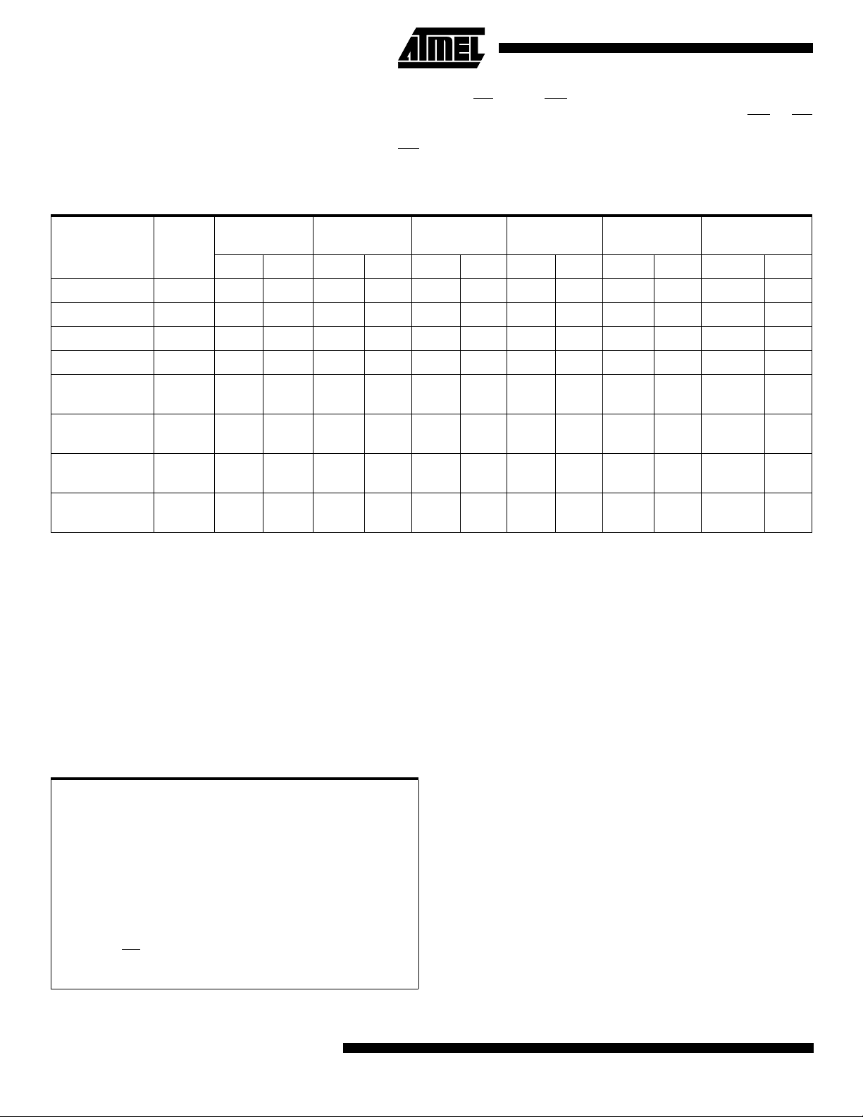
Command Definition (in Hex)
1st Bus
Command
Sequence
Read 1 Addr D
Chip Erase 6 5555 AA 2AAA 55 5555 80 5555 AA 2AAA 55 5555 10
Sector Erase 6 5555 AA 2AAA 55 5555 80 5555 AA 2AAA 55 SA
Word Program 4 5555 AA 2AAA 55 5555 A0 Addr D
Boot Block
Lockout
Product ID
Entry
Product ID
Exit
Product ID
Exit
Notes: 1. The DATA FORMAT in each bus cycle is as follows: I/O15 - I/O8 (Don't Care); I/O7 - I/O0 (Hex)
(2)
(3)
(3)
2. The 8K word boot sector has the address range 00000H to 01FFFH.
3. Either one of the Product ID Exit commands can be used.
4. SA = sector addresses:
SA = 03XXX for PARAMETER BLOCK 1
SA = 05XXX for PARAMETER BLOCK 2
SA = 1FXXX for MAIN MEMORY ARRAY
5. When the boot block programming lockout feature is not enabled, the boot block and the main memory block will erase
together (from the same sector erase command). Once the boot region has been protected, only the main memory array
sector will erase when its sector erase command is issued.
Bus
Cycles
6 5555 AA 2AAA 55 5555 80 5555 AA 2AAA 55 5555 40
3 5555 AA 2AAA 55 5555 90
3 5555 AA 2AAA 55 5555 F0
1xxxxF0
Cycle
Addr Data Addr Data Addr Data Addr Data Addr Data Addr Data
30
Absolute Maximum Ratings*
Temperature Under Bias................................ -55°C to +125°C
Storage Temperature..................................... -65°C to +150°C
All Input Voltages
(including NC Pins)
with Respect to Ground...................................-0.6V to +6.25V
All Output Voltages
with Respect to Ground............................-0.6V to V
Voltage on OE
with Respect to Ground...................................-0.6V to +13.5V
4
AT49F2048
+ 0.6V
CC
*NOTICE: Stresses beyond those listed under “Absolute
Maximum Ratings” may cause permanent damage to the dev ice . This is a s tress rating only an d
functional oper ation of the device at thes e o r any
other conditions beyond those indicated in the
operational sections of this specification is not
implied. Exposure to absolute maximum rating
conditions f or e xtended periods ma y af fect de vice
reliability .
Page 5

AT49F2048
DC and AC Operating Range
AT49F2048-70 AT49F2048-90 AT49F2048-12
Operating
Temperature (Case)
V
Power Supply 5V ± 10% 5V ± 10% 5V ± 10%
CC
Operating Modes
Mode CE OE WE RESET Ai I/O
Read V
Program/Erase
Standby/Write Inhibit V
Program Inhibit X X V
Program Inhibit X V
Output Disable X V
Reset X X X V
Product Identification
Hardware V
Software
Notes: 1. X can be VIL or VIH.
(2)
(5)
2. Refer to AC Programming Waveforms.
= 12.0V ± 0.5V.
3. V
H
4. Manufacturer Code: 1FH, Device Code: 82H
5. See details under Software Product Identification Entry/Exit.
Com. 0°C - 70°C 0°C - 70°C 0°C - 70°C
Ind. -40°C - 85°C -40°C - 85°C -40°C - 85°C
V
X
V
V
IL
IH
IL
IH
IL
IL
V
IL
IH
IL
V
IH
V
IL
(1)
XV
IH
XV
XV
V
IH
V
IH
V
IH
IH
V
IH
IH
IH
IL
A1 - A16 = VIL, A9 = VH,
V
IH
V
IH
A1 - A16 = VIL, A9 = VH,
A0 = VIL, A1 - A16 = V
A0 = VIH, A1 - A16 = V
Ai D
Ai D
X High Z
X High Z
(3)
A0 = V
IL
(3)
A0 = V
IH
IL
IL
OUT
IN
High Z
Manufacturer Code
Device Code
Manufacturer Code
Device Code
(4)
(4)
(4)
(4)
DC Characteristics
Symbol Parameter Condition Min Max Units
I
LI
I
LO
I
SB1
I
SB2
(1)
I
CC
V
IL
V
IH
V
OL
V
OH1
V
OH2
Note: 1. In the erase mo de, I
Input Load Current VIN = 0V to V
Output Leakage Current V
= 0V to V
I/O
CC
CC
VCC Standby Current CMOS CE = VCC - 0.3V to V
VCC Standby Current TTL CE = 2.0V to V
V
Active Current f = 5 MHz; I
CC
CC
= 0 mA 50 mA
OUT
CC
10
10
300
3mA
Input Low V oltage 0.8 V
Input High Voltage 2.0 V
Output Low Voltage IOL = 2.1 mA .45 V
Output High Voltage IOH = -400 µA2.4V
Output High Voltage CMOS IOH = -100 µA; VCC = 4.5V 4.2 V
is 90 mA.
CC
µ
A
µ
A
µ
A
5
Page 6

AC Read Characteristics
Symbol Parameter
t
ACC
t
CE
t
OE
t
DF
t
OH
(1)
(2)
(3)(4)
Address to Output Delay 70 90 120 ns
CE to Output Delay 70 90 120 ns
OE to Output Delay 35 0 40 0 50 ns
CE or OE to Output Float 0 25 0 25 0 30 ns
Output Hold from OE, CE
or Address, whichever occurred first
AT49F2048-70 AT49F2048-90 AT49F2048-12
UnitsMin Max Min Max Min Max
000ns
AC Read Waveforms
(1)(2)(3)(4)
ADDRESS
OUTPUT
Notes: 1. CE may be delayed up to t
2. OE
3. tDF is specified from OE or CE whichever occurs first (CL = 5 pF).
4. This parameter is characterized and is not 100% tested.
may be delayed up to t
change without impact on t
ADDRESS VALID
CE
t
CE
t
t
ACC
OE
OUTPUT
t
OH
t
DF
OE
HIGH Z
VALID
- tCE after the address transition without impact on t
ACC
- tOE after the falling edge of CE without impact on tCE or by t
CE
.
ACC
ACC
.
- tOE after an address
ACC
Output Test LoadInput Test Wa veforms and Measurement Level
tR, tF < 5 ns
Pin Capacitance
(f = 1 MHz, T = 25°C)
C
IN
C
OUT
Note: 1. This parameter is character i zed and is not 100% tested.
6
(1)
Typ Max Units Conditions
46 pF V
812 pF V
AT49F2048
IN
OUT
= 0V
= 0V
Page 7

AT49F2048
AC Word Load Characteristics
Symbol P arameter Min Max Units
t
, t
AS
t
AH
t
CS
t
CH
t
WP
t
DS
t
, t
DH
t
WPH
AC Word Load Waveforms
WE Controlled
Address, OE Set-up Time 10 ns
OES
Address Hold Time 50 ns
Chip Select Set-up Time 0ns
Chip Select Hold Time 0ns
Write Pulse Width (WE or CE) 100 ns
Data Set-up Time 50 ns
Data, OE Hold Time 10 ns
OEH
Write Pulse Width High 100 ns
OE
CE
Controlled
ADDRESS
CE
WE
DATA IN
OE
ADDRESS
WE
t
t
t
AS
CS
AS
t
OES
t
OES
t
t
AH
AH
t
t
DS
WP
t
OEH
t
CH
t
WPH
t
DH
t
OEH
t
CH
CE
DATA IN
t
CS
t
t
DS
WP
t
WPH
t
DH
7
Page 8

Program Cyc le Characteristics
Symbol Parameter Min Max Units
t
BP
t
AS
t
AH
t
DS
t
DH
t
WP
t
WPH
t
EC
Word Programming Time 50 µs
Address Set-up Time 10 ns
Address Hold Time 50 ns
Data Set-u p Time 50 ns
Data Hold Time 10 ns
Write Pulse Width 100 ns
Write Pulse Width High 100 ns
Erase Cycle Time 10 seconds
Program Cycle Waveforms
PROGRAM CYCLE
OE
CE
t
BP
5555
AA
WE
A0-A16
DATA
t
WP
t
AS
5555 2AAA 5555
t
AH
t
DS
AA 55 A0
t
WPH
t
DH
ADDRESS
INPUT
DATA
Sector or Chip Erase Cycle Waveforms
(1)
OE
CE
t
WP
WE
t
AH
t
DS
AA 55 80
WORD 0 WORD 1 WORD 2 WORD 3 WORD 4 WORD 5
A0-A16
DATA
t
AS
5555 2AAA 5555
Notes: 1. OE must be high only when WE and CE are both low.
2. For chip erase, the address should be 5555. For sector erase, the address depends on what sector is to be erased. (See
note 4 under command definitions.)
3. For chip erase, the data should be 10
8
AT49F2048
, and for sector erase, the data should be 30H.
H
t
WPH
t
DH
5555 2AAA Note 2
AA 55 Note 3
t
EC
Page 9

AT49F2048
Data Polling Characteristics
(1)
Symbol Parameter Min Typ Max Units
t
DH
t
OEH
t
OE
t
WR
Data Hold Time 10 ns
OE Hold Time 10 ns
OE to Output Delay
(2)
Write Recovery Time 0 ns
Notes: 1. These parameters are characterized and not 100% tested.
2. See tOE spec in AC Read Characteristics.
Data Polling Waveforms
WE
CE
t
OEH
OE
I/O7
A0-A16
t
DH
t
OE
HIGH Z
An
An An AnAn
t
WR
ns
Toggle Bit Characteristics
(1)
Symbol Parameter Min Typ Max Units
t
DH
t
OEH
t
OE
t
OEHP
t
WR
Data Hold Time 10 ns
OE Hold Time 10 ns
OE to Output Delay
(2)
OE High Pulse 150 ns
Write Recovery Time 0 ns
Notes: 1. These parameters are characterized and not 100% tested.
2. See tOE spec in AC Read Characteristics.
Toggle Bit Waveforms
(1)(2)(3)
WE
CE
OE
I/O6
t
t
DH
OEH
t
OEHP
t
OE
HIGH Z
t
WR
ns
Notes: 1. Toggling either OE or CE or both OE and CE will operate toggle bit. The t
input(s).
2. Beginning and ending state of I/O6 will vary.
3. Any address location may be used but the address should not vary.
specification must be met by the toggling
OEHP
9
Page 10

Software Product
LOAD DATA AA
TO
ADDRESS 5555
LOAD DATA 55
TO
ADDRESS 2AAA
LOAD DATA 80
TO
ADDRESS 5555
LOAD DATA AA
TO
ADDRESS 5555
LOAD DATA 55
TO
ADDRESS 2AAA
LOAD DATA 40
TO
ADDRESS 5555
PAUSE 1 second
Identification Entry
LOAD DATA AA
ADDRESS 5555
LOAD DATA 55
ADDRESS 2AAA
LOAD DATA 90
ADDRESS 5555
ENTER PRODUCT
IDENTIFICATION
MODE
(1)
TO
TO
TO
(2)(3)(5)
Boot Block Lockou t
Enable Algorithm
(1)
Software Product
.
IL
(1)(6)
OR
Identification Exit
LOAD DATA AA
TO
ADDRESS 5555
LOAD DATA 55
TO
ADDRESS 2AAA
LOAD DATA F0
TO
ADDRESS 5555
EXIT PRODUCT
IDENTIFICATION
Notes: 1. Data Format: I/O15 - I/O8 (Don’t Care);
(4)
MODE
I/O7 - I/O0 (Hex)
Address Format: A14 - A0 (Hex).
2. A1 - A16 = V
Manufacture Code is read for A0 = V
Device Code is read for A0 = V
3. The device does not remain in identification mode if
powered down.
4. The device returns to standard operation mode.
5. Manufacturer Code: 1FH
Device Code: 82H
6. Either one of the Product ID Exit commands can be
used.
LOAD DATA F0
TO
ANY ADDRESS
EXIT PRODUCT
IDENTIFICATION
IH
MODE
IL
.
(4)
;
Notes: 1. Data Format: I/O15 - I/O8 (Don’t Care);
I/O7 - I/O0 (Hex)
Address Format: A14 - A0 (Hex).
2. Boot block lockout feature enabled.
10
AT49F2048
Page 11

AT49F2048
Ordering Information
t
ACC
(ns)
70 50 0.3 AT49F2048-70RC
90 50 0.3 AT49F2048-90RC
120 50 0.3 AT49F2048-12RC
Note: 1. The AT49F2048 has as optional boot block feature. The part number shown in the Ordering Information table is for devices
with the boot block in the lower address range (i.e., 00000H to 01FFFH). Users requiring the boot block to be in the higher
address range should contac t Atmel.
ICC (mA)
50 0.3 AT49F2048-70RI
50 0.3 AT49F2048-90RI
50 0.3 AT49F2048-12RI
(1)
Ordering Code Packa ge Operation RangeActive Standby
AT49F2048-70TC
AT49F2048-70TI
AT49F2048-90TC
AT49F2048-90TI
AT49F2048-12TC
AT49F2048-12TI
44R
48T
44R
48T
44R
48T
44R
48T
44R
48T
44R
48T
Commercial
(0° to 70°C)
Industrial
(-40° to 85°C)
Commercial
(0° to 70°C)
Industrial
(-40° to 85°C)
Commercial
(0° to 70°C)
Industrial
(-40° to 85°C)
Package Type
44R 44-Lead, 0.525" Wide, Plastic Gull-Wing Small Outline Package (SOIC/SOP)
48T 48-Lead, Thin Small Outline Package (TSOP)
11
 Loading...