

Datasheet AT49F1025-90VI, AT49F1025-90VC, AT49F1025-90JI, AT49F1025-90JC, AT49F1025-70VI Datasheet (ATMEL)
...Page 1
Features
Single Voltage Operation
•
– 5V Read
– 5V Reprogramming
Fast Read Access Time - 45 ns
•
Internal Program Control and Timer
•
8K word Boot Block With Lockout
•
Fast Erase Cycle Time - 10 seconds
•
Word By Word Programming - 10
•
Hardware Data Protection
•
DAT A Polling For End Of Program Detection
•
Small 10 x 14 mm VSOP Package
•
Typical 10,000 Write Cycles
•
µµµµ
s/Word Typical
1-Megabit
(64K x 16)
Description
The AT49F1024 and the AT49F1025 ar e 5-v olt -o nly in -sy stem Fla sh Mem or ies . The ir
1 megabit of memory is organized as 65,536 words by 16 bits. Manufactured with
Atmel’s advanced nonvolatile CMOS technology, the devices offer access times to 45
ns with power dissipation of just 275 mW over the commercial temperature range.
When the device is deselected, the CMOS standby current is less than 100 µA. The
only differenc e between th e AT49F1024 and the AT4 9F1025 is th e pinout. T he
AT49F1024 is pin compatable with the AT27C1024, and the AT49F1025 is pin compatable with the AT29C1024.
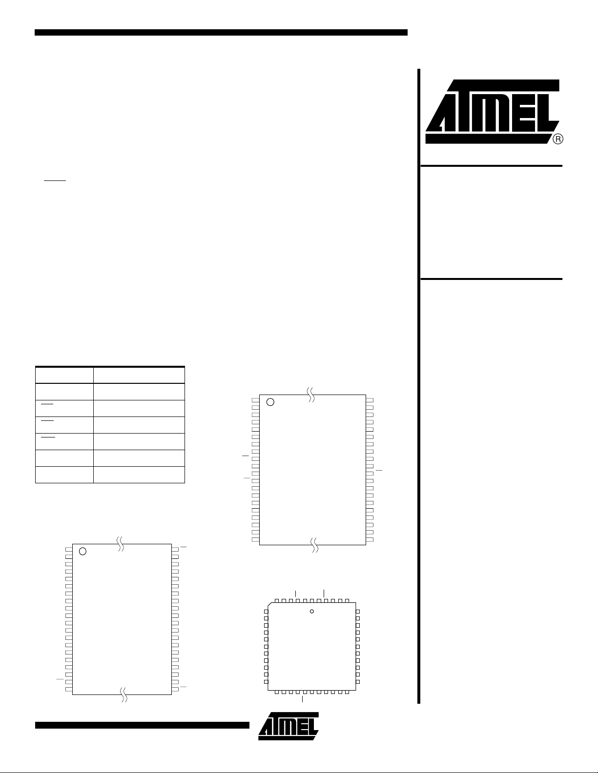
Pin Configurations
Pin Name Function
A0 - A15 Addresses
CE
OE Output Enable
WE
I/O0 - I/O15 Data Inputs/Outputs
NC No Connect
AT49F1025 VSOP Top View
A0
A1
A2
A3
A4
A5
A6
A7
A8
GND
A9
A10
A11
A12
A13
A14
A15
NC
WE
VCC
1
2
3
4
5
6
7
8
9
10
11
12
13
14
15
16
17
18
19
20
Chip Enable
Write Enable
Type 1
10 x 14 mm
10 x 14 mm
AT49F1024 VSOP Top View
Type 1
10 x 14 mm
1
A9
2
A10
3
A11
4
A12
5
A13
6
A14
7
A15
8
NC
9
WE
10
VCC
11
NC
12
CE
13
I/O15
14
I/O14
15
I/O13
16
I/O12
17
I/O11
18
I/O10
19
I/O9
20
I/O8
40
OE
39
I/O0
38
I/O1
37
I/O2
36
I/O3
35
I/O4
34
I/O5
33
I/O6
32
I/07
31
GND
30
I/O8
29
I/O9
28
I/O10
27
I/O11
26
I/O12
25
I/O13
24
I/O14
23
I/O15
22
NC
21
CE
I/O12
I/O11
I/O10
GND
PLCC Top View
I/O13
I/O14
I/O15CENCNCVCCWENC
65432
7
8
9
10
I/O9
11
I/O8
12
13
NC
14
I/O7
15
I/O6
16
I/O5
17
I/O4
1819202122232425262728
I/O3
I/O2
I/O1
I/O0
1
OE
DC
4443424140
A0A1A2A3A4
(continued)
40
39
38
37
36
35
34
33
32
31
30
29
28
27
26
25
24
23
22
21
A15
A14
39
A13
38
A12
37
A11
36
A10
35
A9
34
GND
33
NC
32
A8
31
A7
30
A6
29
A5
GND
A8
A7
A6
A5
A4
A3
A2
A1
A0
OE
I/O0
I/O1
I/O2
I/O3
I/O4
I/O5
I/O6
I/O7
GND
5-volt Only
Flash Memory
AT49F1024
AT49F1025
Rev. 0765D–09/98
1
Page 2
To allow for simple in-system reprogrammability, the
AT49F1024/1025 does not requir e high input voltage s for
programming. Five-volt-only commands determine the read
and programming operation of the device. Reading data
out of the device is similar to reading from an EPROM.
Reprogramming the AT49F1024 /1025 is performed by
erasing a block of da ta (entir e chip or ma in memo ry block)
and then programming on a word by word basis. The typical word programming time is a fast 10 µs. The end of a
program cycle can be optionally detected by the DATA
poll-
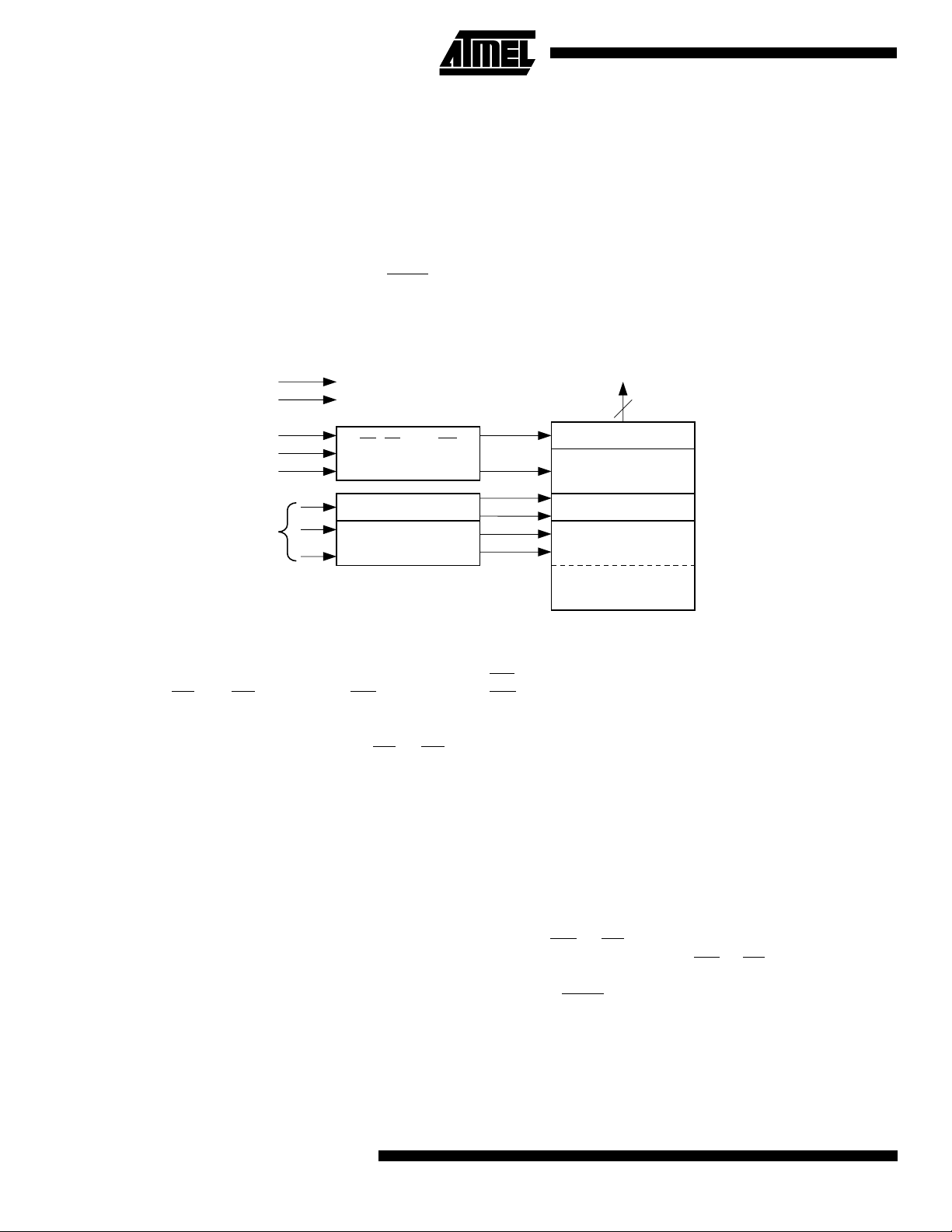
Block Diagram
V
CC
GND
ing feature. Once the end of a byte program cycle has been
detected, a new access for a read or program can begin.
The typical number of program and erase cycles is in
excess of 10,000 cycles.
The optional 8K words boot block section in clude s a reprogramming write lock out feature to provide data integrity.
The boot sector is designed to contain user secure code,
and when the featur e is en abled, the bo ot sec tor is per manently protected from being erased or reprogrammed.
DATA INPUTS/OUTPUTS
I/O15 - I/O0
16
OE
WE
CE
ADDRESS
INPUTS
OE, CE, AND WE
LOGIC
Y DECODER
X DECODER
Device Operation
READ:
EPROM. When CE
data stored at the memory location determined by the
address pins is asserted on the outputs. The outputs are
put in the high impedance state whenever CE
high. This dual-line con tr ol gi v es d esign er s fl ex ibi lit y in pr eventing bus contention.
CHIP ERASE:
feature is not enabled, the boot block and the main memory
block will erase together from the same chip erase command (See command definitions table). If the boot bl ock
lockout function has been enabled, data in the boot section
will not be erased. Howe ver, data in the main mem or y se ction will be erased. After a chip erase, the device will return
to the read mode.
MAIN MEMORY ERASE:
erase, a main memory block erase can be performed which
will erase all bytes not located in the boot block region to an
FFH. Data located in the boot region will not be changed
during a main memory block erase. The Main Memory
Erase command is a six bus cycle operation. The address
(5555H) is latched on the falling edge of the sixth cycle
while the 30H data input is latche d on the rising edge of
The AT49F1024/10 25 is accessed like an
and OE are low and WE is high, th e
or OE is
When the boot block programming lockout
As an alternative to the chip
DATA LATCH
INPUT/OUTPUT
BUFFERS
Y-GATING
MAIN MEMORY
(56K WORDS)
OPTIONAL BOOT
BLOCK (8K WORDS)
. The main memory erase starts aft er the risi ng edge of
WE
of the sixth cycle. P lease see Main Mem ory Erase
WE
1FFFH
0000H
cycle waveforms. The Main Memory Erase operation is
internally controlled; it will automatically time to completion.
WORD PROGRAMMING:
Once the memory array is
erased, the device is programmed (to a logical “0”) on a
word-by-word basis. Please note that a data “0” cannot be
programmed back to a “1”; only erase operations can convert “0”s to “1”s. Programming is accomplished via the
internal device command register and is a 4 bus cycle
operation (please refer to the Command Definitions table).
The device will automatic ally gen erate the required internal
program pulses.
The program cyc le has address es latched on the falling
edge of WE
latched on the rising edge of WE
first. Programming is completed after the specified t
time. The DATA
or CE, whichever occurs last, and the data
or CE, whichever occurs
cycle
BP
polling feature may also be us ed to indi-
cate the end of a program cycle.
BOOT BLOCK PROGRAMMING LOCKOUT:
The device
has one designated block that has a programming lockout
feature. This feature prevents programming of data in th e
designated block once the feature has been enabled. The
2
AT49F1024/1025
Page 3

AT49F1024/1025
size of the block is 8K words. Thi s blo ck, refe rred to as th e
boot block, can contain secure code that is used to bring up
the system. Enablin g the lo ckou t featur e will al low the boot
code to stay in the device while data in the rest of the
device is updated. This feature does not have to be activated; the boot block’s us ag e as a wr i te protected region is
optional to the user. The address range of the boot block is
0000H to 1FFFH.
Once the feature is enabled, the data in th e boot blo ck ca n
no longer be erased or programmed. Data in the main
memory block can still be changed through the regular programming method and can be er ased using ei ther the chip
erase or the main memory block erase command. To activate the lockout feature, a series of six program commands
to specific addresses with specific data must be performed.
Please refer to the Command Definitions table.
BOOT BLOCK LOCKOUT DETECTION:
method is available to determine if programming of the boot
block section is locked out. When the device is in the software product ident ification mode (s ee Software Produ ct
Identification Entry and Exit sections) a read from address
location 0002H will show if programming the boot block is
locked out. If the da ta o n I/O0 is low, the boot block can be
programmed; if the data on I/O0 is high, the program lockout feature has been activated and the block cannot be
programmed. The software product identification exit code
should be used to return to standard operation.
PRODUCT IDENTIFICATION:
mode identifies the device and manufacturer as Atmel. It
may be accessed by hardware or software operation. The
hardware operation mode can be used by an external pro-
The product identificatio n
A software
grammer to identify the correct programming algorithm for
the Atmel product.
For details, see O perat ing Mode s (for ha rdware operat ion)
or Software Product Identification. The manufacturer and
device code is the same for both modes.
DATA POLLING:
polling to indicate the end of a program or erase cycle.
During a program cycle an attempted read of the last byte
loaded will result in the complement of the loaded data on
I/O7. Once the program cycle has been completed, true
data is valid on all output s and the nex t cycle ma y begin.
polling may begi n at any time during the pr ogram
DATA
cycle.
TOGGLE BIT:
AT49F1024/1025 provides anothe r method for determi ning
the end of a program or erase cycle. During a program or
erase operation, successive attempts to read data from the
device will result in I/O6 toggling between one and zero.
Once the program cycle has completed, I/O6 will stop toggling and valid data will be read. Exami ning the to ggle bit
may begin at any time during a program cycle.
HARDWARE DATA PROTECTION:
protect against inadvertent programs to the
AT49F1024/1025 in the following ways: (a) V
is below 3.8V (typical), the program function is inhib-
V
CC
ited. (b) Program inhi bit: holding a ny one of OE
high or WE high inhibits progr am cycles. (c) No ise filter:
Pulses of less than 15 ns (typical) on the WE
will not initiate a program cycle.
The AT49F1024/1025 features DATA
In addition to DATA
polling the
Hardware features
sense: if
CC
low, CE
or CE inputs
3
Page 4
Command Definition (in Hex)
1st Bus
Command
Sequence
Read 1 Addr D
Chip Erase 6 5555 AA 2AAA 55 5555 80 5555 AA 2AAA 55 5555 10
Main Memory Erase 6 5555 AA 2AAA 55 5555 80 5555 AA 2AAA 55 5555 30
Word Program 4 5555 AA 2AAA 55 5555 A0 Addr D
Boot Block Lockout
Product ID Entry 3 5555 AA 2AAA 55 5555 90
Product ID Exit
Product ID Exit
Notes: 1. The DATA FORMAT in each bus cycle is as follows: I/O15 - I/O8 (Don’t Care); I/O7 - I/O0 (Hex).
(3)
(3)
2. The 8K word boot sector has the address range 00000H to 1FFFH.
3. Either one of the Product ID Exit commands can be used.
Bus
Cycles
(2)
6 5555 AA 2AAA 55 5555 80 5555 AA 2AAA 55 5555 40
3 5555 AA 2AAA 55 5555 F0
1xxxxF0
Cycle
Addr Data Addr Data Addr Data Addr Data Addr Data Addr Data
OUT
2nd Bus
Cycle
3rd Bus
Cycle
4th Bus
Cycle
5th Bus
Cycle
IN
6th Bus
Cycle
Absolute Maximum Ratings*
Temperature Under Bias................................-55°C to +125°C
Storage Temperature..................................... -65°C to +150°C
All Input Voltages
(including NC Pins)
with Respect to Ground...................................-0.6V to +6.25V
All Output Voltages
with Respect to Ground.............................-0.6V to V
Voltage on OE
with Respect to Ground...................................-0.6V to +13.5V
+ 0.6V
CC
*NOTICE: Stresses beyond those listed under “Absolute
Maximum Ratings” may cause permanent damage to the dev ice . This is a s tress rating only an d
functional oper ation of the device at thes e o r any
other conditions beyond those indicated in the
operational sections of this specification is not
implied. Exposure to absolute maximum rating
conditions f or e xtended periods ma y af fect de vice
reliability .
4
AT49F1024/1025
Page 5

AT49F1024/1025
DCand AC Operating Range
AT49F1024/1025-45 AT49F1024/1025-55 AT49F1024/1025-70 AT49F1024/1025-90
Operating
Temperature (Case)
V
Power Supply 5V ± 10% 5V ± 10% 5V ± 10% 5V ± 10%
CC
Operating Modes
Mode CE OE WE Ai I/O
Read V
(2)
Program
Standby/Write Inhibit V
Program Inhibit X X V
Program Inhibit X V
Output Disable X V
Product Identification
Hardware V
Software
Notes: 1. X can be VIL or VIH.
(5)
2. Refer to AC Programming Waveforms.
= 12.0V ± 0.5V.
3. V
H
4. Manufacturer Code: 1FH, Device Code: 87H.
5. See details under Software Product Identification Entry/Exit.
Com. 0°C - 70°C 0°C - 70°C 0°C - 70°C 0°C - 70°C
Ind. -40°C - 85°C -40°C - 85°C -40°C - 85°C
X
V
IL
V
IH
(1)
IL
IH
V
IL
IL
V
IL
IH
IL
V
IH
V
IL
Ai D
Ai D
OUT
IN
X X High Z
IH
X
X High Z
A1 - A15 = VIL, A9 = VH,
A0 = V
A0 = V
IL
IH
V
IH
A1 - A15 = VIL, A9 = VH,
A0 = VIL, A1 - A15 = V
A0 = VIH, A1 - A15 = V
(3)
Manufacturer Code
(3)
Device Code
IL
IL
Manufacturer Code
Device Code
(4)
(4)
(4)
(4)
DC Characteristics
Symbol Parameter Condition Min Max Units
I
LI
I
LO
I
SB1
I
SB2
(1)
I
CC
V
IL
V
IH
V
OL
V
OH1
V
OH2
Note: 1. In the e rase mode, I
Input Load Current VIN = 0V to V
Output Leakage Current V
VCC Standby Current CMOS CE = VCC - 0.3V to V
VCC Standby Current TTL CE = 2.0V to V
V
Active Current f = 5 MHz; I
CC
Input Low Voltage 0.8 V
Input High Voltage 2.0 V
Output Low Voltage IOL = 2.1 mA 0.45 V
Output High Voltage IOH = -400 µA2.4V
Output High Voltage CMOS IOH = -100 µA; VCC = 4.5V 4.2 V
is 90 mA.
CC
= 0V to V
I/O
CC
CC
Com. 100
CC
CC
= 0 mA 50 mA
OUT
Ind. 300
10
10
3mA
µ
A
µ
A
µ
A
µ
A
5
Page 6

AC Read Characteristics
Symbol Parameter
t
t
t
t
t
ACC
CE
OE
DF
OH
(1)
(2)
(3)(4)
Address to Output Delay 45 55 70 90 ns
CE to Output Delay 45 55 70 90 ns
OE to Output Delay 0 30 30 35 0 40 ns
CE or OE to Output Float 0 25 0 25 0 25 0 25 ns
Output Hold from OE, CE or Address, whichever
occurred first
AC Read Waveforms
(1)(2)(3)(4)
AT49F1024-45
AT49F1025-45
0000ns
AT49F1024-55
AT49F1025-55
AT49F1024-70
AT49F1025-70
AT49F1024-90
AT49F1025-90
UnitsMin Max Min Max Min Max Min Max
Notes: 1. CE may be delayed up to t
2. OE
may be delayed up to tCE - tOE after the falling edge of CE without impac t on tCE or by t
without impact on t
ACC
.
- tCE after the address transition without impact on t
ACC
3. tDF is specified from OE or CE whichever occurs first (CL = 5 pF).
4. This parameter is characterized and is not 100% tested.
Input Test Waveforms and
Measurement Level
tR, tF < 5 ns
Pin Capacitance
f = 1 MHz, T = 25°C
C
IN
C
OUT
Note: 1. This parameter is characterized and is not 100% tested.
(1)
.
ACC
- tOE after an address c han ge
ACC
Output Test Load
45/55/70 ns
5.0V
1.8K
1.3K
OUTPUT
PIN
30 pF
Typ Max Units Conditions
46 pF V
812 pF V
90/120 ns
5.0V
1.8K
1.3K
OUTPUT
PIN
100 pF
IN
OUT
= 0V
= 0V
6
AT49F1024/1025
Page 7

AT49F1024/1025
AC Wor d Load Characteristics
Symbol Parameter Min Max Units
tAS, t
OES
t
AH
t
CS
t
CH
t
WP
t
DS
tDH, t
OEH
t
WPH
AC Word Load Waveforms
WE Controlled
Address, OE Set-up Time 0 ns
Address Hold Time 50 ns
Chip Select Set-up Time 0 ns
Chip Select Hold Time 0 ns
Write Pulse Width (WE or CE)90ns
Data Set-up Time 50 ns
Data, OE Hold Time 0 ns
Write Pulse Width High 90 ns
CE
Controlled
ADDRESS
WE
DATA IN
OE
ADDRESS
WE
OE
CE
t
OES
t
OES
t
t
t
AS
CS
AS
t
OEH
t
AH
t
WP
t
DS
t
AH
t
CH
t
OEH
t
CH
t
WPH
t
DH
CE
DATA IN
t
CS
t
WPH
t
WP
t
DS
t
DH
7
Page 8

Program Cyc le Characteristics
Symbol Parameter Min Typ Max Units
t
BP
t
AS
t
AH
t
DS
t
DH
t
WP
t
WPH
t
EC
Word Programming Time 10 50 µs
Address Set-up Time 0 ns
Address Hold Time 50 ns
Data Set-up Time 50 ns
Data Hold Time 0 ns
Write Pulse Width 90 ns
Write Pulse Width High 90 ns
Erase Cycle Time 10 seconds
Program Cycle Waveforms
A0-A15
Main Memory or Chip Erase Cycle Waveforms
OE
CE
t
WP
WE
A0-A15
DATA
t
AS
5555
t
AH
AA
WORD 0
t
DH
2AAA 2AAA
t
DS
55 55
WORD 1 WORD 2
Notes: 1. OE must be high only when WE and CE are both low.
2. For chip erase, the address should be 10H. For a main memory erase the data should be 30H.
t
5555
WPH
5555
80
AA
WORD 3
WORD 4
5555
NOTE 3
WORD 5
t
EC
8
AT49F1024/1025
Page 9

AT49F1024/1025
Data Po lling Characteristics
(1)
Symbol Parameter Min Typ Max Units
t
DH
t
OEH
t
OE
t
WR
Data Hold Time 10 ns
OE Hold Time 10 ns
OE to Output Delay
(2)
Write Recovery Time 0 ns
Notes: 1. These parameters are characterized and not 100% tested.
2. See tOE spec in AC Read Characteristics.
Data Polling Waveforms
ns
Toggle Bit Characteristics
(1)
Symbol Parameter Min Typ Max Units
t
DH
t
OEH
t
OE
t
OEHP
t
WR
Data Hold Time 10 ns
OE Hold Time 10 ns
OE to Output Delay
(2)
OE High Pulse 150 ns
Write Recovery Time 0 ns
Notes: 1. These parameters are characterized and not 100% tested.
2. See tOE spec in AC Read Characteristics.
Toggle Bit Waveforms
(1)(2)(3)
ns
Notes: 1. Toggling either OE or CE or both OE and CE will operate toggle bit. The t
input(s).
2. Beginning and ending state of I/O6 will vary.
3. Any address location may be used but the address should not vary.
specification must be met by the toggling
OEHP
9
Page 10

Software Product
Identification Entry
(1)
Boot Block
Lockout Enable Algorithm
(1)
LOAD DATA AA
ADDRESS 5555
LOAD DATA 55
ADDRESS 2AAA
LOAD DATA 90
ADDRESS 5555
ENTER PRODUCT
IDENTIFICATION
MODE
Software Product
Identifcation Exit
LOAD DATA AA
TO
ADDRESS 5555
LOAD DATA 55
TO
ADDRESS 2AAA
(1)
TO
TO
TO
O
R
(2)(3)(5)
LOAD DATA F0
ANY ADDRESS
EXIT PRODUCT
IDENTIFICATION
TO
MODE
LOAD DATA AA
TO
ADDRESS 5555
LOAD DATA 55
TO
ADDRESS 2AAA
LOAD DATA 80
TO
ADDRESS 5555
LOAD DATA AA
TO
ADDRESS 5555
LOAD DATA 55
TO
ADDRESS 2AAA
LOAD DATA 40
TO
ADDRESS 5555
(4)
PAUSE 1 second
(2)
LOAD DATA F0
TO
ADDRESS 5555
EXIT PRODUCT
IDENTIFICATION
Notes: 1. Data Format: I/O15 - I/O8 (Don’t Care); I/O7 - I/O0 (Hex);
2.
3. The device does not remain in identification mode if pow-
4. The device retur ns to standard operation mode.
5. Manufacturer Code: 1FH
10
(4)
MODE
Address Format: A14 - A0 (Hex).
A1 - A15 = VIL.
Manufacture Code is read for A0 = V
Device Code is read for A0 = V
ered down.
Device Code: 87H
.
IH
AT49F1024/1025
;
IL
Notes: 1. Data Format: I/O15 - I/O8 (Don’t Care); I/O7 - I/O0 (Hex);
Address Format: A14 - A0 (Hex).
2. Boot block lockout feature enabled.
Page 11

AT49F1024/1025
AT49F1024 Ordering Information
I
(mA)
t
ACC
(ns)
45 50 0.1 AT49F1024-45VC 40V Commercial
55 50 0.1 AT49F1024-55VC 40V Commercial
70 50 0.1 AT49F1024-70VC 40V Commercial
90 50 0.1 AT49F1024-90VC 40V Commercial
Note: 1. The AT49F1024 has as optional boot block feature. The part number shown in the Ordering Information table is for devices
with the boot block in the lower address range (i.e., 0000H to 1FFFH). Users requiring the boot block to be in the higher
address range should contac t Atmel.
CC
50 0.3 AT49F1024-55VI 40V Industrial
50 0.3 AT49F1024-70VI 40V Industrial
50 0.3 AT49F1024-90VI 40V Industrial
(1)
Ordering Code Package Operation RangeActive Standby
(0° to 70°C)
(0° to 70°C)
(-40° to 85°C)
(0° to 70°C)
(-40° to 85°C)
(0° to 70°C)
(-40° to 85°C)
Package Type
40V 40-Lead, Thin Small Outline Package (VSOP) (10 mm x 14 mm)
11
Page 12

AT49F1025 Ordering Information
I
(mA)
t
ACC
(ns)
45 50 0.1 AT49F1025-45JC
55 50 0.1 AT49F1025-55JC
70 50 0.1 AT49F1025-70JC
90 50 0.1 AT49F1025-90JC
Note: 1. The AT49F1025 has as optional boot block feature. The part number shown in the Ordering Information table is for devices
with the boot block in the lower address range (i.e., 0000H to 1FFFH). Users requiring the boot block to be in the higher
address range should contac t Atmel.
CC
50 0.3 AT49F1025-55JI
50 0.3 AT49F1025-70JI
50 0.3 AT49F1025-90JI
(1)
Ordering Code Package Operation RangeActive Standby
AT49F1025-45VC
AT49F1025-55VC
AT49F1025-55VI
AT49F1025-70VC
AT49F1025-70VI
AT49F1025-90VC
AT49F1025-90VI
44J
40V
44J
40V
44J
40V
44J
40V
44J
40V
44J
40V
44J
40V
Commercial
(0° to 70°C)
Commercial
(0° to 70°C)
Industrial
(-40° to 85°C)
Commercial
(0° to 70°C)
Industrial
(-40° to 85°C)
Commercial
(0° to 70°C)
Industrial
(-40° to 85°C)
Package Type
44J 44-Lead, Plastic, J-Leaded Chip Carrier Package (PLCC)
40V 40-Lead, Thin Small Outline Package (VSOP) (10 mm x 14 mm)
12
AT49F1024/1025
Page 13

Packaging Information
AT49F1024/1025
44J
, 44-Lead, Plastic J-Leaded Chip Carrier (PLCC)
Dimensions in Inches and (Millimeters)
JEDEC STANDARD MS-018 AC
.045(1.14) X 45°
.032(.813)
.026(.660)
.050(1.27) TYP
PIN NO.1
IDENTIFY
.045(1.14) X 30° - 45°
.656(16.7)
SQ
.650(16.5)
.695(17.7)
.685(17.4)
.500(12.7) REF SQ
.022(.559) X 45° MAX (3X)
SQ
.012(.305)
.008(.203)
.630(16.0)
.590(15.0)
.021(.533)
.013(.330)
.043(1.09)
.020(.508)
.120(3.05)
.090(2.29)
.180(4.57)
.165(4.19)
40V
, 40-Lead, Plastic Thin Small Outline
Package (VSOP)
Dimensions in Millimeters and (Inches)*
*Controlling dimension: millimeters
13
 Loading...