

Page 1
Features
•
Single Voltage Operation
– 5V Read
– 5V Reprogramming
•
Fast Read Access Time - 90 ns
•
Internal Program Control and Timer
•
16K bytes Boot Block With Lockout
•
Fast Erase Cycle Time - 10 seconds
•
Byte-By-Byte Programming - 10 µs/Byte Typical
•
Hardware Data Protection
•
DAT A Polling For End Of Program Detection
•
Low Power Dissipation
– 50 mA Active Current
– 100 µA CMOS Standby Current
•
Typical 10,000 Write Cycles
8-Megabit
(1M x 8)
5-volt Only
Description
The AT49F080 is a 5-volt-only in-system Flash Memory device. Its 8-megabits of
memory is organized as 1,024,576 words by 8-bits. Manufactured with Atm el’s
advanced nonvolati le CMOS te ch nol ogy , the dev i ce offers access times to 90 ns wi th
power dissipation of just 27 5 mW ove r the commer cial tem perat ure range . When the
device is deselected, the CMOS standby current is less than 100 µA.
The device contains a user-enabled “boot block” protection feature. Two versions of
the feature are available: the AT49F080 locates the boot block at lowest order
addresses (“bottom b oot”) ; th e A T 49F08 0T lo ca tes it at h igh est or de r addre ss es ( “top
boot”).
VCC
CE
A12
A13
A14
A15
A16
A17
A18
A19
NC
NC
NC
NC
WE
OE
RDY/BUSY
I/O7
I/O6
I/O5
I/O4
VCC
(continued)
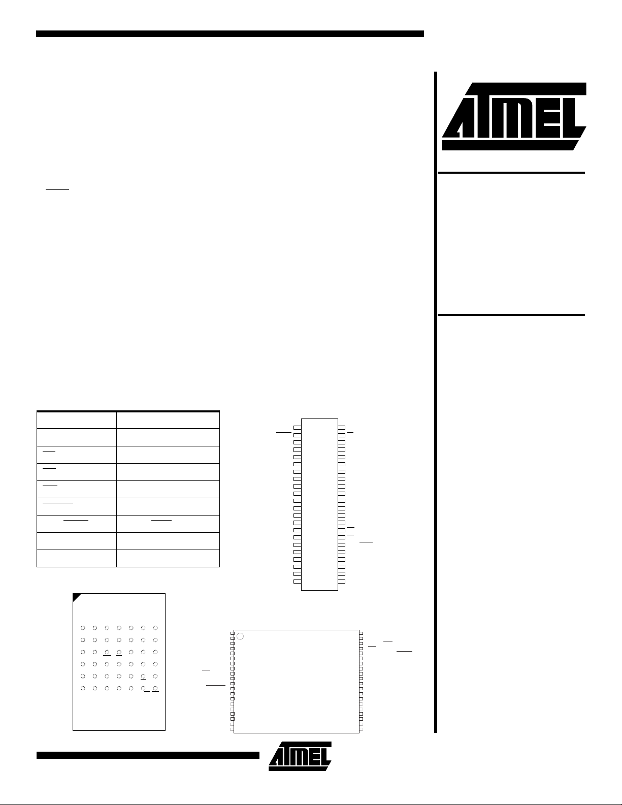
Pin Configurations
Pin Name Function
A0 - A19 Addresses
CE
OE Output Enable
WE
RESET
RDY/BUSY Ready/Busy Outpu t
I/O0 - I/O7 Data Inputs/Outputs
NC No Connect
CBGA Top View
1
Chip Enable
Write Enable
Reset
234567
RESET
A11
A10
I/O0
I/O1
I/O2
I/O3
GND
GND
SOIC
1
NC
A9
A8
A7
A6
A5
A4
NC
NC
A3
A2
A1
A0
44
2
43
3
42
4
41
5
40
6
39
7
38
8
37
9
36
10
35
11
34
12
33
13
32
14
31
15
30
16
29
17
28
18
27
19
26
20
25
21
24
22
23
Flash
Memory
AT49F080
AT49F080T
AT49F080/080T
TSOP Top VIew
A
A5
A8
A11
NC
A12
A15
B
A4
A7
A10
A9
I/O1
A0
I/O0
RST
NC
I/O3
I/O2
VCC
CE
VCC
GND
GND
C
A6
D
A3
E
A2
F
A1
A13
A14
I/O4
I/O6
I/O5
NC
A16
I/O7
OE
RY/BY
A17
A18
A19
NC
NC
WE
A19
A17
A15
A13
CE
NC
A11
A9
A7
A5
A18
A16
A14
A12
VCC
RESET
A10
1
2
3
4
5
6
7
8
9
10
11
12
13
14
15
A8
16
A6
18
19 A2
A4
20
Type 1
NC
OE
I/O7
I/O5
VCC
GND
I/O2
I/O0
A1
A3
NC
WE
RDY/BUSY
I/O6
I/O4
GND
I/O3
I/O1
A0
0584B-A–8/97
40
39
38
37
36
35
34
33
32
31
30
29
28
27
26
25
2417
23
22
21
1
Page 2
To allow for simple in-system reprogrammability, the
AT49F080 does not require high input voltages for programming. 5-volt-only commands determine the read and
programming operat ion of t he de vice . Rea ding data out of
the device is simi lar to r eadin g from an EPROM . Repr ogramming the AT49F080 is performed by erasing the entire
8 megabits of memory and then programming on a byte-bybyte basis. The typical by te progra mming tim e is a fast 10
µs. The end of a p rogr am cy c le ca n be optionally detec ted
by the DATA
polling feature. Once th e end of a byte pro-
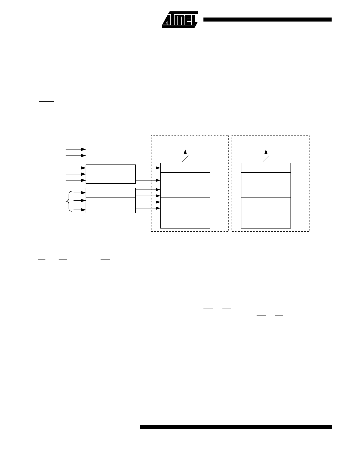
Block Diagram
DATA INPUTS/OUTPUTS
V
CC
GND
OE
WE
CE
ADDRESS
INPUTS
OE, CE, AND WE
LOGIC
Y DECODER
X DECODER
BLOCK (16K BYTES)
gram cycle has be en dete cted, a n ew acce ss for a rea d or
program can begin. The typical number of program and
erase cycles is in excess of 10,000 cycles
The optional 16K bytes boot block section includes a reprogramming write lock out feature to provide data integrity.
The boot sector is designed to contain us er secure code,
and when the featur e is en abled, the b oot se ctor is per manently protected from being reprogrammed.
AT49F080TAT49F080
DATA INPUTS/OUTPUTS
I/O7 - I/O0
8
DATA LATCH
INPUT/OUTPUT
BUFFERS
Y-GATING
FFFFFH FFFFFH
MAIN MEMORY
(1008K BYTES)
03FFFH
OPTIONAL BOOT
00000H
I/O7 - I/O0
8
DATA LATCH
INPUT/OUTPUT
BUFFERS
Y-GATING
OPTIONAL BOOT
BLOCK (16K BYTES)
FC000H
MAIN MEMORY
(1008K BYTES)
00000H
Device Operation
READ:
When CE
at the memory location determined by the add ress pins is
asserted on the outputs. The outputs are put in the high
impedance state whenever CE
line control gives designers flexibility in preventing bus contention.
ERASURE:
1024K bytes memory array ( or 1008K bytes if the boot
block featured is used) must be erased. The erased state
of the memory bits is a logical “1”. The entire device can be
erased at on e time b y using a 6-byt e softw are code . The
software chip erase code consists of 6-byte load commands to specific addr ess location s with a specific data
pattern (please refer to the Chip Erase Cycle Waveforms).
After the software chip eras e has been ini tiated , the devi ce
will internally time the er ase operatio n so that no external
clocks are required. The maximum time needed to era se
the whole chip is t
been enabled, the data in the boot sector will not be
erased.
BYTE PROGRA MMING:
erased, the device is programmed (to a logical “0 ”) on a
The AT49F080 is accessed like an EPROM.
and OE are low and WE is high, the da ta stored
or OE is high. This dual-
Before a byte can be reprogrammed, the
. If the boot block lock out feat ure has
EC
Once the memory array is
byte-by-byte basis. Please note that a data “0” cannot be
programmed ba ck to a “1” ; only er ase op eration s can con vert “0”s to “1”s. Programming is accomplished via the
internal device command register and is a 4 bus cycle operation (please refer to the Com man d De fini ti ons ta ble ). The
device will automatically generate the required internal program pulses.
The program cycle has addresses latched on the falling
edge of WE
latched on the rising edge of WE
first. Programming is completed after the specified t
or CE, whichever occurs last, and the data
or CE, whichever occurs
BP
cycle time. The DATA polling feature may also be use d to
indicate the end of a program cycle.
BOOT BLOCK PROGRAMMING LOCKOUT:
The device
has one designated block that has a programming lockout
feature. This feature prevents programming of data in the
designated block onc e the featu re has been en able d. The
size of the block is 16K bytes. This block, referred to as the
boot block, can contain secure code that is used to bring up
the system. Enabling the lockout feature will allow the boot
code to stay in the device while data in the rest of the
device is update d. This fe ature do es not have to be activated; the boot block 's usage as a write prote ct ed r e gio n i s
2
AT49F080/080T
Page 3

AT49F080/080T
optional to the user. The address range of the AT49F080
boot block is 00000H to 03FFFH while the address range of
the AT49F080T boot block is FC000H to FFFFFH.
To activate the lockout feature, a series of six program
commands to specific addresses with specific data must be
performed. Please refer to the Command Definitions table.
BOOT BLOCK LOCKOUT DETECTION:
method is available to determine if programming of the boot
block section is l ocked out. W hen the device is in the so ftware product iden tification mode (see Soft ware Product
Identification Entry and Exit sections) a read from address
location 00002H will show if program ming the boot bloc k is
locked out. If the data on I/O0 is low, the boot block can be
programmed; if the data on I/O0 is high, the program lockout feature has been activated and the block cannot be
programmed. The s oftwa re p ro duc t identification exit c ode
should be used to return to standard operation.
BOOT BLOCK PROGRAMMING LOCKOUT OVERRIDE:
The user can override the boot block programming
lockout by taking the RESET
this, protected boot block data can be altered through a
chip erase, or byte programming. When the RESET
brought back to TTL levels, the boot block programming
lockout feature is again active.
PRODUCT IDENTIFICATION:
mode identifies the device and manufac turer as Atmel. It
may be accessed by ha rdware or softwar e operatio n. The
hardware operation mode can be used by an external programmer to identify the correct programming algorithm for
the Atmel product.
For details, see Operating Modes (for hardware operation)
or Software Product Identification. The manufacturer and
device code is the same for both modes.
DATA POLLING:
to indicate the end of a program cycle. Dur ing a program
cycle an attempted read of the last byte loaded will result in
the complement of the loa ded data on I/O7. Onc e the program cycle has been com pleted, true data is valid on all
outputs and the next cycle may begin. DATA
begin at any time during the program cycle.
The AT49F080 features DATA
pin to 12V ± 0.5V. By doing
The product identi fication
A software
pin is
polling
polling may
TOGGLE BIT:
provides another method for determining the end of a program or erase cycl e. Du ring a progr am o r er ase opera tion,
successive attempts to read data from the device will result
in I/O6 toggling between one and zero. Once the program
cycle has completed, I/O6 will stop toggling and valid data
will be read. Examining the toggle bit may begin at any time
during a program cycle.
RDY/BUSY
vides another method of detecting the end of a program or
erase operation. RDY/BUSY
the internal program and erase cycles and is released at
the completion of the cycle. The open drain
connection allows fo r OR - tyi ng of sev eral devi ces to the
same RDY/BUSY
RESET:
tem applications. When RESET
device is in its sta nda rd ope ra tin g mo de. A lo w le vel on the
RESET
the outputs of the device in a high impedance state. If the
RESET
or erase operation, the operation may not be successful ly
completed and the op eration wi ll have to be repeated after
a high level is applied to the RESET
is reasserted on the RESET
read or standby mode, depending upon the state of the
control inputs. By applying a 12V ± 0.5V input signal to the
RESET
even if the boot block lockout fea ture has been ena bled
(see Boot Block Programming Lockout Override section).
HARDWARE DATA PROTECTION:
protect against inadvertent programs to the AT49F080 in
the following ways: (a) V
(typical), the program function is inhibited. (b) Program
inhibit: holding any one of OE
inhibits program cycles. (c) Noise filter: pulses of less than
15 ns (typical) on the WE
gram cycle.
input halts the present de vice opera tion and puts
pin makes a high to low transition during a program
pin, the boot block array can be reprogrammed
In addition to DATA
:
An open drain READY/BUSY
line.
A RESET
input pin is provided to ease some sys-
pin, the device returns to the
sense: if VCC is below 3.8V
CC
or CE inputs will not initiate a pro-
polling, the AT49 F080
output pin pro-
is actively pulled low during
is at a l ogic high lev el, t he
pin. When a high level
Hardware features
low, CE high or WE high
3
Page 4
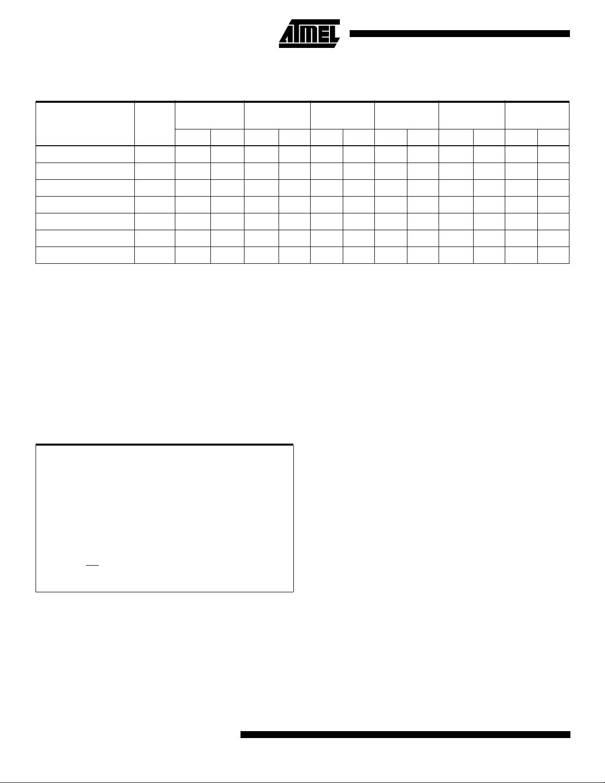
Command Definition (in Hex)
1st Bus
Command
Sequence
Bus
Cycles
Cycle
Addr Data Addr Data Addr Data Addr Data Addr Data Addr Data
2nd Bus
Cycle
3rd Bus
Cycle
4th Bus
Cycle
5th Bus
Cycle
6th Bus
Cycle
Read 1 Addr D
Chip Erase 6 5555 AA 2AAA 55 5555 80 5555 AA 2AAA 55 5555 10
Byte Program 4 555 5 AA 2AAA 55 5555 A0 Addr D
(2)
(2)
(1)
6 5555 AA 2AAA 55 5555 80 5555 AA 2AAA 55 5555 40
3 555 5 AA 2AAA 55 5555 F0
1 XXXX F0
Boot Block Lockout
Product ID Entry 3 5555 AA 2AAA 55 5555 90
Product ID Exit
Product ID Exit
Notes: 1. The 16K byte boot sector has the address range 00000H to 03FFFH for the AT49F080 and FC000H to FFFFFH for the
AT49F080T.
2. Either one of the Product ID Exit commands can be used.
OUT
IN
Absolute Maximum Ratings*
Temperature Under Bias................................ -55°C to +125°C
Storage Temperature..................................... -65°C to +150°C
All Input Voltages
(including NC Pins)
with Respect to Ground...................................-0.6V to +6.25V
All Output Voltages
with Respect to Ground............................-0.6V to V
V oltage on OE
with Respect to Ground...................................-0.6V to +13.5V
4
AT49F080/080T
+ 0.6V
CC
*NOTICE: Stresses beyond those listed under “Absolute
Maximum Ratings” may cause permanent damage to the dev ice . This is a stress rating only an d
functional operati on of the de vi ce at these or an y
other conditions beyond those indicated in the
operational sections of this specification is not
implied. Exposure to absolute maximum rating
conditions f or exten ded periods ma y affect d evice
reliability .
Page 5

AT49F080/080T
DC and AC Operating Range
AT49F080-90 AT49F080-12 AT49F080-15
Operating
Temperature (Case)
V
Power Supply 5V ± 10% 5V ± 10% 5V
CC
Operating Modes
Mode CE OE WE RESET Ai I/O RDY/BUSY
Read V
(2)
Program
Standby/Write
Inhibit
IL
V
IL
V
X
IH
Program Inhibit X X V
Program Inhibit X V
Output Disable X V
RESET XXXV
Product Identification
V
IL
Hardware
Software
(5)
Notes: 1. X can be VIL or VIH.
2. Refer to AC Programming Waveforms.
= 12.0V ± 0.5V
3. V
H
4. Manufacturer Code: 1FH
Device Code: 23H (AT49F080), 27H (AT49F080T)
5. See details under Software Product Identification Entry/Exit..
DC Characteristics
Symbol Parameter Condition Min Max Units
I
LI
I
LO
I
SB1
I
SB2
(1)
I
CC
V
IL
V
IH
V
OL
V
OH1
V
OH2
Note: 1. I
Input Load Current VIN = 0V to V
Output Leakage Current V
VCC Standby Current CMOS CE = V
VCC Standby Current TTL CE = 2.0V to V
V
Active Current f = 5 MHz; I
CC
Input Low Voltage 0.8 V
Input High Voltage 2.0 V
Output Low Voltage IOL = 2.1 mA 0.45 V
Output High Voltage IOH = -400 µA2.4V
Output High Voltage CMOS IOH = -100 µA; VCC = 4.5V 4.2 V
in the erase mode is 90 mA.
CC
Com. 0°C - 70°C 0°C - 70°C 0°C - 70°C
Ind. -40°C - 85°C -40°C - 85°C -40°C - 85°C
V
IL
V
IH
IL
IH
V
IL
V
IH
V
IL
(1)
XV
IH
XV
XV
V
IH
V
IH
V
IH
IH
V
IH
IH
IH
IL
V
IH
A1 - A19 = VIL, A9 = VH,
A1 - A19 = VIL, A9 = VH,
A0 = VIL, A1 - A19 = V
A0 = VIH, A1 - A19 = V
= 0V to V
I/O
Ai D
Ai D
OUT
IN
X High Z V
High Z V
X High Z
CC
CC
A0 = V
A0 = V
(3)
IL
(3)
IH
IL
IL
Manufacturer Code
Device Code
(4)
Manufacturer Code
Device Code
(4)
Com. 100
- 0.3V to V
CC
OUT
CC
CC
Ind. 300
= 0 mA 50 mA
±
10%
V
OH
V
OL
OH
V
OH
V
OH
OH
(4)
(4)
10
10
3mA
µ
A
µ
A
µ
A
µ
A
5
Page 6

AC Read Characteristics
OUTPUT
PIN
5.0V
100 pF
1.8K
1.3K
AT49F080-90 AT49F080-12 AT49F080-15
Symbol Parameter
t
ACC
(1)
t
CE
(2)
t
OE
(3)(4)
t
DF
t
OH
Address to Output Delay 90 120 150 ns
CE to Output Delay 90 120 150 ns
OE to Output De lay 0 40 0 50 0 70 ns
CE or OE to Output Float 0 25 0 30 0 40 ns
Output Hold from OE, CE or Address,
whichever occurre d first
AC Read Waveforms
ADDRESS
CE
OE
OUTPUT
UnitsMinMaxMinMaxMinMax
000ns
ADDRESS VALID
t
CE
t
OE
t
DF
t
ACC
HIGH Z
OUTPUT
VALID
t
OH
Notes: 1. CE may be delayed up to t
2. OE
may be delayed up to tCE - t
change without impact on t
- tCE after the address transition without impact on t
ACC
after the falling edge of CE without impact on tCE or by t
OE
.
ACC
3. tDF is specified from OE or CE whichever occurs first (CL = 5 pF).
4. This parameter is characterized and is not 100% tested
Input Test Waveforms and Measurement level
3.0V
AC
DRIVING
LEVELS
1.5V
AC
MEASUREMENT
LEVEL
0.0V
tR, tF < 5 ns
Pin Capacitance
(f = 1 MHz, T = 25 C)
Typ Max Units Conditions
C
IN
C
OUT
Note: 1. Thi s parameter is characterized and is not 100% tested
6
AT49F080/080T
46 pF V
812 pF V
.
ACC
- tOE after an address
ACC
Output Test Load
= 0V
IN
= 0V
OUT
Page 7

AT49F080/080T
AC Byte Load Characteristics
Symbol Parameter Min Max Units
tAS, t
OES
t
AH
t
CS
t
CH
t
WP
t
DS
tDH, t
OEH
t
WPH
AC Byte Load Waveforms
WE Controlled
Address, OE Set-up Time 0 ns
Address Hold Time 50 ns
Chip Select Set-up Time 0 ns
Chip Select Hold Time 0 ns
Write Pulse Width (WE or CE)90ns
Data Set-up Time 50 ns
Data, OE Hold Time 0 ns
Write Pulse Width High 90 ns
OE
CE
Controlled
ADDRESS
CE
WE
DATA IN
OE
ADDRESS
WE
CE
DATA IN
t
t
t
t
AS
CS
AS
CS
t
OES
t
OES
t
t
AH
AH
t
t
t
DS
t
DS
WP
WP
t
OEH
t
CH
t
WPH
t
DH
t
OEH
t
CH
t
WPH
t
DH
7
Page 8

Program Cycle Characteristics
Symbol Parameter Min Typ Max Units
t
BP
t
AS
t
AH
t
DS
t
DH
t
WP
t
WPH
t
EC
Byte Programming Time 10 50 µs
Address Set-up Time 0 ns
Address Hold Time 50 ns
Data Set-up Time 50 ns
Data Hold Time 0 ns
Write Pulse Width 90 ns
Write Pulse Width High 90 ns
Erase Cycle Time 10 seconds
Program Cycle Waveforms
PROGRAM CYCLE
OE
CE
WE
t
AS
A0-A19
DATA
5555 2AAA 5555
AA 55 A0
Chip Erase Cycle Waveforms
OE
CE
t
WE
t
AS
A0-A19
DATA
5555 2AAA 5555
t
AA 55 80
BYTE 0 BYTE 1 BYTE 2 BYTE 3 BYTE 4 BYTE 5
WP
t
AH
DS
t
WP
t
t
DS
AH
t
WPH
t
DH
t
WPH
t
DH
ADDRESS
INPUT
DATA
5555 2AAA 5555
AA 55 10
t
BP
t
EC
Note: OE must be high only when WE and CE are both low.
8
AT49F080/080T
Page 9

AT49F080/080T
Data Poll ing Characteristics
Symbol Parameter Min Typ Max Units
t
DH
t
OEH
t
OE
t
WR
Data Hold Time 10 ns
OE Hold Time 10 ns
OE to Output Delay
Write Recovery Time 0 ns
(1)
(2)
Notes: 1. These parameters are characterized and not 100% tested
2. See tOE spec in AC Read Characteristics.
Data Polling Waveforms
WE
CE
t
OEH
OE
I/O7
A0-A19
t
DH
t
OE
HIGH Z
An
An An AnAn
t
WR
ns
Toggle Bit Characteristics
Symbol Parameter Min Typ Max Units
t
DH
t
OEH
t
OE
t
OEHP
t
WR
Data Hold Time 10 ns
OE Hold Time 10 ns
OE to Output Delay
OE High Pulse 150 ns
Write Recovery Time 0 ns
(1)
(2)
Notes: 1. These parameters are characterized and not 100% tested.
2. See tOE spec in AC Read Characteristics.
WE
CE
OE
I/O6
(1)(2)(3)
t
OEH
t
DH
t
OEHP
t
OE
HIGH Z
t
WR
Toggle Bit Waveforms
ns
Notes: 1. Toggling either OE or CE or both OE and CE will operate toggle bit. The t
input(s).
2. Beginning and ending state of I/O6 will vary.
3. Any address location may be used but the address should not vary.
specification must be met by the toggling
OEHP
9
Page 10

Software Product
LOAD DATA AA
TO
ADDRESS 5555
LOAD DATA 55
TO
ADDRESS 2AAA
LOAD DATA 80
TO
ADDRESS 5555
LOAD DATA AA
TO
ADDRESS 5555
LOAD DATA 55
TO
ADDRESS 2AAA
LOAD DATA 40
TO
ADDRESS 5555
PAUSE 1 second
(2)
Identification Entry
LOAD DATA AA
ADDRESS 5555
LOAD DATA 55
ADDRESS 2AAA
LOAD DATA 90
ADDRESS 5555
ENTER PRODUCT
IDENTIFICATION
MODE
(1)
TO
TO
TO
(2)(3)(5)
Boot Block Lockout
Feature Enable Algorithm
(1)
Software Product
Identification Exit
LOAD DATA AA
TO
ADDRESS 5555
LOAD DATA 55
TO
ADDRESS 2AAA
LOAD DATA F0
Notes: 1. Data Format: I/O7 - I/O0 (Hex);
TO
ADDRESS 5555
EXIT PRODUCT
IDENTIFICATION
(4)
MODE
2. A1 - A19 = V
3. The device does not remain in identificati on mode if
4. The device returns to standard operation mode.
5. Manufacturers Code: 1FH
Address Format: A14 - A0 (Hex).
Manufacture Code is read for A0 = V
Device Code is read for A0 = V
powered down.
Device Code: 23H (AT49F080), 27H (AT49F080T)
(1)
OR
.
IL
LOAD DATA F0
TO
ANY ADDRESS
EXIT PRODUCT
IDENTIFICATION
.
IH
MODE
;
IL
(4)
Notes: 1. Data Format: I/07 - I/O0 (Hex);
Address Format: A14 - A0 (Hex).
2. Boot block lockout feature enabled.
10
AT49F080/080T
Page 11

Order ing Informat ion
(mA)
I
t
ACC
(ns)
90 50 0.1 AT49F080-90CC
CC
Ordering Code Package Operation RangeActive Standby
AT49F080-90RC
AT49F080-90TC
42C2
44R
40T
AT49F080/080T
Commercial
(0° to 70°C)
50 0.3 AT49F080-90CI
AT49F080-90RI
AT49F080-90TI
120 50 0.1 AT49F080-12CC
AT49F080-12RC
AT49F080-12TC
50 0.3 AT49F080-12CI
AT49F080-12RI
AT49F080-12TI
150 50 0.1 AT49F080-15CC
AT49F080-15RC
AT49F080-15TC
50 0.3 AT49F080-15TI
AT49F080-15TI
AT49F080-15TI
42C2
44R
40T
42C2
44R
40T
42C2
44R
40T
42C2
44R
40T
42C2
44R
40T
Industrial
(-40° to 85°C)
Commercial
(0° to 70°C)
Industrial
(-40° to 85°C)
Commercial
(0° to 70°C)
Industrial
(-40° to 85°C)
(continued)
Pakage Type
42C2 42-Ball, Plastic Chip-Size Ball Grid Array Package (CBGA) 8 x 14 mm
44R 44-Lead, 0.525" Wide, Plastic Gull Wing Small Outline Package (SOIC/SOP)
40T 40-Lead, Thin Small Outline Package (TSOP)
11
Page 12

Order ing Informat ion
(mA)
I
t
ACC
(ns)
90 50 0.1 AT49F080T-90CC
CC
Ordering Code Package Operation RangeActive Standby
AT49F080T-90RC
AT49F080T-90TC
42C2
44R
40T
Commercial
(0° to 70°C)
50 0.3 AT49F080T-90CI
AT49F080T-90RI
AT49F080T-90TI
120 50 0.1 AT49F080T-12CC
AT49F080T-12RC
AT49F080T-12TC
50 0.3 AT49F080T-12CI
AT49F080T-12RI
AT49F080T-12TI
150 50 0.1 AT49F080T-15CC
AT49F080T-15RC
AT49F080T-15TC
50 0.3 AT49F080T-15CI
AT49F080T-15RI
AT49F080T-15TI
42C2
44R
40T
42C2
44R
40T
42C2
44R
40T
42C2
44R
40T
42C2
44R
40T
Industrial
(-40° to 85°C)
Commercial
(0° to 70°C)
Industrial
(-40° to 85°C)
Commercial
(0° to 70°C)
Industrial
(-40° to 85°C)
Pakage Type
42C2 42-Ball, Plastic Chip-Size Ball Grid Array Package (CBGA) 8 x 14 mm
44R 44-Lead, 0.525" Wide, Plastic Gull Wing Small Outline Package (SOIC/SOP)
40T 40-Lead, Thin Small Outline Package (TSOP)
12
AT49F080/080T
 Loading...