

Datasheet AT49F020-55TI, AT49F020-55PI, AT49F020-55PC, AT49F020-55JI, AT49F020-55JC Datasheet (ATMEL)
...Page 1
Features
•
Single Voltage Operation
– 5V Read
– 5V Reprogramming
•
Fast Read Access Time - 55 ns
•
Internal Program Control and Timer
•
8K bytes Boot Block With Lockout
•
Fast Erase Cycle Time - 10 seconds
•
Byte By Byte Programming - 50 µs/Byte
•
Hardware Data Protection
•
DAT A Polling For End Of Program Detection
•
Low Power Dissipation
– 50 mA Active Current
– 100 µA CMOS Standby Current
•
Typical 10,000 Write Cycles
2-Megabit
(256K x 8)
5-volt Only
Description
The AT49F020 is a 5-volt-only in-system Flash Memory. Its 2 megabits of memory is
organized as 262,144 wo rds by 8 bits. M anufac tured with Atmel ’s advanc ed non volatile CMOS technology , the de vice offe rs acc ess t imes to 55 ns with pow er dissip ation
of just 275 mW over the commercial temperature range. When the device is deselected, the CMOS standby current is less than 100
To allow for simple in-system re progr am mab il ity , the AT49F0 20 do es not r equir e hi gh
input voltages for programming. Five-volt-only commands determine the read and
programming operation of the devic e. Reading data out of the device is similar to
reading from an EPROM . Rep ro gramm in g the AT49F020 is performe d by eras i ng t he
entire 2 megabits of memory and then programming on a byte by byte basis. The byte
programming time is a fast 50
detected by the DATA
polling feature. Onc e th e end of a by te p rogr am cyc l e has be en
µs. The end of a program cycle can be optionally
detected, a new access for a read or program can begin. The typical number of program and erase cycles is in excess of 10,000 cycles.
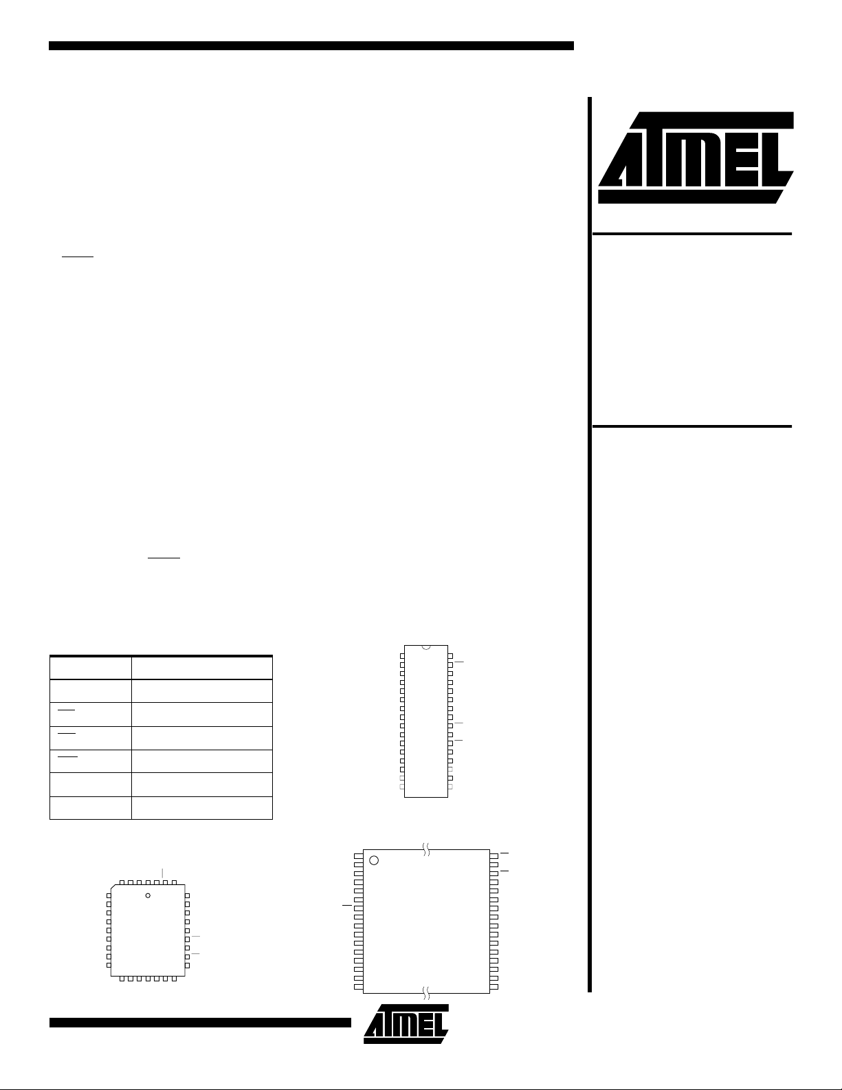
Pin Configurations
Pin Name Function
A0 - A17 Addresses
CE
OE
WE Write Enable
I/O0 - I/O7 Data Inputs/Outputs
Chip Enable
Output En able
µA.
DIP Top View
NC
A16
A15
A12
A7
A6
A5
A4
A3
A2
A1
A0
I/O0
I/O1
I/O2
GND
(continued)
1
32
2
3
4
5
6
7
8
9
10
11
12
13
14
15
16
VCC
31
WE
30
A17
29
A14
28
A13
27
A8
26
A9
25
A11
24
OE
23
A10
22
CE
21
I/O7
20
I/O6
19
I/O5
18
I/O4
17
I/O3
CMOS Flash
Memory
AT49F020
NC No Connect
PLCC Top View
A12
A15
A16NCVCCWEA17
432
1
323130
14151617181920
I/O1
I/O2
I/O3
I/O4
I/O5
GND
29
28
27
26
25
24
23
22
21
I/O6
A14
A13
A8
A9
A11
OE
A10
CE
I/O7
I/O0
5
A7
6
A6
7
A5
8
A4
9
A3
10
A2
11
A1
12
A0
13
VCC
TSOP Top View
Type 1
1
A11
2
A9
3
A8
4
A13
5
A14
6
A17
7
WE
8
9
NC
10
A16
11
A15
12
A12
13
A7
14
A6
15
A5
16
A4
OE
32
A10
31
CE
30
I/O7
29
I/O6
28
I/O5
27
I/O4
26
I/O3
25
GND
24
I/O2
23
I/O1
22
I/O0
21
A0
20
A1
19
A2
18
A3
17
0567B-A–8/97
1
Page 2
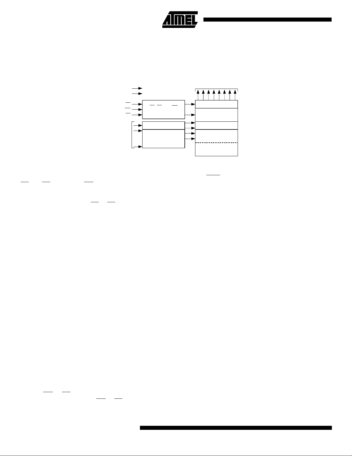
The optional 8K bytes boot block section includes a reprogramming write lock out feature to provide data integrity.
The boot sector is designed to contain us er secure code,
Block Diagram
VCC
GND
and when the featur e is en abled, the b oot se ctor is per manently protected from being reprogrammed.
DATA INPUTS/OUTPUTS
I/O0 - I/O7
OE
WE
CE
ADDRESS
INPUTS
OE, CE AND WE
LOGIC
Y DECODER
X DECODER
Device Operation
READ:
CE
memory location determined by the address pins is
asserted on the outputs . The outputs are p ut in the high
impedance state whenever CE
control gives designers flexibility in preventing bus contention.
ERASURE:
bytes memory array (or 248K bytes if the boot block featured is used) must be erased. The e rased state of the
memory bits is a logical “ 1”. The entire device ca n be
erased at on e time b y using a 6-byt e softw are code . The
software chip erase code consists of 6-byte load commands to specific addr ess location s with a specific data
pattern (please refer to the Chip Erase Cycle Waveforms).
After the software chip eras e has been ini tiated , the devi ce
will internally time the er ase operatio n so that no external
clocks are required. The maximum time needed to erase
the whole chip is t
been enabled, the data in the boot sector will not be
erased.
BYTE PROGRAMMING:
erased, the device is programmed (to a logical “0 ”) on a
byte-by-byte bas is. Please not e that a data “0” ca nnot be
programmed ba ck to a “1”; only er ase oper ation s can co nvert “0”s to “ 1”s. Programmi ng is accompl ished via the
internal device command register and is a 4 bus cycle operation (please r efer to th e Comma nd Defini tions ta ble). The
device will automatically generate the required internal program pulses.
The program cycle has addresses latched on the falling
edge of WE
latched on the rising edge of WE
first. Programming is completed after the specified t
The AT49F020 is ac cessed l ike an EPROM. When
and OE are low and WE is high, the data stored at the
or OE is high. This dual-line
Before a byte can be reprogrammed, the 256K
. If the boot block lockout feature has
EC
Once the memory array is
or CE, whichever occurs last, and the data
or CE, whichever occurs
cycle
BP
DATA LATCH
INPUT/OUTPUT
BUFFERS
Y-GATING
MAIN MEMORY
(248K BYTES)
OPTIONAL BOOT
BLOCK (8K BYTES)
time. The DATA
polling feature may also be used to indicate
the end of a program cycle.
BOOT BLOCK PROGRAMMING LOCKOUT:
The device
has one designated block that has a programming lockout
feature. This feature prevents programming of data in the
designated block once the feature has been enabled. The
size of the block is 8K bytes. This block, referred to as the
boot block, can contain secure code that is used to bring up
the system. Enabling the l ockou t featur e wil l allow t he boot
code to stay in the device while data in the rest of the
device is updated. This feature does not have to be activated; the boot block 's usage as a write pr ote ct ed re gio n i s
optional to the user. The address r ange of the boo t block is
00000H to 01FFFH.
Once the feature is en abled, the data in the boot bl ock c an
no longer be erased or programmed. Data in the main
memory block can still be changed through the regular programming method. To activate the lockout feature, a series
of six program commands to specific addresses wi th specific data must be performed. Please refer to the Command
Definitions table.
BOOT BLOCK LOCKOUT DETECTION:
A software
method is available to determine if programming of the boot
block section is locked out. When the device is in the software product identific ation m ode (see Softwar e Produc t
Identification Entry and Exit sections) a read from address
location 00002H will show if pr ogrammi ng the boot bl ock is
locked out. If the data o n I/O0 is low, the boot bl ock c an be
programmed; if the data on I/O0 is high, the program lockout feature has been activated and the block cannot be
programmed. The software product identification code
should be used to return to standard operation.
2
AT49F020
Page 3
AT49F020
PRODUCT IDENTIFICATION:
The product identification
mode identifies the device and manufacturer as Atmel. It
may be accessed by hardware or software operation. The
hardware operation mode can be used by an external programmer to identify the correct programming algorithm for
the Atmel product.
For details, see Operating Modes (for hardware operation)
or Software Product Identification. The manufacturer and
device code is the same for both modes.
DATA P O L L I N G :
The AT49F020 features DATA
polling to
indicate the end of a program cycle. Dur ing a program
cycle an attempted read of the last byte loaded will result in
the complement of the loaded data on I/O7. Once the program cycle has been com pleted, true data is valid on all
outputs and the next cycle may begin. DATA
polling may
begin at any time during the program cycle.
TOG G L E B I T:
In addition to DATA
polling the AT49F020
provides another method for determining the end of a program or erase cycl e. Du ring a progr am o r er ase opera tion,
successive attempts to read data from the device will result
in I/O6 toggling between one and zero. Once the program
cycle has completed, I/O6 will stop toggling and valid data
will be read. Examining the toggle bit may begin at any time
during a program cycle.
HARDWARE DATA PROTECTION:
Hardware features
protect against inadvertent programs to the AT49F020 in
the following ways: (a) V
sense: i f VCC is below 3 . 8V (t y p-
CC
ical), the program function is inhibited. (b) Program inhibit:
holding any one of OE
low, CE high or WE high inhibits program cycles. (c) Noise filter: pulses of less than 15 ns (typical) on the WE
or CE inputs will not initiate a program
cycle.
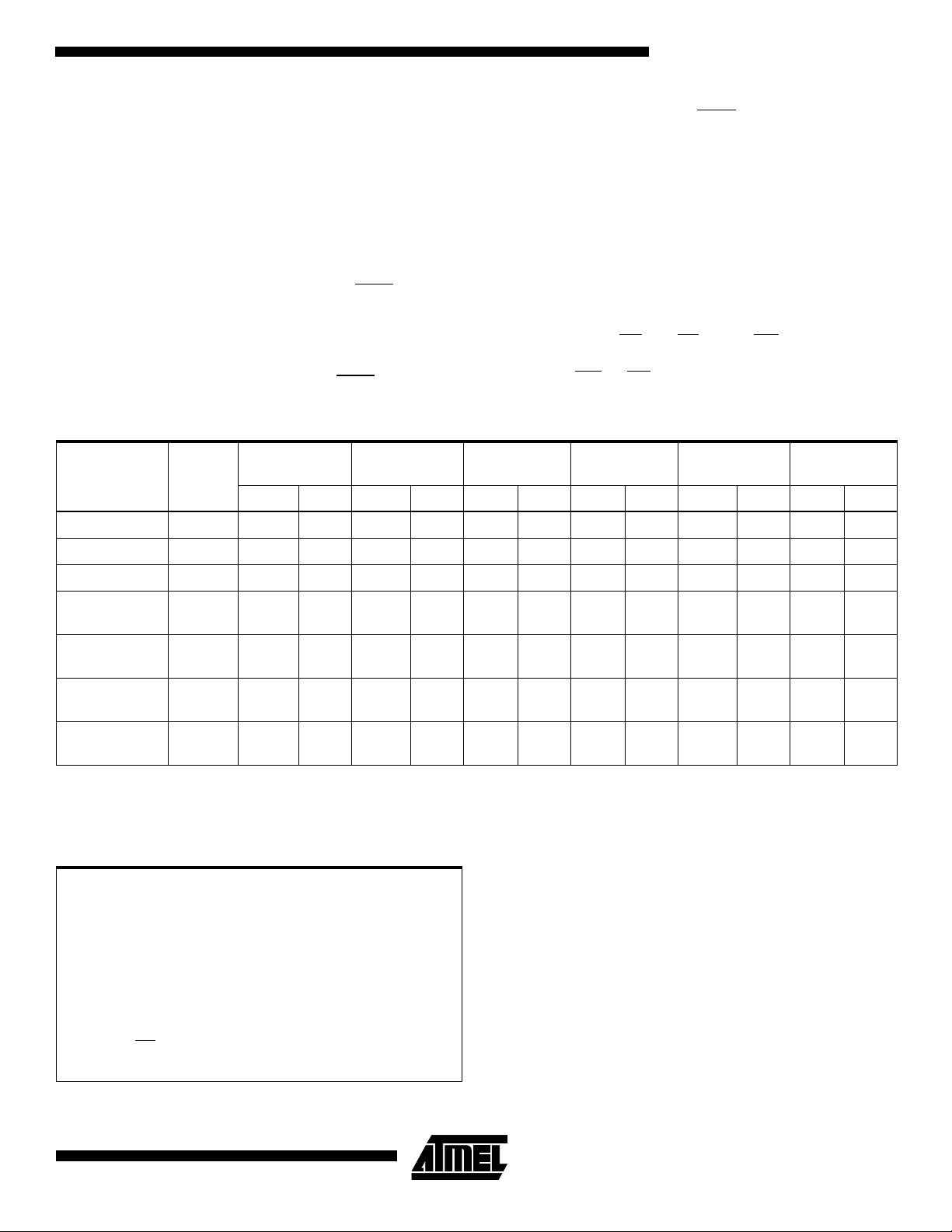
Command Definition (in Hex)
1st Bus
Command
Sequence
Read 1 Addr D
Chip Erase 6 5555 AA 2AAA 55 5555 80 5555 AA 2AAA 55 5555 10
Bus
Cycles
Cycle
Addr Data Addr Data Addr Data Addr Data Addr Data Addr Data
OUT
2nd Bus
Cycle
3rd Bus
Cycle
4th Bus
Cycle
5th Bus
Cycle
6th Bus
Cycle
Byte Program 4 5555 AA 2AAA 55 5555 A0 Addr D
Boot Block
Lockout
Product ID
Entry
Product ID Exit
(2)
Product ID Exit
(2)
Notes: 1. The 8K byte boot sector has the address range 00000H to 01FFFH.
(1)
2. Either one of the Product ID exit commands can be used.
6 5555 AA 2AAA 55 5555 80 5555 AA 2AAA 55 5555 40
3 5555 AA 2AAA 55 5555 90
3 5555 AA 2AAA 55 5555 F0
1 XXXX F0
Absolute Maximum Ratings*
Temperature Under Bias................................ -55°C to +125°C
Storage Temperature..................................... -65°C to +150°C
All Input Voltages (including NC Pins)
with Respect to Ground...................................-0.6V to +6.25V
All Output Voltages
with Respect to Ground.............................-0.6V to V
+ 0.6V
CC
*NOTICE: Stresses beyond those listed under “Absolute
Maximum Ratings” may cause permanent damage to the dev ice . This is a stress rating only an d
functional oper ati on of the device at these or any
other conditions beyond those indicated in the
operational sections of this specification is not
implied. Exposure to absolute maximum rating
conditions f or exten ded periods ma y affect d evice
reliability .
IN
Voltage on OE
with Respect to Ground...................................-0.6V to +13.5V
3
Page 4

DC and AC Operating Range
AT49F020-55 AT49F020-70 AT49F020-90
Operating
Temperature (Case)
Power Supply 5V ± 10% 5V ± 10% 5V ± 10%
V
CC
Com. 0°C - 70°C 0°C - 70°C 0°C - 70°C
Ind. -40°C - 85°C -40°C - 85°C -40°C - 85°C
Operating Modes
Mode CE OE WE Ai I/O
Read V
Program
(2)
Standby/Write Inhibi t V
IL
V
IL
IH
Program Inhibit X X V
Program Inhibit X V
Output Disab le X V
Product Identification
Hardware V
Software
(5)
IL
Notes: 1. X can be VIL or VIH.
2. Refer to AC Programming Waveforms.
3. VH = 12.0V ± 0.5V.
4. Manufacturer Code: 1FH, Device Co de 0BH.
5. See details under Software Product Identification Entry/Exit.
X
V
IL
V
IH
(1)
IL
IH
V
IL
V
IH
V
IL
Ai D
Ai D
XX High Z
IH
X
XHigh Z
A1 - A17 = VIL, A9 = VH,
A0 = V
A0 = V
IL
IH
V
IH
A1 - A17 = VIL, A9 = VH,
A0 = VIL, A1 - A17=V
A0 = VIH, A1 - A17=V
(3)
Manufacturer Code
(3)
Device Code
IL
IL
Manufacturer Code
Device Code
OUT
IN
(4)
(4)
(4)
(4)
DC Characteristics
Symbol Parameter Condition Min Max Units
I
LI
I
LO
I
SB1
I
SB2
(1)
I
CC
V
IL
V
IH
V
OL
V
OH1
V
OH2
Note: In the erase mode, ICC is 90 mA.
4
Input Load Current VIN = 0V to V
Output Leakage Current V
= 0V to V
I/O
CC
CC
10 µA
10 µA
Com. 100 µA
VCC Standby Current CMOS CE = V
VCC Standby Current TTL CE = 2.0V to V
V
Active Current f = 5 MHz; I
CC
- 0.3V to V
CC
OUT
CC
CC
Ind. 300 µA
3mA
= 0 mA 50 mA
Input Low Voltage 0.8 V
Input High Voltage 2.0 V
Output Low Voltage IOL = 2.1 mA .45 V
Output High Voltage IOH = -400 µA2.4V
Output High Voltage CMOS IOH = -100 µA; VCC = 4.5V 4.2 V
AT49F020
Page 5

AT49F020
,
100 pF
1.3K
1.8K
5.0V
OUTPUT
PIN
AC Read Characteristics
AT49F020-55 AT49F020-70 AT49F020-90
Symbol Parameter Min Max Min Max Min Max Units
t
ACC
(1)
t
CE
(2)
t
OE
(3)(4)
t
DF
t
OH
Address to Output Delay 55 70 90 ns
CE to Output Delay 55 70 90 ns
OE to Output Delay 0 30 0 35 0 40 ns
CE or OE to Output Float 025025025ns
Output Hold from OE, CE or
Address, whichever occurred first
000ns
AC Read Waveforms
(1)(2)(3)(4)
ADDRESS
ADDRESS VALID
CE
t
CE
OE
t
DF
.
- tOE after an address change
ACC
OUTPUT
Notes: 1. CE may be delayed up to t
2. OE may be delayed up to tCE - tOE after the falling edge of CE without impact on tCE or by t
without impact on t
ACC
.
t
ACC
HIGH Z
- tCE after the address transition without impact on t
ACC
OUTPUT VALID
t
OH
ACC
3. tDF is specified from OE or CE whichever occurs first (CL = 5 pF).
4. This parameter is characterized and is not 100% tested.
Input Test Waveforms and Measurement Level Output Test Load
AC
DRIVING
LEVELS
t
tF < 5 ns
R
3.0V
0.0V
1.5V
AC
MEASUREMENT
LEVEL
Pin Capacitance
(1)
(f = 1 MHz, T = 25°C)
Typ Max Units Conditions
C
IN
C
OUT
Note: 1. This parameter is characterized and is not 100% tested.
46pFV
812pFV
IN
OUT
= 0V
= 0V
5
Page 6

AC Byte Load Characteristics
Symbol Parameter Min Max Units
tAS, t
OES
t
AH
t
CS
t
CH
t
WP
t
DS
tDH, t
t
WPH
Address, OE Set-up Time 0 ns
Address Hold Time 50 ns
Chip Select Set-up Time 0 ns
Chip Select Hold Time 0 ns
Write Pulse Width (WE or CE)90ns
Data Set-up Time
Data, OE Hold Time 0 ns
OEH
50 ns
Write Pulse Width High 90 ns
AC Byte Load Waveforms
WE Controlled
OE
CE Controlled
ADDRESS
CE
WE
DATA IN
OE
ADDRESS
WE
t
t
t
AS
CS
AS
t
OES
t
OES
t
t
AH
AH
t
t
WP
DS
t
OEH
t
CH
t
WPH
t
DH
t
OEH
t
CH
t
CS
CE
t
t
WP
DS
t
WPH
t
DH
DATA IN
6
AT49F020
Page 7

AT49F020
Program Cycle Characteristics
Symbol Parameter Min Typ Max Units
t
BP
t
AS
t
AH
t
DS
t
DH
t
WP
t
WPH
t
EC
Byte Programming Time 10 50 µs
Address Set-up Time 0 ns
Address Hold Time 50 ns
Data Set-up Time 50 ns
Data Hold Time 0 ns
Write Pulse Width 90 ns
Write Pulse Width High 90 ns
Erase Cycle Time 10 seconds
Program Cycle Waveforms
OE
CE
WE
t
AS
t
WP
t
AH
PROGRAM CYCLE
t
WPH
t
DH
t
BP
A0-A17
DATA
5555 2AAA 5555
AA 55 A0
Chip Erase Cycle Waveforms
OE
CE
t
WP
WE
t
AH
t
DS
AA 55 80
BYTE 0 BYTE 1 BYTE 2 BYTE 3 BYTE 4 BYTE 5
A0-A17
DATA
t
AS
5555 2AAA 5555
t
DS
t
WPH
t
DH
ADDRESS
INPUT
DATA
5555 2AAA 5555
AA 55 10
t
EC
Note: OE must be high only when WE and CE are both low.
7
Page 8

Data Polling Characteristics
(1)
Symbol Parameter Min Typ Max Units
t
DH
t
OEH
t
OE
t
WR
Data Hold Time 10 ns
OE Hold Time 10 ns
OE to Output Delay
(2)
Write Recovery Time 0 ns
Notes: 1. These parameters are characterized and not 100% tested.
2. See tOE spec in AC Read Characteristics
Data Polling Waveforms
WE
CE
t
OEH
OE
I/O7
t
DH
t
OE
t
WR
ns
A0-A17
Toggle Bit Characteristics
(1)
An
An An AnAn
Symbol Parameter Min Typ Max Units
t
DH
t
OEH
t
OE
t
OEHP
t
WR
Data Hold Time 10 ns
OE Hold Time 10 ns
OE to Output Delay
(2)
OE High Pulse 150 ns
Write Recovery Time 0 ns
Notes: 1. These parameters are characterized and not 100% tested.
2. See tOE spec in AC Read Characteristics.
Toggle Bit Waveforms
(1)(2)(3)
WE
CE
OE
I/O6
t
t
DH
OEH
t
OEHP
t
OE
HIGH Z
t
WR
ns
Notes: 1. Toggling either OE or CE or both OE and CE will operate toggle bit. The t
input(s).
2. Beginning and ending state of I/O6 will vary.
3. Any address location may be used but the address should not vary.
8
AT49F020
specification must be met by the toggling
OEHP
Page 9

AT49F020
LOAD DATA AA
TO
ADDRESS 5555
LOAD DATA 55
TO
ADDRESS 2AAA
LOAD DATA 80
TO
ADDRESS 5555
LOAD DATA AA
TO
ADDRESS 5555
LOAD DATA 55
TO
ADDRESS 2AAA
LOAD DATA 40
TO
ADDRESS 5555
PAUSE 1 second
(2)
Software Product
Identification Entry
LOAD DATA AA
ADDRESS 5555
LOAD DATA 55
ADDRESS 2AAA
LOAD DATA 90
ADDRESS 5555
ENTER PRODUCT
IDENTIFICATION
MODE
Software Product
Identification Exit
LOAD DATA AA
TO
ADDRESS 5555
(1)
(1)
TO
TO
TO
OR
(2)(3)(5)
LOAD DATA AA
ANY ADDRESS
TO
Boot Block Lockout Feature
Enable Algorithm
(1)
LOAD DATA 55
TO
ADDRESS 2AAA
LOAD DATA F0
TO
ADDRESS 5555
EXIT PRODUCT
IDENTIFICATION
Notes: 1. Data Format: I/O7 - I/O0 (Hex);
(4)
MODE
2. A1 - A17 = V
3. The device does not remain i n identification mode if
4. The device returns to standard operation mode.
5. Manufacturers Code: 1FH
Address Format: A14 - A0 (Hex).
.
Manufacture Code is read for A0 = V
Device Code is read for A0 = V
powered down.
Device Code: 0BH.
IL
EXIT PRODUCT
IDENTIFICATION
.
IH
MODE
;
IL
(4)
Notes: 1. Data Format: I/O7 - I/O0 (Hex);
Address Format: A14 - A0 (Hex).
2. Boot block lockout feature enabled.
9
Page 10

Order ing Informat ion
I
(mA)
t
ACC
(ns)
55 50 0. 1 AT49F020-55JC 32J Commer cial
70 50 0.1 AT49F020-70JC 32J Commercial
90 50 0.1 AT49F020-90JC 32J Commercial
CC
50 0.3 AT49F020-55JI 32J Industrial
50 0.3 AT49F020-70JI 32J Industrial
50 0.3 AT49F020-90JI 32J Industrial
(1)
Ordering Code Package Operation RangeActive Standby
AT49F020-55PC 32P6 (0° to 70°C)
AT49F020-55TC 32T
AT49F020-55PI 32P6 (-40° to 85°C)
AT49F020-55TI 32T
AT49F020-70PC 32P6 (0° to 70°C)
AT49F020-70TC 32T
AT49F020-70PI 32P6 (-40° to 85°C)
AT49F020-70TI 32T
AT49F020-90PC 32P6 (0° to 70°C)
AT49F020-90TC 32T
AT49F020-90PI 32P6 (-40° to 85°C)
AT49F020-90TI 32T
Note: The AT49F020 has as optional boot block feature. The part number shown in the Ordering Information table is for devices with
the boot block in the lower address range (i.e., 00000H to 01FFFH). Users requiring the boot block to be in the higher address
range should contact Atmel.
Package Type
32J 32 Lead, Plastic, J-Leaded Chip Carrier Package (PLCC)
32P6 32 Lead, 0.600" Wide, Plastic Dual Inline Package (PDIP)
32T 32 Lead, Thin Small Outline Package (TSOP)
10
AT49F020
 Loading...