

Datasheet AT49F008-90TI, AT49F008-90TC, AT49F008-15TI, AT49F008-15TC, AT49F008-12TC Datasheet (ATMEL)
...Page 1
Features
•
Single Voltage Operation
– 5V Read
– 5V Reprogramming
•
Fast Read Access Time - 90 ns
•
Internal Program Control and Timer
•
16K bytes Boot Block With Lockout
•
Fast Erase Cycle Time - 10 seconds
•
Byte-By-Byte Programming - 10 µs/Byte Typical
•
Hardware Data Protection
•
DAT A Polling For End Of Program Detection
•
Low Power Dissipation
– 50 mA Active Current
– 100 µA CMOS Standby Current
•
Typical 10,000 Write Cycles
8-Megabit
(1M x 8)
5-volt Only
Description
The AT49F008 is a 5-volt-o nly in-sys tem Flash Me mory devi ce. Its 8- megabits of
memory is organized as 1,024,576 words by 8-bits. Manufactured with Atmel’s
advanced nonvol atile CMOS technology, the de vi ce of fer s ac ce ss t ime s to 90 ns wi th
power dissipatio n of just 27 5 mW ove r the co mmercia l temper atur e range . When the
device is deselected, the CMOS standby current is less than 100 µA.
(continued)
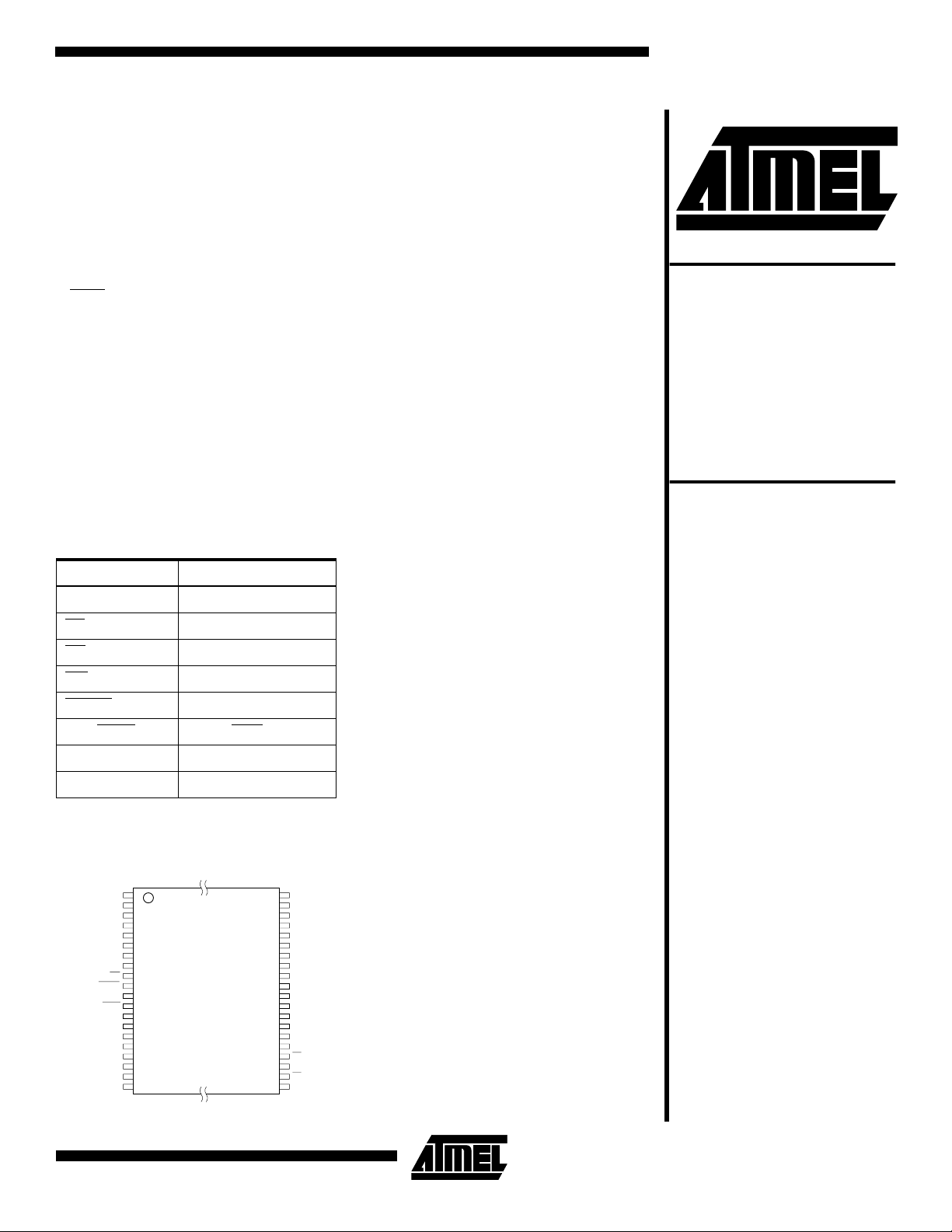
Pin Configurations
Pin Name Function
A0 - A19 Addresses
CE
OE
WE Write Enable
RESET
RDY/BUSY
I/O0 - I/O7 Data Inputs/Outputs
NC No Connect
Chip Enable
Output Enable
Reset
Ready/Busy Output
TSOP Top VIew
Type 1
Flash
Memory
AT49F008
A16
A15
A14
A13
A12
A11
RESET
RDY/BUSY
A18
1
2
3
4
5
6
7
A9
8
A8
9
WE
10
11
NC
12
13
14
A7
15
A6
16
A5
17
A4
18
A3
19
A2
20
A1
40
A17
39
GND
38
NC
37
A19
36
A10
35
I/O7
34
I/O6
33
I/O5
32
I/O4
31
VCC
30
VCC
29
NC
28
I/O3
27
I/O2
26
I/O1
25
I/O0
24
OE
23
GND
22
CE
21
A0
Rev. 0972A–03/98
1
Page 2
To allow for simple in-system reprogrammability, the
AT49F008 does not require high input voltages for programming. 5-volt-only commands determine the read and
programming operation of the device. Reading data out of
the device is similar to reading from an EPROM. Repr ogramming the AT49F008 is performed by erasing the entire
8 megabits of memory and then programming on a byte-bybyte basis. The typical byte programming time is a fast 10
µs. The end of a program cycle can be optionally detected
by the DATA
polling feature. Once the end of a byte pro-
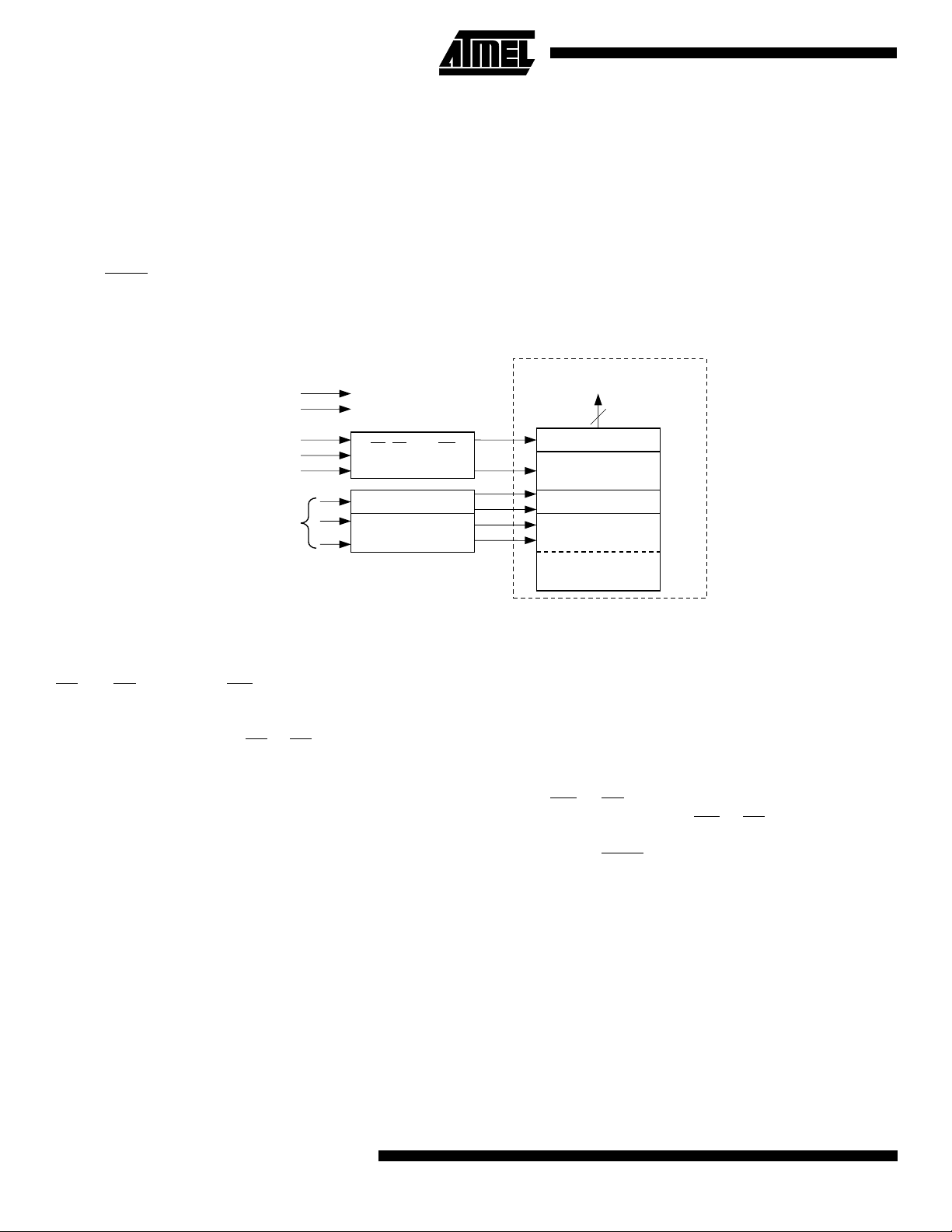
Block Diagram
V
CC
GND
OE
WE
CE
ADDRESS
INPUTS
OE, CE, AND WE
LOGIC
Y DECODER
X DECODER
gram cycle has been detected, a new access for a read or
program can begin. The typical number of program and
erase cycles is in excess of 10,000 cycles
The optional 16K bytes boot block section includes a reprogramming write lock out feature to provide data integrity.
The boot sector is design ed to contai n user secur e code,
and when the featur e is en abled , the b oot s ector i s perma nently protected from being reprogrammed.
DATA INPUTS/OUTPUTS
I/O7 - I/O0
8
DATA LATCH
INPUT/OUTPUT
BUFFERS
Y-GATING
MAIN MEMORY
(1008K BYTES)
OPTIONAL BOOT
BLOCK (16K BYTES)
FFFFFH
03FFFH
00000H
Device Operation
READ:
CE
memory location determined by the address pins is
asserted on the outputs . The outputs ar e put in the high
impedance state whenever CE
control gives designers flexibility in preventing bus contention.
ERASURE:
1024K bytes memo ry array (or 1008K bytes if the boot
block featured is used) must be erased. The erased state
of the memory bits is a logical “1”. The entire device can be
erased at one time by using a 6-byte software code. The
software chi p erase code c onsists of 6-b yte load co mmands to specific address locations with a specific data
pattern (please refer to the Chip Erase Cycle Waveforms).
After the software chip erase has been ini tiated , the devi ce
will internally time the eras e operatio n so that no ex ternal
clocks are required. The maximum time needed to erase
the whole chip is t
been enabled, the data in the boot sector will not be
erased.
BYTE PROGRAMMING:
erased, the device is programmed (to a logical “0”) on a
byte-by-byte bas is. Please note th at a data “0” ca nnot be
The AT49F008 is accessed like an EPROM. When
and OE are low and WE is hi gh, the data st ored at the
or OE is high. This dual-line
Before a byte can be reprogrammed, the
. If the boot block lockout feature has
EC
Once the memory array is
programmed ba ck to a “1”; only era se oper ation s can con vert “0”s to “1 ”s. Programmi ng is accom plished via the
internal device command register and is a 4 bus cycle operation (plea se refer to the Co mmand Defini tions ta ble). The
device will automatically generate the required internal program pulses.
The program cycle has addresses latched on the falling
edge of WE
latched on the rising edge of WE
first. Programming is completed after the specified t
or CE, whichever occurs last, and the data
or CE, whichever occurs
BP
cycle time. The DATA polling feature may also be used to
indicate the end of a program cycle.
BOOT BLOCK PROGRAMMING LOCKOUT:
The device
has one designated block that has a programming lockout
feature. This feature prevents programmin g of data in the
designated block once the feature has been enabled. The
size of the block is 16K bytes. This block, referred to as the
boot block, can contain secure code that is used to bring up
the system. Enablin g the l ocko ut feature will allow t he boot
code to stay in the device while data in the rest of the
device is updated. This feature does not have to be activated; the boot block’ s u sa ge a s a write protected region is
optional to the user. The address range of the AT49F008
boot block is 00000H to 03FFFH.
2
AT49F008
Page 3

AT49F008
To activate the lockout feature, a series of six program
commands to specific addresses with specific data must be
performed. Please refer to the Command Definitions table.
BOOT BLOCK LOCKOUT DETECTION:
method is available to determine if programming of the boot
block section is locked out. When the device is in the software product iden tification mode (see Soft ware Produc t
Identification Entry and Exit sections) a read from address
location 00002H will sho w if progra mming th e boot blo ck is
locked out. If the d ata on I /O 0 i s low, the boo t bl oc k ca n be
programmed; if the data on I/O0 is high, the program lockout feature has been activated and the block cannot be
programmed. The software product identification exit code
should be used to return to standard operation.
BOOT BLOCK PROGRAMMING LOCKO UT OV ERRIDE:
The user can override the boot block programming lockout
by taking the RESET
tected boot block data can be altered through a chip erase,
or byte programming. When the RESET
to TTL levels, the boot block programming lockout feature
is again active.
PRODUCT IDENTIFICATION:
mode identifies the device and manufacturer as Atmel. It
may be accessed by hardware or software operation. The
hardware oper ation mode can be used by an exte rnal programmer to identify the correct programming algorithm for
the Atmel product.
For details, see Operating Modes (for hardware operation)
or Software Product Identification. The manufacturer and
device code is the same for both modes.
DATA POLLING:
indicate the end of a program cycle. During a program
cycle an attempted read of the last byte loaded will result in
the complement of the loaded data on I/O7. Once the program cycle has been com pleted, true data is valid on all
outputs and the next cycle may begin . DATA
begin at any time during the program cycle.
pin to 12V ± 0.5V. By doing this, pr o-
The product identification
The AT49F008 features DATA
A software
pin is brought back
polling to
polling may
TOGGLE BIT:
provides another method for determining the end of a program or erase cycle. During a pro gram or er ase opera tion,
successive attempts to read data from the device will result
in I/O6 toggling between one and zero. Once the program
cycle has completed, I/O6 will stop toggling and valid data
will be read. Examining the toggle bit may begin at any time
during a program cycle.
RDY/BUSY
vides another method of detecting the end of a program or
erase operation. RDY/BUSY
the internal program and erase cycles and is released at
the completion of the cycle. The open drain connection
allows for OR - tying of sever al devices to the same
RDY/BUSY
RESET:
tem applications. When RESET
device is in its sta nda rd ope ra tin g mo de. A lo w level on the
RESET
outputs of the device in a high impedance state, and
reduces the curr ent draw n by the p art to a mi nimum . If the
RESET
or erase operation, the operation may not be successfully
completed and the oper ati on wil l ha ve t o be rep eated afte r
a high level is applied to the RESET
is reasserted on the RESET
read or standby mode, depending upon the state of the
control inputs. By applying a 12V ± 0.5V input signal to the
RESET
even if the boot block lockout feature has been enabled
(see Boot Block Programming Lockout Override section).
HARDWARE DATA PROTECTION:
protect against inadvertent programs to the AT49F008 in
the following ways: (a) V
(typical), the program function is inhibited. (b) Program
inhibit: holding any one of OE
inhibits program cycles. (c) Noise filter: pulses of less than
15 ns (typical) on the WE
gram cycle.
input halts the presen t device opera tion, puts the
pin makes a high to low transition during a program
pin, the boot block array can be reprogrammed
In addition to DATA
:
An open drain READY/BUSY
line.
A RESET
input pin is provided to eas e some sys -
pin, the device returns to the
CC
or CE inputs will not i ni t ia t e a pro-
polling, the AT49F008
output pin pro-
is actively pulled low during
is at a l ogic high le ve l, t he
pin. When a high level
Hardware features
sense: if VCC is below 3.8V
low, CE high or WE high
3
Page 4
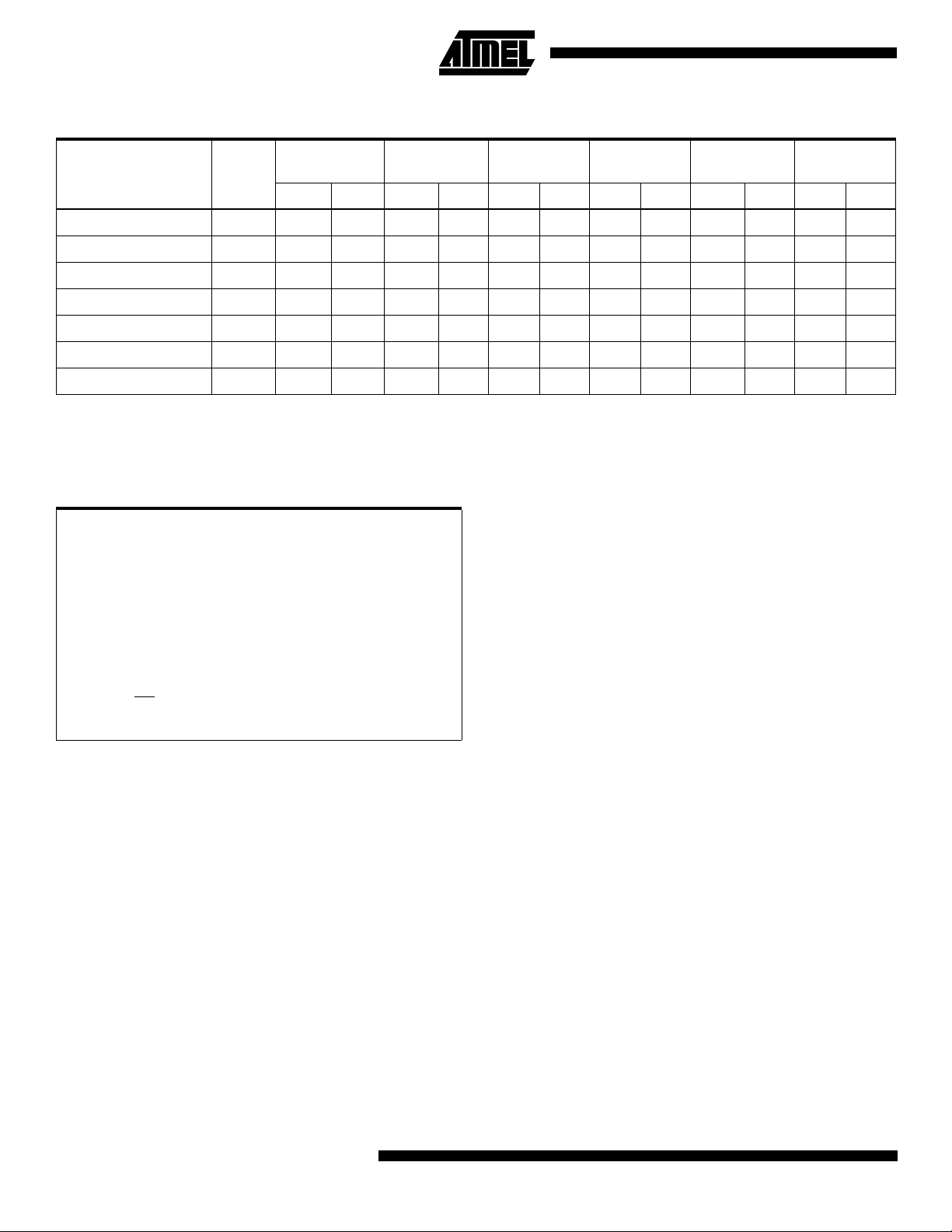
Command Definition (in Hex)
1st Bus
Command
Sequence
Read 1 Addr D
Chip Erase 6 5555 AA 2AAA 55 5555 80 5555 AA 2AAA 55 5555 10
Bus
Cycles
Cycle
Addr Data Addr Data Addr Data Addr Data Addr Data Addr Data
OUT
2nd Bus
Cycle
3rd Bus
Cycle
4th Bus
Cycle
5th Bus
Cycle
6th Bus
Cycle
Byte Program 4 5555 AA 2AAA 55 5555 A0 Addr D
(2)
(2)
(1)
6 5555 AA 2AAA 55 5555 80 5555 AA 2AAA 55 5555 40
3 5555 AA 2AAA 55 5555 F0
1 XXXX F0
Boot Block Lockout
Product ID Entry 3 5555 AA 2AAA 55 5555 90
Product ID Exit
Product ID Exit
Notes: 1. The 16K byte boot sector has the address range 00000H to 03FFFH.
2. Either one of the Product ID Exit commands can be used.
Absolute Maximum Ratings*
Temperature Under Bias................................-55°C to +125°C
Storage Temperature..................................... -65°C to +150°C
All Input Voltages
(including NC Pins)
with Respect to Ground...................................-0.6V to +6.25V
All Output Voltages
with Respect to Ground............................-0.6V to V
Voltage on OE
with Respect to Ground...................................-0.6V to +13.5V
+ 0.6V
CC
*NOTICE: Stresses beyond those listed under “Absolute
Maximum Ratings” may cause permanent damage to the dev ice . This is a s tress rating only an d
functional oper ation of the device at thes e o r any
other conditions beyond those indicated in the
operational sections of this specification is not
implied. Exposure to absolute maximum rating
conditions f or e xtended periods ma y af fect de vice
reliability .
IN
4
AT49F008
Page 5

AT49F008
DC and AC Operating Range
AT49F008-90 AT49F008-12 AT49F008-15
Operating
Temperature (Case)
Power Supply 5V ± 10% 5V ± 10% 5V
V
CC
Operating Modes
Mode CE OE WE RESET Ai I/O RDY/BUSY
Read V
Program
(2)
Standby/Write
Inhibit
IL
V
IL
V
X
IH
Program Inhibit X X V
Program Inhibit X V
Output Disable X V
RESET X X X V
Product Identification
V
IL
Hardware
Software
(5)
Notes: 1. X can be VIL or VIH.
2. Refer to AC Programming Waveforms.
3. VH = 12.0V ± 0.5V
4. Manufacturer C ode: 1FH
Device Code: 22H
5. See details under Software Product Identification Entry/Exit.
DC Characteristics
Symbol Parameter Condition Min Max Units
I
LI
I
LO
I
PD
I
SB1
I
SB2
(1)
I
CC
V
IL
V
IH
V
OL
V
OH1
V
OH2
Note: 1. I
Input Load Current VIN = 0V to V
Output Leakage Current V
Power Down Current RESET = GND ± 0.2V 100
VCC Standby Current CMOS CE = V
VCC Standby Current TTL CE = 2.0V to V
V
Active Current f = 5 MHz; I
CC
Input Low Voltage 0.8 V
Input High Voltage 2.0 V
Output Low Voltage IOL = 2.1 mA 0.45 V
Output High Voltage IOH = -400 µA2.4V
Output High Voltage CMOS IOH = -100 µA; VCC = 4.5V 4.2 V
in the erase mode is 90 mA.
CC
Com. 0°C - 70°C 0°C - 70°C 0°C - 70°C
Ind. -40°C - 85°C -40°C - 85°C -40°C - 85°C
V
IL
V
IH
IL
IH
V
IL
V
IH
V
IL
(1)
XV
IH
XV
XV
V
IH
V
IH
V
IH
IH
V
IH
IH
IH
IL
V
IH
A1 - A19 = VIL, A9 = VH,
A1 - A19 = VIL, A9 = VH,
A0 = VIL, A1 - A19 = V
A0 = VIH, A1 - A19 = V
= 0V to V
I/O
Ai D
Ai D
OUT
IN
X High Z V
High Z V
X High Z
CC
CC
A0 = V
A0 = V
(3)
IL
(3)
IH
IL
IL
Manufacturer Code
Device Code
(4)
Manufacturer Code
Device Code
(4)
Com. 100
- 0.3V to V
CC
OUT
CC
CC
Ind. 300
= 0 mA 50 mA
±
10%
V
OH
V
OL
OH
V
OH
V
OH
OH
(4)
(4)
10
10
3mA
µ
A
µ
A
µ
A
µ
A
µ
A
5
Page 6

AC Read Characteristics
OUTPUT
PIN
5.0V
100 pF
1.8K
1.3K
AT49F008-90 AT49F008-12 AT49F008-15
Symbol Parameter
t
ACC
(1)
t
CE
(2)
t
OE
(3)(4)
t
DF
t
OH
t
RO
Address to Output Delay 90 120 150 ns
CE to Output Delay 90 120 150 ns
OE to Output D elay 0 40 0 50 0 70 ns
CE or OE to Output Float 0 25 0 30 0 40 ns
Output Hold from OE, CE or Address,
whichever occurred first
RESET to Output Delay 800 800 800 ns
AC Read Waveforms
ADDRESS
CE
OE
RESET
OUTPUT
000ns
ADDRESS VALID
t
CE
t
OE
t
ACC
t
RO
HIGH Z
OUTPUT
VALID
UnitsMin Max Min Max Min Max
t
DF
t
OH
Notes: 1. CE may be delayed up to t
2. OE may be delayed up to tCE - t
change without impact on t
- tCE after the address transition without impact on t
ACC
after the falling edge of CE without impact on tCE or by t
OE
.
ACC
3. tDF is specified from OE or CE whichever occurs first (CL = 5 pF).
4. This parameter is characterized and is not 100% tested.
Input Test Waveforms and Measurement level
3.0V
AC
DRIVING
LEVELS
1.5V
0.0V
AC
MEASUREMENT
LEVEL
tR, tF < 5 ns
Pin Capacitance
(f = 1 MHz, T = 25 C)
Typ Max Units Conditions
C
IN
C
OUT
Note: 1. This parameter is characterized and is not 100% tested.
6
46 pF V
812 pF V
AT49F008
.
ACC
- tOE after an address
ACC
Output Test Load
= 0V
IN
= 0V
OUT
Page 7

AT49F008
A C Byte Load Characteristics
Symbol Parameter Min Max Units
t
, t
AS
OES
t
AH
t
CS
t
CH
t
WP
t
DS
t
, t
DH
OEH
t
WPH
AC Byte Load Waveforms
WE Controlled
Address, OE Set-up Time 0 ns
Address Hold Time 50 ns
Chip Select Set-up Time 0 ns
Chip Select Hold Time 0 ns
Write Pulse Width (WE or CE)90ns
Data Set-up Time 50 ns
Data, OE Hold Time 0 ns
Write Pulse Width High 90 ns
OE
CE
Controlled
ADDRESS
CE
WE
DATA IN
OE
ADDRESS
WE
CE
DATA IN
t
t
t
t
AS
CS
AS
CS
t
OES
t
OES
t
t
AH
AH
t
t
t
WP
DS
t
WP
DS
t
OEH
t
CH
t
WPH
t
DH
t
OEH
t
CH
t
WPH
t
DH
7
Page 8

Program Cyc le Characteristics
Symbol Parameter Min Typ Max Units
t
BP
t
AS
t
AH
t
DS
t
DH
t
WP
t
WPH
t
EC
Byte Programming Time 10 50 µs
Address Set-up Time 0 ns
Address Hold Time 50 ns
Data Set-up Time 50 ns
Data Hold Time 0 ns
Write Pulse Width 90 ns
Write Pulse Width High 90 ns
Erase Cycle Time 10 seconds
Program Cycle Waveforms
OE
CE
WE
t
AS
A0-A19
5555 2AAA 5555
t
WP
t
AH
PROGRAM CYCLE
t
WPH
t
DH
ADDRESS
t
BP
t
DS
DATA
AA 55 A0
Chip Erase Cycle Waveforms
OE
CE
t
WP
WE
t
AS
A0-A19
DATA
5555 2AAA 5555
Note: OE must be high only when WE and CE are both low.
t
AH
t
DS
AA 55 80
BYTE 0 BYTE 1 BYTE 2 BYTE 3 BYTE 4 BYTE 5
t
WPH
t
DH
INPUT
DATA
5555 2AAA 5555
AA 55 10
t
EC
8
AT49F008
Page 9

AT49F008
Data Po lling Characteristics
(1)
Symbol Parameter Min Typ Max Units
t
DH
t
OEH
t
OE
t
WR
Data Hold Time 10 ns
OE Hold Time 10 ns
OE to Output Delay
(2)
Write Recovery Time 0 ns
Notes: 1. These parameters are characterized and not 100% tested.
2. See tOE spec in AC Read Characteristics.
Data Polling Waveforms
WE
CE
t
OEH
OE
I/O7
A0-A19
t
DH
t
OE
HIGH Z
An
An An AnAn
t
WR
ns
Toggle Bit Characteristics
(1)
Symbol Parameter Min Typ Max Units
t
DH
t
OEH
t
OE
t
OEHP
t
WR
Data Hold Time 10 ns
OE Hold Time 10 ns
OE to Output Delay
(2)
OE High Pulse 150 ns
Write Recovery Time 0 ns
Notes: 1. These parameters are characterized and not 100% tested.
2. See tOE spec in AC Read Characteristics.
WE
CE
OE
I/O6
(1)(2)(3)
t
OEH
t
DH
t
OEHP
t
OE
HIGH Z
t
WR
Toggle Bit Waveforms
ns
Notes: 1. Toggling either OE or CE or both OE and CE will operate toggle bit. The t
input(s).
2. Beginning and ending state of I/O6 will vary.
3. Any address location may be used but the address should not vary.
specification must be met by the toggling
OEHP
9
Page 10

Software Product
LOAD DATA AA
TO
ADDRESS 5555
LOAD DATA 55
TO
ADDRESS 2AAA
LOAD DATA 80
TO
ADDRESS 5555
LOAD DATA AA
TO
ADDRESS 5555
LOAD DATA 55
TO
ADDRESS 2AAA
LOAD DATA 40
TO
ADDRESS 5555
PAUSE 1 second
(2)
Identification Entry
LOAD DATA AA
ADDRESS 5555
LOAD DATA 55
ADDRESS 2AAA
LOAD DATA 90
ADDRESS 5555
ENTER PRODUCT
IDENTIFICATION
MODE
(1)
TO
TO
TO
(2)(3)(5)
Boot Block Lockout
Feature Enable Algorithm
(1)
Software Product
Identification Exit
LOAD DATA AA
TO
ADDRESS 5555
LOAD DATA 55
TO
ADDRESS 2AAA
LOAD DATA F0
Notes: 1. Data Format: I/O7 - I/O0 (Hex);
TO
ADDRESS 5555
EXIT PRODUCT
IDENTIFICATION
(4)
MODE
2. A1 - A19 = V
3. The device does not remain in identification mode if
4. The device returns to standard operation mode.
5. Manufacturers Code: 1FH
Address Format: A14 - A0 (Hex).
Manufacture Code is read for A0 = V
Device Code is read for A0 = V
powered down.
Device Code: 22H
(1)
OR
.
IL
LOAD DATA F0
TO
ANY ADDRESS
EXIT PRODUCT
IDENTIFICATION
.
IH
MODE
;
IL
(4)
Notes: 1. Data Format: I/07 - I/O0 (Hex);
Address Format: A14 - A0 (Hex).
2. Boot block lockout feature enabled.
10
AT49F008
Page 11

AT49F008
Ordering Information
(mA)
I
t
ACC
(ns)
90 50 0.1 AT49F008-90TC 40T Commercial
120 50 0.1 AT49F008-12TC 40T Commercial
150 50 0.1 AT49F008-15TC 40T Commercial
CC
Ordering Code Package Operation RangeActive Standby
(0° to 70°C)
50 0.3 AT49F008-90TI 40T Industrial
(-40° to 85°C)
(0° to 70°C)
50 0.3 AT49F008-12TI 40T Industrial
(-40° to 85°C)
(0° to 70°C)
50 0.3 AT49F008-15TI 40T Industrial
(-40° to 85°C)
Pakage Type
40T 40-Lead, Thin Small Outline Package (TSOP)
11
Page 12

Packaging Information
, 40-Lead, Plastic Thin Small Outline Package
40T
(TSOP)
Dimensions in Millimeters and (Inches) *
*Controlling dimension: millimeters
© Copyright Atmel Corporation 1998.
Atmel Corporation assumes no responsibility for the use of any circuitry other than circuitry embodied in an
Atmel Corporation product. No other circuit patent licenses are implied. Atmel Corporation’s products are not
authorized for use as critical components in life suppor t devices or systems.
Atmel Headquarters, 2325 Orchard Parkway, San Jose, CA 95131, TEL (408) 441-0311, FAX (408) 487-2600
Atmel Colorado Springs, 1150 E. Cheyenne Mtn. Blvd., Colorado Springs, CO 80906, TEL (719) 576-3300, FAX (719) 540-1759
Atmel Rousset, Zone Industrielle, 13106 Rousset Cedex, France, TEL (33) 4 42 53 60 00, FAX (33) 4 42 53 60 01
Terms and product names in this document may be trademarks of others.
Printed on recycled paper.
0972A–03/98/XM
 Loading...