

Datasheet AT49F002NT-70PC, AT49F002NT-70JI, AT49F002NT-70JC, AT49F002NT-55TI, AT49F002NT-55TC Datasheet (ATMEL)
...Page 1
Features
•
Single Voltage Operation
– 5V Read
– 5V Reprogramming
•
Fast Read Access Time - 55 ns
•
Internal Program Control and Timer
•
Sector Architecture
– One 16K Byte Boot Block with Programming Lockout
– Two 8K Byte Parameter Blocks
– Two Main Memory Blocks (96K, 128K) Bytes
•
Fast Erase Cycle Time - 10 seconds
•
Byte By Byte Programming - 10
•
Hardware Data Protection
•
DAT A Polling For End Of Program Detection
•
Low Power Dissipation
– 50 mA Active Current
µµµµ
– 100
•
Typical 10,000 Write Cycles
A CMOS Standby Current
µµµµ
s/Byte Typical
2-Megabit
(256K x 8)
5-volt Only
CMOS Flash
Description
The AT49F002(N)T is a 5-volt-on ly in- system r eprogramma ble Fl ash Memo ry. Its 2
megabits of memory is organ ized as 262,144 words by 8 bits. Manufactured with
Atmel’s advanced nonvolatile CMOS technology, the device offers access times to 55
ns with power dissipation of just 275 mW over the commercial temperature range.
(continued)
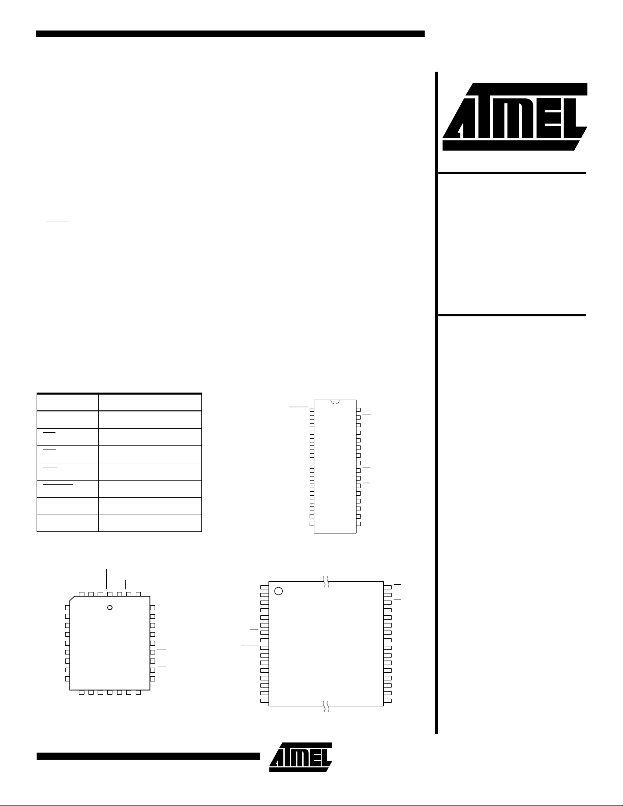
Pin Configurations
Pin Name Function
A0 - A17 Addresses
CE
OE
WE Write Enable
RESET
I/O0 - I/O7 Data Inputs/Outputs
NC No Connect
5
A7
6
A6
7
A5
8
A4
9
A3
10
A2
11
A1
12
A0
13
I/O0
*Note: This pin is a NC on the AT49F002NT.
Chip Enable
Output Enable
RESET
PLCC Top View
A12
A15
A16
RESET *
VCCWEA17
432
1
323130
14151617181920
I/O1
I/O2
I/O3
I/O4
I/O5
GND
29
28
27
26
25
24
23
22
21
I/O6
A14
A13
A8
A9
A11
OE
A10
CE
I/O7
A11
A13
A14
A17
VCC
* RESET
A16
A15
A12
WE
1
2
A9
3
A8
4
5
6
7
8
9
10
11
12
13
A7
14
A6
15
A5
16
A4
DIP Top View
A16
A15
A12
I/O0
I/O1
I/O2
GND
1
2
3
4
5
A7
6
A6
7
A5
8
A4
9
A3
10
A2
11
A1
12
A0
13
14
15
16
* RESET
TSOP Top View
Type 1
32
VCC
31
WE
30
A17
29
A14
28
A13
27
A8
26
A9
25
A11
24
OE
23
A10
22
CE
21
I/O7
20
I/O6
19
I/O5
18
I/O4
17
I/O3
OE
32
A10
31
CE
30
I/O7
29
I/O6
28
I/O5
27
I/O4
26
I/O3
25
GND
24
I/O2
23
I/O1
22
I/O0
21
A0
20
A1
19
A2
18
A3
17
Memory
AT49F002T
AT49F002NT
0920B-B–12/97
1
Page 2
When the device is dese le cted, the CMOS s tandby curren t
is less than 100 µA . For th e AT 49F00 2NT pin 1 for th e DIP
and PLCC packages and pin 9 for the TSOP package are
no connect pins.
To allow for simple in-system reprogrammability, the
AT49F002(N)T does not require high input voltages for programming. Five-vo lt-only comma nds determin e the read
and programming operation of the device. Rea ding data
out of the device is similar to reading from an EPROM; it
has standard CE
, OE, and WE inputs to avoid bus contention. Reprogramming the AT49F002(N)T is performed by
erasing a block of data and then programming on a byte by
byte basis. The byte programming time is a fast 50 µs. The
end of a program cycle can be optionally detected by the
polling feature. Once the end of a byte program
DATA
cycle has been detected, a new access for a read or program can begin. The typ ical numb er of prog ram and era se
cycles is in excess of 10,000 cycles.
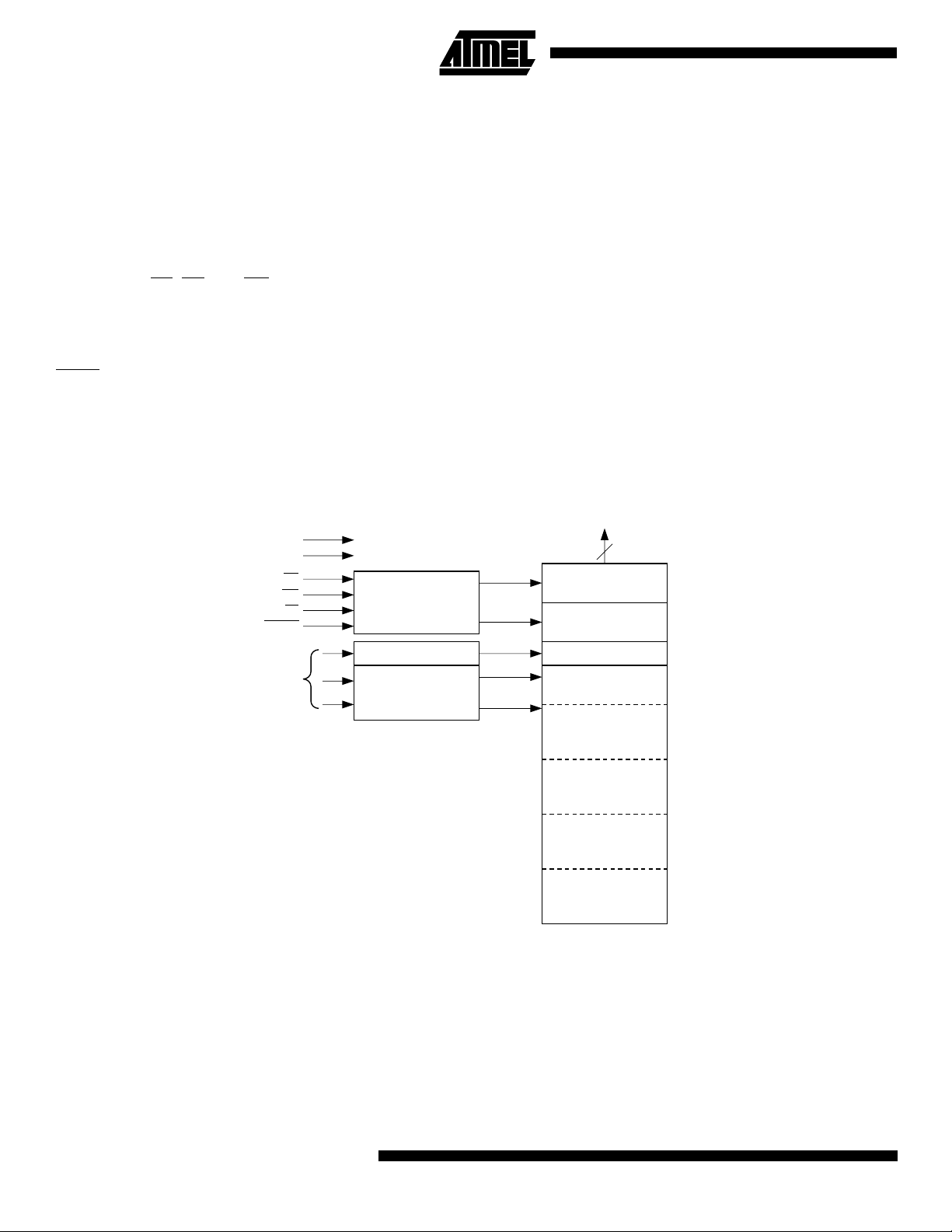
Block Diagram
V
CC
GND
OE
WE
CE
RESET
ADDRESS
INPUTS
CONTROL
LOGIC
Y DECODER
X DECODER
The device is erased by executing the er ase command
sequence; the device internally controls the erase operations. There are two 8K byte parameter block sect ions and
two main memory blocks.
The device has the capability to protect the data in the boot
block; this feature is enabled by a command sequence.
The 16K-byte boot block section includes a reprogramming
lock out feature to pr ovi de data int egrity. The boot sector is
designed to contai n user secu re code, and whe n the feature is enabled, the boot sector is protected from being
reprogrammed.
In the AT49F002NT, once the boot block progr amming
lockout featu re is enabl ed, the co ntents o f the boot bl ock
are permanent and cannot be changed. In the AT49F002T,
once the boot block programming lockout feature is
enabled, the contents of the boot blo ck ca nnot be change d
with input voltage levels of 5.5 volts or less.
DATA INPUTS/OUTPUTS
I/O7 - I/O0
8
INPUT/OUTPUT
BUFFERS
PROGRAM
DATA LATCHES
Y-GATING
BOOT BLOCK
(16K BYTES)
PARAMETER
BLOCK 1
(8K BYTES)
PARAMETER
BLOCK 2
(8K BYTES)
MAIN MEMORY
BLOCK 1
(96K BYTES)
MAIN MEMORY
BLOCK 2
(128K BYTES)
3FFFF
3C000
3BFFF
3A000
39FFF
38000
37FFF
20000
1FFFF
00000
2
AT49F002(N)T
Page 3

Device Operation
READ:
When CE
at the memory location determined by the address pins is
asserted on the outputs . The outputs ar e put in the high
impedance state whenever CE
control gives designers flexibility in preventing bus contention.
COMMAND SEQUENCES:
ered on it will be reset to the read or standby mode
depending upon the state of the control line inputs. In order
to perform other device functions, a series of command
sequences are entered into the device. The command
sequences are shown in the Command Definitions table.
The command sequences are written by applying a low
pulse on the WE
tively) and OE
edge of CE
latched by the first rising ed ge of CE
microprocessor write timings are used. T he address loc ations used in the command sequences are not affected by
entering the command sequences.
RESET:
tem application s. When RESET
device is in its st anda r d ope r atin g mo de. A low level on the
RESET
the outputs of the device in a high impedence state. If the
RESET
or erase operation, the operation may not be sucessfully
completed and the ope ration will have to be repeate d after
a high level is applied to the RESET
is reasserted on the RESET
read or standby mode, depending upon the state of the
control inputs. By appl ying a 12V ± 0.5V inp ut signal to the
RESET
even if the boot block lockout feature has been enabled
(see Boot Block Programming Lockout Override section).
The RESET feature is not available for the AT49F002NT.
0ERASURE:
main memory block or parameter block which contains the
byte must be erased. The erased state of the memory bits
is a logical “1”. The entire device can be erased at one time
by using a 6-byte software code. The software chip erase
code consists of 6-byte load commands to specific address
locations with a specific data pattern (please refer to the
Chip Erase Cycle Waveforms).
After the software chip erase has been ini tiated , the devi ce
will internally time the eras e operatio n so that no ex ternal
clocks are required. The maximum time needed to erase
the whole chip is t
been enabled, the data in the boot sector will not be
erased.
The AT49F002(N)T is access ed like an EPROM .
and OE are low and WE is high, the da ta stor ed
or OE is high. This dual-line
When the device is first pow-
or CE input with CE or WE low ( respec-
high. The addre ss is latche d on the fall ing
or WE, whichever occurs last. The data is
or WE. Standard
A RESET
input halts the present device operation and puts
pin makes a high to low transition during a program
pin, the boot block array can be reprogrammed
input pin is prov ided to ea se som e sys-
is at a logic high le vel, the
pin. When a high level
pin, the device returns to the
Before a byte can be reprogrammed, the
. If the boot block lockout feature has
EC
AT49F002(N)T
CHIP ERASE:
the Chip Erase function will erase Parameter Block 1,
Parameter Block 2, Mai n Memo ry B lock 1, and Main Memory Block 2 but not the boot block. If the Boot Block Lockout
has not been enabled, the Chip Erase function will erase
the entire chip. After the full chip erase the device will
return back to read mode. A ny com man d dur in g ch ip era se
will be ignored.
SECTOR ERASE
device is organized into sectors that can be individually
erased. There are two 8K-byte parameter block sections
and two main memory blocks. The 8K-byte parameter
block sections can be independently erased and reprogrammed. The two main memory sections are designed to
be used as alternative memory sectors. That is, whenever
one of the blocks has been erased and reprogrammed, the
other block should be erased and reprogramm ed before
the first block is again erase d. The Sec tor Eras e command
is a six bus cycle operation. The sector address is latched
on the falling WE
input command is latch ed at the rising edge of WE
sector erase starts after the rising edge of WE
cycle. The erase op eration is in ternally con trolled; it wil l
automatically time to completion.
BYTE PROGRAMMING:
erased, the device is programmed (to a logical “0”) on a
byte-by-byte basi s. Please not e that a data “0” ca nnot be
programmed ba ck to a “1”; only era se oper ation s can con vert “0”s to “1 ”s. Programmi ng is accom plished via the
internal device command register and is a 4 bus cycle operation (plea se refer to the Co mmand Defini tions ta ble). The
device will automatically generate the required internal program pulses.
The program cycle has addresses latched on the falling
edge of WE
latched on the rising edge of WE
first. Programming is completed after the specified t
cycle time. The DATA polling feature may also be used to
indicate the end of a program cycle.
BOOT BLOCK PROGRAMMING LOCKOUT:
has one designated block that has a programming lockout
feature. This feature prevents programmin g of data in the
designated block once the feature has been enabled. The
size of the block is 16K bytes. This block, referred to as the
boot block, can contain secure code that is used to bring up
the system. Enablin g the l ockout fe ature will allow t he boot
code to stay in the device while data in the rest of the
device is updated. This feature does not have to be activated; the boot block’ s u sa ge a s a write protected region is
optional to the user. The address range of the boot block is
3C000 to 3FFFF.
If the boot block lockout has been enabled,
: As an alternative to a full chip erase, the
edge of the sixth cycle while the 30H data
. The
of the sixth
Once the memory array is
or CE, whichever occurs last, and the data
or CE, whichever occurs
BP
The device
3
Page 4

Once the feature is enabled , the data i n the boot b lock can
no longer be erased or programmed. Data in the main
memory block can still be changed through the regular programming method. To activate the lockout feature, a series
of six program commands to specific addresses with specific data must be performed. Please refer to the Command
Definitions table.
BOOT BLOCK LOCKOUT DETECTION:
method is available to determine if programming of the boot
block section is locked out. When the device is in the software product iden tification mode (see Soft ware Produc t
Identification Entry and Exit sections) a read from address
location 00002H will sho w if progra mming th e boot blo ck is
locked out. If the d ata on I /O 0 i s low, the boo t bl oc k ca n be
programmed; if the data on I/O0 is high, the program lockout feature has been activated and the block cannot be
programmed. The software product identification code
should be used to return to standard operation.
BOOT BLOCK PROGRAMMING LOCKOUT OVERRIDE:
The user can override the boot block programming lockout
by taking the RESET
tected boot block data can be altered through a chip erase,
sector erase or word programming. When the RESET
brought back to TTL leve ls the boo t block pr ogramming
lockout feature is again active. This fe ature is not av aila ble
on the AT49F002NT.
PRODUCT IDENTIFICATION:
mode identifies the device and manufacturer as Atmel. It
may be accessed by hardware or software operation. The
hardware oper ation mode can be used by an exte rnal pro-
pin to 12 volts. By doing this, pro-
The product identification
A software
pin is
grammer to identify the correct programm ing algoithm for
the Atmel product.
For details, see Operating Modes (for hardware operation)
or Software Product Identification. The manufacturer and
device code is the same for both modes.
DATA POLLING:
ing to indicate the end of a program cycle. During a program cycle an attempted read of the last byte loaded will
result in the c omple ment of t he load ed data on I/O7 . Once
the program cycle has been completed, true data is valid
on all outputs and the next cycle may begin. DATA
may begin at any time during the program cycle.
TOGGLE BIT:
AT49F002(N)T provides another method for determining
the end of a program or erase cycle. Dur ing a program or
erase operation, successive attempts to read data from the
device will result in I/O6 toggling between one and zero.
Once the program cycle has completed, I/O6 will stop toggling and valid data will be read. Examining the togg le bit
may begin at any time during a program cycle.
HARDWARE DATA PROTECTION:
protect against i nad ve rtent programs to the AT49F002(N)T
in the following ways: (a) V
(typical), the program function is inhibited. (b) Program
inhibit: holding any one of OE
inhibits program cycles. (c) Noise filter: pulses of less than
15 ns (typical) on the WE
gram cycle.
The AT49F002(N)T features DATA
In addition to DATA
sense: if VCC is below 3.8V
CC
low, CE high or WE high
or CE inputs will not i ni t ia t e a pro-
polling the
Hardware features
poll-
polling
4
AT49F002(N)T
Page 5

AT49F002(N)T
Cycle
(1)
OUT
2nd Bus
Cycle
3rd Bus
Cycle
4th Bus
Cycle
5th Bus
Cycle
IN
6th Bus
Cycle
(4)
Command Definition (in Hex)
1st Bus
Command
Sequence
Read 1 Addr D
Chip Erase 6 5555 AA 2AAA 55 5555 80 5555 AA 2AAA 55 5555 10
Sector Erase 6 5555 AA 2AAA 55 5555 80 5555 AA 2AAA 55 SA
Byte Program 4 5555 AA 2AAA 55 5555 A0 Addr D
Boot Block Lockout
Product ID Entry 3 5555 AA 2AAA 55 5555 90
Product ID Exit
Product ID Exit
Notes: 1. The DATA FORMAT in each bus cycle is as follows: I/O7 - I/O0 (Hex)
2. The 16K byte boot sector has the address range 3C000H to 3FFFFH.
3. Either one of the Product ID Exit commands can be used.
4. SA = sector addresses:
(3)
(3)
SA = 3C000 to 3FFFF for BOOT BLOCK
If the boot block is not locked out, this command will erase - BOOT BLOCK, PB1, PB2 and MMB1
If the boot block is locked out, nothing will happen and the device goes back to the read mode in 100 ns
SA = 3A000 to 3BFFF for PARAMETER BLOCK 1
SA = 38000 to 39FFF for PARAMETER BLOCK 2
SA = 20000 to 37FFF for MAIN MEMORY ARRAY BLOCK 1
If the boot block is not locked out, this command will erase - BOOT BLOCK, PB1, PB2 and MMB1
If the boot block is locked out, this command will erase - PB1, PB2 and MMB1
SA = 00000 to IFFFF for MAIN MEMORY ARRAY BLOCK 2
(2)
Bus
Cycles
6 5555 AA 2AAA 55 5555 80 5555 AA 2AAA 55 5555 40
3 5555 AA 2AAA 55 5555 F0
1 XXXX F0
Addr Data Addr Data Addr Data Addr Data Addr Data Addr Data
30
Absolute Maximum Ratings*
Temperature Under Bias................................ -55°C to +125°C
Storage Temperature..................................... -65°C to +150°C
All Input Voltages
(including NC Pins)
with Respect to Ground...................................-0.6V to +6.25V
All Output Voltages
with Respect to Ground............................-0.6V to V
Voltage on OE
with Respect to Ground...................................-0.6V to +13.5V
+ 0.6V
CC
*NOTICE: Stresses beyond those listed under “Absolute Maxi-
mum Ratings” may cause permanent damage to the
device. This is a stress rating only and functional
operation of the device at these or any other c onditions beyond those indicated in the operational sections of this specification is not implied. Exposure to
absolute maximum rating conditions for extended
periods may affect device reliability.
5
Page 6

DC and AC Operating Range
AT49F002(N)T-55 AT49F002(N)T-70
Operating
Temperature (Case)
V
Power Supply 5V ± 10% 5V ± 10%
CC
Com. 0°C - 70°C 0°C - 70°C
Ind. -40°C - 85°C -40°C - 85°C
Operating Modes
Mode CE OE WE RESET
Read V
Program/Erase
(2)
Standby/Write Inhibit V
V
V
IL
V
IL
X
IH
Program Inhibit X X V
Program Inhibit X V
Output Disable X V
V
IL
IH
(1)
IL
IH
IH
V
IL
XV
IH
XV
XV
Reset X X X V
Product Identi fi cation
Hardware
Software
V
(5)
V
IL
V
IL
IH
Notes: 1. X can be VIL or VIH.
2. Refer to AC Programming Waveforms.
= 12.0V ± 0.5V.
3. V
H
4. Manufacturer Code: 1FH, Device Code: 08H
5. See details under Software Product Identification Entry/Exit.
6. This pin is not available on the AT49F002NT.
DC Characteristics
(6)
V
IH
V
IH
IH
V
IH
IH
IH
IL
A1 - A17 = VIL, A9 = VH,
A1 - A17 = VIL, A9 = VH,
A0 = VIL, A1 - A17=V
A0 = VIH, A1 - A17=V
Ai
Ai D
Ai D
X High Z
X High Z
(3)
A0 = V
IL
(3)
A0 = V
IH
IL
IL
I/O
OUT
IN
High Z
Manufacturer Code
Device Code
(4)
Manufacturer Code
Device Code
(4)
(4)
(4)
Symbol Parameter Condition Min Max Units
I
LI
I
LO
Input Load Current VIN = 0V to V
Output Leakage Current V
= 0V to V
I/O
CC
CC
10
10
Com. 100
I
SB1
I
SB2
(1)
I
CC
V
IL
V
IH
V
OL
V
OH1
V
OH2
VCC Standby Current CMOS CE = V
VCC Standby Current TTL CE = 2.0V to V
V
Active Current f = 5 MHz; I
CC
- 0.3V to V
CC
OUT
CC
CC
Ind. 300
= 0 mA 50 mA
3mA
Input Low Voltage 0.8 V
Input High Voltage 2.0 V
Output Low Voltage IOL = 2.1 mA .45 V
Output High Voltage IOH = -400 µA2.4V
Output High Voltage CMOS IOH = -100 µA; VCC = 4.5V 4.2 V
Note: 1. In the erase mode, ICC is 90 mA.
6
AT49F002(N)T
µ
A
µ
A
µ
A
µ
A
Page 7

AC Read Characteristics
t
ACC
t
CE
t
OE
t
DF
t
OH
(1)
(2)
(3)(4)
Address to Output Delay 55 70 ns
CE to Output Delay 55 70 ns
OE to Output Delay 0 30 0 35 ns
CE or OE to Output Float 0 25 0 25 ns
Output Hold from OE, CE or Address,
whichever occurred first
AT49F002(N)T
AT49F002(N)T-55 AT49F002(N)T-70
Min Max Min Max
00 ns
UnitsSymbol Parameter
AC Read Wavef orms
Notes: 1. CE may be delayed up to t
2. OE may be delayed up to tCE - t
change without impact on t
3. t
is specified from OE or CE whichever occurs first (CL = 5 pF).
DF
(1)(2)(3)(4)
ADDRESS
CE
OE
OUTPUT
- tCE after the address transition without impact on t
ACC
OE
.
ACC
ADDRESS VALID
t
CE
t
OE
t
ACC
HIGH Z
after the falling edge of CE without impact on tCE or by t
4. This parameter is characterized and is not 100% tested.
Input Test Waveform and Measurement Level
OUTPUT
VALID
t
DF
t
OH
.
ACC
ACC
Output Loa d Test
- tOE after an address
tR, tF < 5 ns
Pin Capacitance
(f = 1 MHz, T = 25°C)
C
IN
C
OUT
Note: 1. This parameter is characterized and is not 100% tested.
(1)
Typ Max Units Conditions
46 pF V
812 pF V
IN
OUT
= 0V
= 0V
7
Page 8

AC Byte Load Characteristics
Symbol Parameter Min Max Units
tAS, t
OES
t
AH
t
CS
t
CH
t
WP
t
DS
tDH, t
OEH
t
WPH
Address, OE Set-up Time 0 ns
Address Hold Time 50 ns
Chip Select Set-up Time 0 ns
Chip Select Hold Time 0 ns
Write Pulse Width (WE or CE)90ns
Data Set-up Time 50 ns
Data, OE Hold Time
Write Pulse Width High
0ns
90 ns
AC Byte Load Wa veforms
WE Controlled
CE Controlled
OE
ADDRESS
CE
WE
DATA IN
OE
ADDRESS
WE
t
OES
t
t
t
t
AS
CS
OES
AS
t
OEH
t
AH
t
WP
t
DS
t
AH
t
t
OEH
t
CH
CH
t
t
DH
WPH
t
CS
CE
t
WPH
t
WP
t
DS
t
DH
DATA IN
8
AT49F002(N)T
Page 9

AT49F002(N)T
Program Cycle Characteristics
Symbol Parameter Min Typ Max Units
t
BP
t
AS
t
AH
t
DS
t
DH
t
WP
t
WPH
t
EC
Program Cycle Waveforms
Byte Programming Time 10 50 µs
Address Set-up Time 0 ns
Address Hold Time 50 ns
Data Set-up Time 50 ns
Data Hold Time 0 ns
Write Pulse Width 90 ns
Write Pulse Width High 90 ns
Erase Cycle Time 10 seconds
Sector or Chip Erase Cycle Waveforms
(1)
OE
CE
t
WP
WE
AO - A17
DATA
t
AS
t
AH
5555
BYTE 0
t
DH
2AAA 2AAA
t
DS
AA
55 55
BYTE 1 BYTE 2
Notes: 1. OE must be high only when WE and CE are both low.
2. For chip erase, the address should be 5555. For sector erase, the address depends on what sector is to be erased. (See
note 4 under command definitions.)
3. For chip erase, the data should be 10H, and for sector erase, the data should be 30H.
t
WPH
5555
5555
80
AA
BYTE 3
BYTE 4
Note 2
Note 3
BYTE 5
t
EC
9
Page 10

Data Polling Characteristics
(1)
Symbol Parameter Min Typ Max Units
t
DH
t
OEH
t
OE
t
WR
Data Hold Time 10 ns
OE Hold Time 10 ns
OE to Output Delay
(2)
Write Recovery Time 0 ns
Notes: 1. These parameters are characterized and not 100% tested.
2. See t
spec in AC Read Characteristics.
OE
DA T A Polling W aveforms
WE
CE
t
OE
I/O7
t
DH
OEH
t
t
OE
HIGH Z
WR
ns
A0-A17
Toggle Bit Characteristics
(1)
An An An An An
Symbol Parameter Min Typ Max Units
t
DH
t
OEH
t
OE
t
OEHP
t
WR
Data Hold Time 10 ns
OE Hold Time 10 ns
OE to Output Delay
(2)
OE High Pulse 150 ns
Write Recovery Time 0 ns
Notes: 1. These parameters are characterized and not 100% tested.
2. See t
Toggle Bit Waveforms
spec in AC Read Characteristics.
OE
(1)(2)(3)
WE
CE
t
OEH
OE
t
I/O6
DH
t
OEHP
t
OE
HIGH Z
t
WR
ns
Notes: 1. Toggling either OE or CE or both OE and CE will operate toggle bit. The t
input(s).
2. Beginning and ending state of I/O6 will vary.
3. Any address location may be used but the address should not vary.
10
AT49F002(N)T
specification must be met by the toggling
OEHP
Page 11

AT49F002(N)T
LOAD DATA AA
TO
ADDRESS 5555
LOAD DATA 55
TO
ADDRESS 2AAA
LOAD DATA 80
TO
ADDRESS 5555
LOAD DATA AA
TO
ADDRESS 5555
LOAD DATA 55
TO
ADDRESS 2AAA
LOAD DATA 40
TO
ADDRESS 5555
PAUSE 1 second
(2)
Software Product
Identification Entry
LOAD DATA AA
ADDRESS 5555
LOAD DATA 55
ADDRESS 2AAA
LOAD DATA 90
ADDRESS 5555
ENTER PRODUCT
IDENTIFICATION
MODE
Software Product
Identification Exit
LOAD DATA AA
TO
ADDRESS 5555
(1)
(1)
TO
TO
TO
(2)(3)(5)
OR
Boot Block Lockout
Feature Enable Algorithm
Notes for boot block lockout feature enable:
LOAD DATA AA
TO
ADDRESS 5555
1. Data Format: I/O7 - I/O0 (Hex);
Address Format: A14 - A0 (Hex).
2. Boot block lockout feature enabled.
(1)
LOAD DATA 55
TO
ADDRESS 2AAA
LOAD DATA F0
TO
ADDRESS 5555
EXIT PRODUCT
IDENTIFICATION
Notes for software product identification
1. Data Format: I/O7 - I/O0 (Hex);
Address Format: A14 - A0 (Hex).
2. A1 - A17 = V
Manufacture Code is read for A0 = V
Device Code is read for A0 = V
3. The device does not remain in identification mode if
powered down.
4. The device returns to standard operation mode.
MODE
(4)
.
IL
EXIT PRODUCT
IDENTIFICATION
MODE
;
IL
.
IH
(4)
5. Manufacturer Code: 1FH
Device Code: 08H
11
Page 12

Ordering Information
t
ACC
(ns)
55 50 0.1 AT49F002T-55JC
70 50 0.1 AT49F002T-70JC
55 50 0.1 AT49F002NT-55JC
ICC (mA)
Ordering Code Pac kage Operation RangeActive Standby
AT49F002T-55PC
AT49F002T-55TC
50 0.3 AT49F002T-55JI
AT49F002T-55PI
AT49F002T-55TI
AT49F002T-70PC
AT49F002T-70TC
50 0.3 AT49F002T-70JI
AT49F002T-70PI
AT49F002T-70TI
AT49F002NT-55PC
AT49F002NT-55TC
50 0.3 AT49F002NT-55JI
AT49F002NT-55PI
AT49F002NT-55TI
32J
32P6
32T
32J
32P6
32T
32J
32P6
32T
32J
32P6
32T
32J
32P6
32T
32J
32P6
32T
Commercial
(0° to 70°C)
Industrial
(-40° to 85°C)
Commercial
(0° to 70°C)
Industrial
(-40° to 85°C)
Commercial
(0° to 70°C)
Industrial
(-40° to 85°C)
70 50 0.1 AT49F002NT-70JC
AT49F002NT-70PC
AT49F002NT-70TC
50 0.3 AT49F002NT-70JI
AT49F002NT-70PI
AT49F002NT-70TI
Package Type
32J 32-Lead, Plastic, J-Leaded Chip Carrier Package (PLCC)
32J
32P6
32T
32J
32P6
32T
Commercial
(0° to 70°C)
Industrial
(-40° to 85°C)
32P6 32-Lead, 0.600" Wide, Plastic Dual Inline Package (PDIP)
32T 32-Lead, Thin Small Outline Package (TSOP)
12
AT49F002(N)T
 Loading...