

Datasheet AT49BV8192A-20CI, AT49BV8192A-20CC, AT49BV8192A-15TI, AT49BV8192A-15TC, AT49BV8192A-15CI Datasheet (ATMEL)
...Page 1
Features
•
2.7V to 3.6V Read/Write Operation
•
Fast Read Access Time - 120 ns
•
Internal Erase/Program Control
•
Sector Architecture
– One 8K Words (16K bytes) Boot Block with Programming Lockout
– Two 4K Words (8K bytes) Parameter Blocks
– One 496K Words (992K bytes) Main Memory Array Block
•
Fast Sector Erase Time - 10 seconds
•
Byte-by-Byte or Word-By-Word Programming - 30
•
Hardware Data Protection
•
DAT A Polling For End Of Program Detection
•
Low-Power Dissipation
– 25 mA Active Current
µµµµ
–50
A CMOS Standby Current
•
Typical 10,000 Write Cycles
µµµµ
s Typical
8-Megabit
(1M x 8/
512K x 16)
Description
The AT49BV008A(T) and AT49BV8192A(T) are 3-volt, 8-megabit Flash Memories
organized as 1,048,576 words of 8 bits each or 512K words of 16 bits each. Manufactured with Atmel’s advanced nonvolatile CMOS technology, the devices offer access
times to 120 ns with power di ssipati on of jus t 67 mW at 2.7V read . When de selec ted,
the CMOS standby current is less than 50 µA.
The device contains a user-enabled “boot block” protection feature. Two versions of
the feature are available: the AT49BV008A/8192A locates the boot block at lowest
order address es (“bott om boot”); the AT49 BV008AT /8192AT l ocates it at high est
order addresses (“top boot”).
To allow for simple in- system reprog ramma bili ty, the AT49BV 008A(T )/8192A (T) d oes
not require high input voltages for programming. Reading data out of the device is
similar to reading from an EPROM; it has standard CE
bus contention. Reprogramming the AT49BV008A(T)/8192A(T) is performed by first
erasing a block of data and then programming on a byte-by-byte or word-by-word
basis.
, OE, and WE inputs to avoid
(continued)
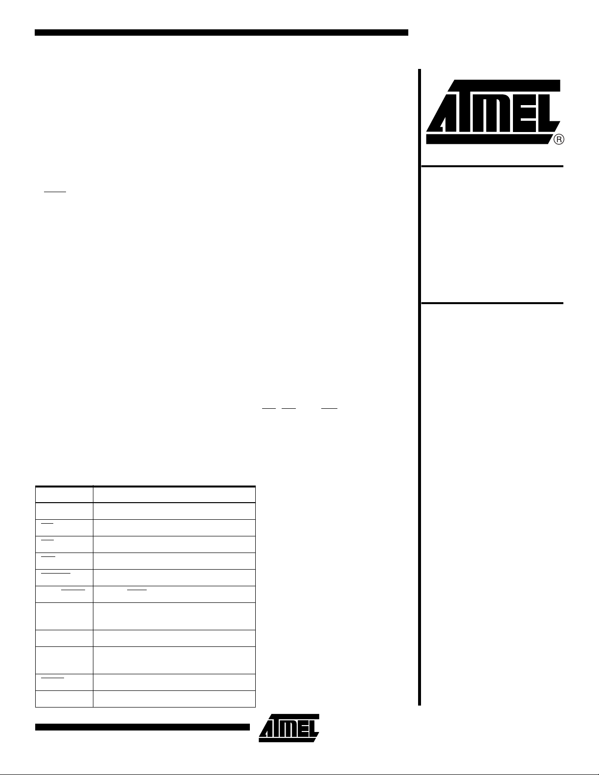
Pin Configurations
Pin Name Function
A0 - A18 Addresses
CE
Chip Enable
CMOS Flash
Memory
AT49BV008A
AT49BV008AT
AT49BV8192A
AT49BV8192AT
Preliminary
OE
WE Write Enable
RESET
RDY/BUSY
VPP
I/O0 - I/O14 Data Inputs/Outputs
I/O15 (A-1)
BYTE Selects Byte or Word Mode
NC No Connect
Output Enable
Reset
Ready/Busy Output
Optional Power Supply for Faster
Program/Era se Op erations
I/O15 (Data Input/Output, Word Mode)
A-1 (LSB Address Input, Byte Mode)
Rev. 1049C–09/98
1
Page 2
AT49BV8192A(T) TSOP Top View
A
B
C
D
E
F
1
234567
A14
A15
A16
A17
NC
GND
A12
A10
A13
NC
A11
I/O7
A8
WE
A9
I/O5
I/O6
NC
VPP
RST
NC
NC
NC
I/O4
NC
A19
NC
I/O2
I/O3
VCC
NC
A18
A6
NC
NC
NC
A7
A5
A3
CE
I/O0
I/O1
8
A4
A2
A1
A0
GND
OE
Type 1
AT49BV008A(T) TSOP Top View
Type 1
1
A15
2
A14
3
A13
4
A12
5
A11
6
A10
7
A9
8
A8
9
NC
10
NC
11
WE
12
RESET
A18
A17
13
14
NC
15
NC
16
17
18
A7
19
A6
20
A5
21
A4
22
A3
23
A2
24
A1
*NC/VPP
AT49BV8192A(T)
CBGA Top View (Ball Down)
234567
1
A
A13
A11
A8
*NC/VPP
B
A14
A10
C
A15
D
A16
E
BYTE
F
GND
A12
I/O14
I/O15
I/O7
WE
I/O5
I/O6
I/O13
NC
RST
A18
A9
NC
NC
I/O11
I/O2
I/O12
I/O3
I/O4
VCC
NC
A17
A6
I/O8
I/O9
I/O10
A7
A5
A3
CE
I/O0
I/O1
8
A4
A2
A1
A0
GND
OE
48
A16
47
BYTE
46
GND
45
I/O15 / A-1
44
I/O7
43
I/O14
42
I/O6
41
I/O13
40
I/O5
39
I/O12
38
I/O4
37
VCC
36
I/O11
35
I/O3
34
I/O10
33
I/O2
32
I/O9
31
I/O1
30
I/O8
29
I/O0
28
OE
27
GND
26
CE
25
A0
RDY/BUSY
AT49BV008A(T) Standard Pin Definition
CBGA Top View (Ball Down)
234567
1
A
A13
A11
A8
VPP
NC
NC
A7
A6
NC
NC
NC
A5
A3
CE
I/O0
I/O1
A4
A2
A1
A0
GND
OE
B
A14
A10
WE
RST
A18
C
A15
A12
D
A16
E
NC
F
GND
NC
A-1
I/O7
A9
I/O5
I/O6
NC
NC
NC
NC
I/O4
A17
NC
I/O2
I/O3
VCC
RESET
*NC/VPP
8
A16
A15
A14
A13
A12
A11
WE
A18
1
2
3
4
5
6
7
A9
8
A8
9
10
11
12
13
14
A7
15
A6
16
A5
17
A4
18
A3
19
A2
20
A1
40
A17
39
GND
38
NC
37
A-1
36
A10
35
I/O7
34
I/O6
33
I/O5
32
I/O4
31
VCC
30
VCC
29
NC
28
I/O3
27
I/O2
26
I/O1
25
I/O0
24
OE
23
GND
22
CE
21
A0
AT49BV008A(T) Alternate Pin Definition
CBGA Top View (Ball Down)
*Standard device is a NC. Please contact Atmel for VPP option.
The device is erased by executing the er ase command
sequence; the device internally controls the erase operation. The memory is divided into four bloc k s for eras e oper ations. There are two 4K word parameter block sections,
the boot block, and the main memor y array blo ck. Th e typ ical number of program and erase cycles is in excess of
10,000 cycles.
The optional 8K word boot block section includes a reprogramming lock out feature to provide data inte grity. This
feature is enabled by a command sequence. Once the boot
block programming lockout feature is enabled, the data in
the boot block cann ot be chan ged when input level s of 3.6
For the AT49BV8192A(T), the BYTE
the device data I/O pi ns op er ate in the by te or wo rd c onfiguration. If the BYTE
pin is set at a logi c “1” o r lef t ope n, the
device is in word co nfigurat ion, I/O0 - I/O15 are activ e and
controlled by CE
If the BYTE
and OE.
pin is set at logic “0”, the devi ce is in byte configuration, and only data I/O pins I/O 0 - I/O7 ar e active an d
controlled by CE
and OE. The data I/O pins I/O8 - I/O14
are tri-stated and the I/O15 pin is used as an input for the
LSB (A-1) address function.
An optional V
pin is available to improve program/erase
PP
times. Please contact Atmel for more information.
pin controls whether
volts or less are used. The boot sector is designed to contain user secure code.
2
AT49BV008A(T)/8192A(T)
Page 3
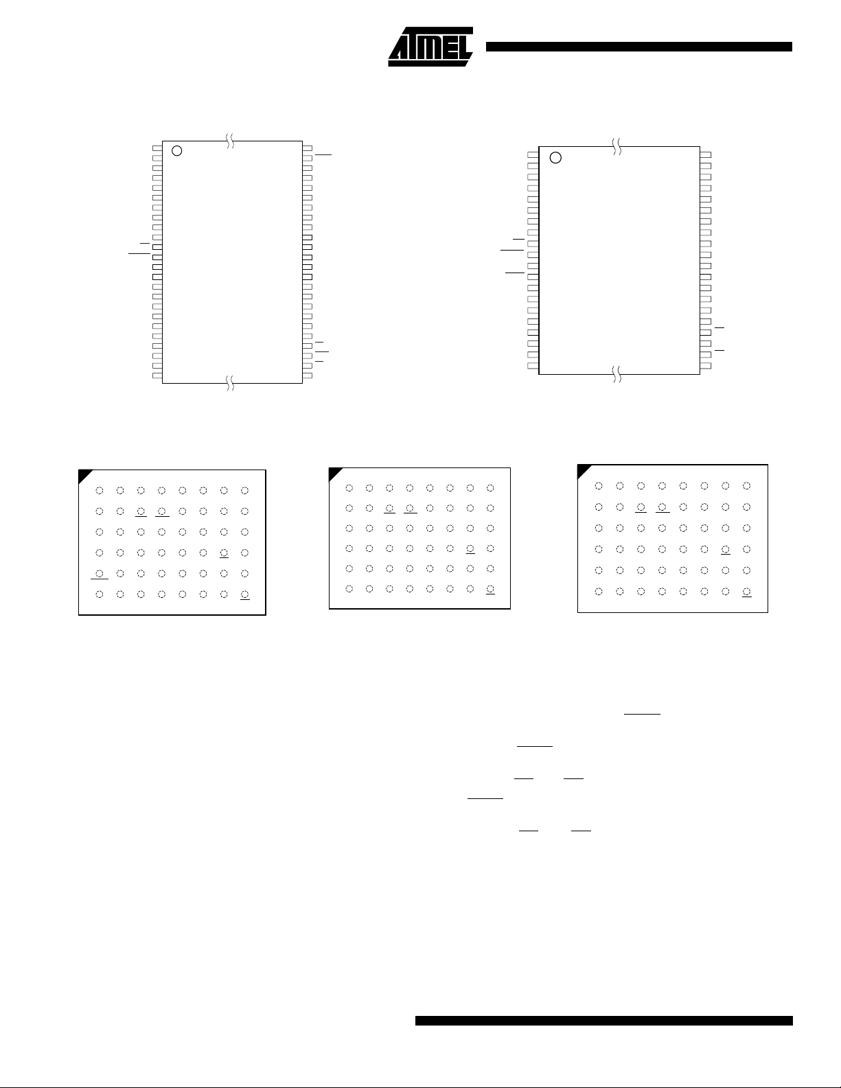
AT49BV008A(T) Block Diagram
V
CC
V
PP
GND
OE
WE
CE
RESET
ADDRESS
INPUTS
CONTROL
LOGIC
Y DECODER
X DECODER
AT49BV8192A(T) Block Diagram
V
CC
V
PP
GND
AT49BV008A AT49BV008AT
DATA INPUTS/OUTPUTS
I/O0 - I/O7
INPUT/OUTPUT
BUFFERS
PROGRAM DATA
LATCHES
Y-GATING
MAIN MEMORY
(992K BYTES)
PARAMETER
BLOCK 2
8K BYTES
PARAMETER
BLOCK 1
8K BYTES
BOOT BLOCK
16K BYTES
AT49BV8192A AT49BV8192AT
DATA INPUTS/OUTPUTS
I/O0 - I/O15
AT49BV008A(T)/8192A(T)
DATA INPUTS/OUTPUTS
I/O0 - I/O7
INPUT/OUTPUT
BUFFERS
PROGRAM DATA
LATCHES
FFFFF FFFFF
08000
07FFF
06000
05FFF
04000
03FFF
00000 00000
DATA INPUTS/OUTPUTS
Y-GATING
BOOT BLOCK
16K BYTES
PARAMETER
BLOCK 1
8K BYTES
PARAMETER
BLOCK 2
8K BYTES
MAIN MEMORY
(992K BYTES)
I/O0 - I/O15
FC000
FBFFF
7A000
79FFF
78000
77FFF
OE
WE
CE
RESET
ADDRESS
INPUTS
CONTROL
LOGIC
Y DECODER
X DECODER
INPUT/OUTPUT
BUFFERS
PROGRAM DATA
LATCHES
Y-GATING
MAIN MEMORY
(496K WORDS)
PARAMETER
BLOCK 2
4K WORDS
PARAMETER
BLOCK 1
4K WORDS
BOOT BLOCK
8K WORDS
Device Operation
READ:
EPROM. When CE
data stored at the memory location determined by the
address pins is asserted on the outputs. The outputs are
put in the high impedance state whenever CE
high. This dual-line con tr ol gi v es d esign er s fl ex ibi lit y in pr eventing bus contention.
COMMAND SEQUENCES:
ered on it will be reset to the read or standby mode
depending upon the state of the control line inputs. In order
to perform other device functions, a series of command
sequences are entered into the device. The command
The AT49BV008A(T)/8192A(T) is accessed like an
and OE are low and WE is high, th e
or OE is
When the device is first pow-
INPUT/OUTPUT
BUFFERS
PROGRAM DATA
LATCHES
7FFFF 7FFFF
04000
03FFF
03000
02FFF
02000
01FFF
00000 00000
Y-GATING
BOOT BLOCK
8K WORDS
PARAMETER
BLOCK 1
4K WORDS
PARAMETER
BLOCK 2
4K WORDS
MAIN MEMORY
(496K WORDS)
7E000
7DFFF
7D000
7CFFF
7C000
7BFFF
sequences are shown in the Com mand Definition s table
(I/O8 - I/O15 are don't care inputs for the command codes).
The command sequences are written by applying a low
pulse on the WE
tively) and OE
edge of CE
latched by the first rising edge of CE
or CE input with CE or WE low (respec-
high. The address is latched on the falling
or WE, whichever occurs last. The data is
or WE. Standard
microprocessor write timings are used. The address locations used in the command sequences are not affected by
entering the command sequences.
RESET:
A RESET
tem applications. When RESET
input pin is prov ided to eas e so me s ys-
is at a logic high level, the
3
Page 4

device is in its standa rd oper at ing mod e. A low l ev el on the
RESET
the outputs of the de vice in a hi gh imped ance stat e. When
a high level is reasse rted on the RES ET
returns to the Read or Standby mod e, depending upon the
state of the control inputs. By applying a 12V ± 0.5V input
signal to the RE SE T
grammed even if the boot block program lockout feature
has been enable d (see Boot B lock Pr ogrammi ng Lock out
Override section).
ERASURE:
must be erased. The erased state of memory bits is a logical “1”. The entire device can be erased by using the Chip
Erase command or individual sectors can be erased by
using the Sector Erase commands.
CHIP ERASE:
by using the 6-byte chip erase software code. After the chip
erase has been initiated, the device will internally time the
erase operation so that no external clocks are required.
The maximum time to erase the chip is t
If the boot block lockou t has be en enabled, the Ch ip Eras e
will not erase the data in t he boot block; it wil l erase the
main memory block and the parameter blocks only. After
the chip erase, the de vi ce wi ll retu rn to the read or standby
mode.
SECTOR ERASE:
device is organized into four sectors that can be individually
erased. There are two 4K word parameter block sections,
one boot block, and the main memory array block. The
Sector Erase command is a six bus cycle operation. The
sector address is latched on the falling WE
sixth cycle while the 30 H data in put com mand is la tched at
the rising edge of WE
ing edge of WE
internally controlled; it will automatically time to completion.
Whenever the main memory block is erased and reprogrammed, the two parame ter bloc ks should be erased and
reprogrammed before the main memory block is erased
again. Whenever a parameter block is erased and reprogrammed, the other parameter block should be erased and
reprogrammed before the first parameter block is erased
again.
BYTE/WORD PROGRAMMING:
erased, it is programmed (to a logical “0”) on a byte-by-byte
or word-by-word bas is. Progr amming is accom plished via
the internal device command register and is a 4 bus cycle
operation. The device will automatically generate the
required internal program pulses.
Any commands written to the c hip during the em bedded
programming cycle will be ignored. If a hardware reset happens during programming, the data at the location being
programmed will be corrupted. Please note that a data “0”
input halts the prese nt device oper ation and puts
pin, the device
pin the boot blo ck ar ray c an b e r epro-
Before a byte or word can be reprogrammed, it
The entire device can be erased at one time
.
EC
As an alternative to a full chip erase, the
edge of the
. The sector erase s tar ts after the ris-
of the sixth cycle. The erase o peration is
Once a memory block is
cannot be programmed back to a “1”; only erase operations
can convert “ 0”s to “ 1”s. Pro grammi ng is co mplete d after
the specified t
also be used to indicate the end of a program cycle.
BOOT BLOCK PROGRAMMING LOCKOUT:
has one designated block that has a programming lockout
feature. This feature prevents programming of data in th e
designated block once the feature has been enabled. The
size of the block is 8K words. Thi s blo ck, refe rred to a s the
boot block, can contain secure code that is used to bring up
the system. Enablin g the l ockou t feature w ill al low the boot
code to stay in the device while data in the rest of the
device is updated. This feature does not have to be activated; the boot block’ s u sag e as a wr i te pro t ected r eg io n is
optional to the user. The address range of the boot block is
00000H to 03FFFH for the AT49BV008A; FC000H to
FFFFFH for the AT49BV008AT; 00000H to 01FFFH for the
AT49BV8192A; and 7E000H to 7FFFFH for the
AT49BV8192AT.
Once the feature is enabled, the data in the boot blo ck ca n
no longer be erased or programmed when input levels of
5.5V or less are u sed. Dat a in the ma in memo ry bloc k can
still be changed through the regular programming method.
To activate the lockout feature, a series of six program
commands to specific addresses with specific data must be
performed. Please refer to the Command Definitions table.
BOOT BLOCK LOCKOUT DETECTION:
method is available to determine if programming of the boot
block section is locked out. When the device is in the software product identification mode (see Software Product
Identification Entry and Exit section s) a read from the following address location will show if programming the boot
block is lock ed out—00002H for the AT4 9BV008A an d
AT49BV8192A; FC002H for the AT49BV008AT; and
7E002H for the AT49B V8192AT. If the da ta on I/O0 is low,
the boot block can be programmed; if the data on I/O0 is
high, the program lockout feature has been enabled and
the block cann ot be programm ed. The soft ware product
identification exit code should be used to return to standard
operation.
BOOT BLOCK PROGRAMMING LOCKOUT OVERRIDE:
The user can override th e boot blo ck progr amming lo ckout
by taking the RESET
erase, sector erase or word pro grammin g oper ation. W hen
the RESET
programming lockout feature is again active.
PRODUCT IDENTIFICATION:
mode identifies the device and manufacturer as Atmel. It
may be accessed by hardware or software operation. The
hardware operation mode can be used by an external programmer to identify the correct programming algorithm for
the Atmel product.
cycle time. The DATA polling feature may
BP
The device
A software
pin to 12 volts during the entire chip
pin is brought back to TTL levels the boot block
The product identification
4
AT49BV008A(T)/8192A(T)
Page 5

AT49BV008A(T)/8192A(T)
For details, see O peratin g Modes (for har dware operatio n)
or Software Product Identification. The manufacturer and
device code is the same for both modes.
DATA POLLING:
polling to indic ate the en d o f a program cycle. Dur in g
DATA
The AT49BV008A(T)/8192A(T) features
a program cycle an attempted read of the last byte loaded
will result in the complement of the loaded data on I/O7.
Once the program cycle has been completed, true data is
valid on all outputs and th e next cyc le may be gin. Du ring a
chip or sector erase operation, an attempt to read the
device will give a “0” on I/O7. Once the program or erase
cycle has completed, true data will be read from the device.
polling may begi n at any ti me during the program
DATA
cycle.
TOGGLE BIT:
In addition to DATA
polling the
AT49BV008A(T)/8192A(T) provides another method for
determining the end of a program or erase cycle. During a
program or erase operation, successive attempts to read
data from the de vice will res ult in I/O6 toggling be tween
one and zero. Once the program cycle has completed, I/O6
will stop toggling and valid data will be read. Examining the
toggle bit may begin at any time during a program cycle.
READY/BUSY
drain READY/BUSY
:
For the AT49F008A(T), pin 12 i s an open
output pin whic h provides a nother
method of detecting the end of a program or erase operation. RDY/BUSY
is activ ely pu lled lo w dur ing th e inte rnal
program and erase cycles and it is rele ased at the co mpletion of the cycle. The open drain connec tion allow s for ORtying of several devices to the same RDY/BUSY
HARDWARE DATA PROTECTION:
Hardware features
line.
protect against inadvertent programs to the
AT49BV008A(T)/8192A(T) in the following ways: (a) V
CC
sense: if VCC is below 1.8V (typical), the program function
is inhibited. (b) V
the V
sense level, the device will automaticall y time out
CC
power on delay: onc e VCC has reached
CC
10 ms (typical) before programming. (c) Program inhibit:
holding any one of OE
low, CE high or WE h igh inhi bits
program cycles. (d) Noise filter: pulses o f less than 15 ns
(typical) on the WE
or CE inputs will not initiate a program
cycle.
INPUT LEVELS:
While operating with a 2.7V to 3.6V
power supply, th e address inpu ts and cont rol inputs (OE
, and WE) may be dr iven from 0 to 5.5V without
CE
adversely affecting the operation of the device. The I/O
lines can only be driven from 0 to V
AT49BV008A(T) ALTERNATE PIN DEFINITION:
+ 0.6V.
CC
Two
AT49BV008A(T) BGA pin definitions are shown. The standard pin definition allows use of the JEDEC standard programming algorithm. If the alternate pin definition is used,
the programming algorithm must be modified as shown in
the Command Definition for Alternate Pin Definition Table
on page 7.
,
5
Page 6

Command Definition in (in Hex)
1st Bus
Command
Sequence
Read 1 Addr D
Chip Erase 6 5555 AA 2AAA 55 5555 80 5555 AA 2AAA 55 5555 10
Sector Erase 6 5555 AA 2AAA 55 5555 80 5555 AA 2AAA 55 SA
Byte/Word Program 4 5555 AA 2AAA 55 5555 A0 Addr D
Boot Block Lockout
Product ID Entry 3 5555 AA 2AAA 55 5555 90
Product ID Exit
Product ID Exit
Notes: 1. The DATA FORMAT in each bus cycle is as follows: I/O15 - I/O8 (Don’t Care); I/O7 - I/O0 (Hex)
(3)
(3)
The ADDRESS FORMAT in each bus cycle is as follows: A15 - A0 (Hex), A-1, and A15 - A18 (Don’t Care)
2. The boot sector has the address range
Bus
Cycles
(2)
6 5555 AA 2AAA 55 5555 80 5555 AA 2AAA 55 5555 40
3 5555 AA 2AAA 55 5555 F0
1xxxxF0
Cycle
Addr Data Addr Data Addr Data Addr Data Addr Data Addr Data
OUT
2nd Bus
Cycle
3rd Bus
Cycle
4th Bus
Cycle
5th Bus
Cycle
IN
6th Bus
Cycle
(4)
00000H to 03FFFH for the AT49BV008A; FC000H to FFFFFH for the
AT49BV008AT; 00000H to 01FFFH for the AT49BV8192A; and 7E000H to 7FFFFH for the AT49BV8192AT
3. Either one of the Product ID Exit commands can be used.
4. SA = sector addresses: (A0 - A18)
For the AT49BV008A/8192A
SA = 01XXX for BOOT BLOCK
SA = 02XXX for PARAMETER BLOCK 1
SA = 03XXX for PARAMETER BLOCK 2
SA = 7FXXX for MAIN MEMORY ARRAY
30
.
For the AT49BV008AT/8192AT
SA = 7FXXX for BOOT BLOCK
SA = 7DXXX for PARAMETER BLOCK 1
SA = 7CXXX for PARAMETER BLOCK 2
SA = 7BXXX for MAIN MEMORY ARRAY
Absolute Maximum Ratings*
Temperature Under Bias................................-55°C to +125°C
Storage Temperature.....................................-65°C to +150°C
All Input Voltages
(including NC Pins)
with Respect to Ground...................................-0.6V to +6.25V
All Output Voltages
with Respect to Ground.............................-0.6V to V
Voltage on RESET
with Respect to Ground...................................-0.6V to +13.5V
+ 0.6V
CC
*NOTICE: Stresses beyond those listed under “Absolute
Maximum Ratings” may cause permanent damage to the dev ice . This is a s tress rating only an d
functional oper ation of the de vice at these or any
other conditions beyond those indicated in the
operational sections of this specification is not
implied. Exposure to absolute maximum rating
conditions f or e xtended periods ma y af fect de vice
reliability .
6
AT49BV008A(T)/8192A(T)
Page 7

AT49BV008A(T)/8192A(T)
Command Definition (in Hex) f or Alternate Pin Definition of AT49BV008A(T)
1st Bus
Command
Sequence
Read 1 Addr D
Chip Erase 6 A555 AA 5AAA 55 A555 80 2555 AA 5AAA 55 A555 10
Sector Erase 6 A555 AA 5AAA 55 A555 80 2555 AA 5AAA 55 SA
Byte/Word Program 4 A555 AA 5AAA 55 A555 A0 Addr D
Boot Block Lockout
Product ID Entry 3 A555 AA 5AAA 55 A555 90
Product ID Exit
Product ID Exit
Notes: 1. The DATA FORMAT in each bus cycle is as follows: I/O15 - I/O8 (Don’t Care); I/O7 - I/O0 (Hex)
(3)
(3)
The ADDRESS FORMAT in each bus cycle is as follows: A15 - A0 (Hex), A-1, and A15 - A18 (Don’t Care)
2. The boot sector has the address range
Bus
Cycles
(2)
6 A555 AA 5AAA 55 A555 80 2555 AA 5AAA 55 A555 40
3 A555 AA 5AAA 55 A555 F0
1xxxxF0
Cycle
Addr Data Addr Data Addr Data Addr Data Addr Data Addr Data
OUT
2nd Bus
Cycle
3rd Bus
Cycle
4th Bus
Cycle
5th Bus
Cycle
IN
00000H to 03FFFH for the AT49BV008A; FC000H to FFFFFH for the
(1)
6th Bus
Cycle
(4)
AT49BV008AT; 00000H to 01FFFH for the AT49BV8192A; and 7E000H to 7FFFFH for the AT49BV8192AT
3. Either one of the Product ID Exit commands can be used.
4. SA = sector addresses: (A0 - A18)
For the AT49BV008A/8192A
SA = 02XXX for BOOT BLOCK
SA = 04XXX for PARAMETER BLOCK 1
SA = 06XXX for PARAMETER BLOCK 2
SA = FEXXX for MAIN MEMORY ARRAY
30
.
For the AT49BV008AT/8192AT
SA = FEXXX for BOOT BLOCK
SA = FAXXX for PARAMETER BLOCK 1
SA = 78XXX for PARAMETER BLOCK 2
SA = 76XXX for MAIN MEMORY ARRAY
Absolute Maximum Ratings*
Temperature Under Bias................................-55°C to +125°C
Storage Temperature.....................................-65°C to +150°C
All Input Voltages
(including NC Pins)
with Respect to Ground...................................-0.6V to +6.25V
All Output Voltages
with Respect to Ground.............................-0.6V to V
Voltage on RESET
with Respect to Ground...................................-0.6V to +13.5V
+ 0.6V
CC
*NOTICE: Stresses beyond those listed under “Absolute
Maximum Ratings” may cause permanent damage to the dev ice . This is a s tress rating only an d
functional oper ation of the de vice at these or any
other conditions beyond those indicated in the
operational sections of this specification is not
implied. Exposure to absolute maximum rating
conditions f or e xtended periods ma y af fect de vice
reliability .
7
Page 8

DC and AC Operating Range
AT49BV008A(T)/8192A(T)-12 AT49BV008A(T)/8192A(T)-15 AT49BV008A(T)/8192A(T)-20
Operating
Temperature (Case)
V
Power Supply 2.7V to 3.6V 2.7V to 3.6V 2.7V to 3.6V
CC
Com. 0°C - 70°C0
Ind. -40°C - 85°C-40
°
C - 70°C0
°
C - 85°C-40
Operating Modes
Mode CE OE WE RESET V
Read V
Program/Erase
(2)
Standby/Program
Inhibit
IL
V
IL
V
IH
V
IL
V
IH
(1)
X
Program Inhibit X X V
Program Inhibit X V
Output Disable X V
IL
IH
Reset X X X V
V
IH
V
IL
V
IH
V
IH
XVIHX X High Z
IH
V
IH
XVIHV
XVIHX High Z
IL
Product Identification
Hardware V
Software
(5)
IL
V
IL
V
IH
V
IH
V
IH
Notes: 1. X can be VIL or VIH.
2. Refer to AC Programming Waveforms.
= 12.0V ± 0.5V.
3. V
H
4. Manufacturer Code: 1FH
Device Code: 22H (AT49BV008A), A0H (AT49BV8192A), 21H (AT49BV008AT), A3H (AT49BV8192AT).
5. See details under Software Product Identification Entry/Exit.
6. A V
pin is optional. Please contact Atmel.
PP
(6)
PP
Ai I/O
XAiD
5V ± 10% Ai D
V
IL
IL
X X High Z
A1 - A18 = VIL, A9 = VH,
A0 = V
A1 - A18 = VIL, A9 = VH,
A0 = V
A0 = VIL, A1 - A18 = V
A0 = VIH, A1 - A18 = V
(3)
IL
IH
Manufacturer Code
(3)
Device Code
Manufacturer Code
IL
Device Code
IL
°
C - 70°C
°
C - 85°C
OUT
IN
(4)
(4)
(4)
(4)
DC Characteristics
Symbol Parameter Condition Min Max Units
I
LI
I
LO
I
SB1
I
SB2
(1)
I
CC
V
IL
V
IH
V
OL
V
OH
Input Load Current VIN = 0V to V
Output Leakage Current V
VCC Standby Current CMOS CE = VCC - 0.3V to V
VCC Standby Current TTL CE = 2.0V to V
V
Active Current f = 5 MHz; I
CC
Input Low Voltage 0.6 V
Input High Voltage 2.0 V
Output Low Voltage IOL = 2.1 mA 0.45 V
Output High V oltage IOH = -400 µA2.4V
Note: 1. In the e rase mode, I
8
AT49BV008A(T)/8192A(T)
is 50 mA.
CC
= 0V to V
I/O
CC
CC
CC
CC
= 0 mA 25 mA
OUT
10
10
50
1mA
µ
A
µ
A
µ
A
Page 9

AC Read Characteristics
AT49BV008A(T)/8192A(T)-12 AT49BV008A(T)/8192A(T)-15 AT49BV008A(T)/8192A(T)-20
Symbol Parameter
t
ACC
(1)
t
CE
(2)
t
OE
(3)(4)
t
DF
t
OH
t
RO
Address to
Output Delay
CE to Output Delay 120 150 200 ns
OE to Output Delay 0 50 0 70 0 70 ns
CE or OE to
Output Float
Output Hold from OE,
or Address,
CE
whichever occurred first
RESET to Output Delay 800 800 800 ns
AT49BV008A(T)/8192A(T)
UnitsMin Max Min Max Min Max
120 150 200 ns
030040040ns
000ns
AC Read Waveforms
Notes: 1. CE may be delayed up to t
(1)(2)(3)(4)
ADDRESS
CE
OE
RESET
OUTPUT
- tCE after the address transition without impact on t
ACC
ADDRESS VALID
t
ACC
t
RO
HIGH Z
t
CE
t
OE
2. OE may be delay ed up to tCE - tOE after the falling edge of CE without impac t on tCE or by t
without impact on t
ACC
.
3. tDF is specified from OE or CE whichever occurs first (CL = 5 pF).
4. This parameter is characterized and is not 100% tested.
Input Test Waveforms and Measurement Level
OUTPUT
VALID
t
DF
t
OH
.
ACC
- tOE after an address c han ge
ACC
Output Test Load
tR, tF < 5 ns
Pin Capacitance
f = 1 MHz, T = 25°C
C
IN
C
OUT
Note: 1. This parameter is characterized and is not 100% tested.
(1)
Typ Max Units Conditions
46 pFV
812 pFV
IN
OUT
= 0V
= 0V
9
Page 10

AC Word Load Characteristics
Symbol Parameter Min Max Units
tAS, t
t
AH
t
CS
t
CH
t
WP
t
DS
tDH, t
t
WPH
AC Byte/Word Load Wavefor ms
Controlled
WE
Address, OE Set-up Time 10 ns
OES
Address Hold Time 100 ns
Chip Select Set-up Time 0 ns
Chip Select Hold Time 0 ns
Write Pulse Width (WE or CE)100ns
Data Set-up Time 100 ns
Data, OE Hold Time 10 ns
OEH
Write Pulse Width Hi gh 50 ns
CE
Controlled
10
AT49BV008A(T)/8192A(T)
Page 11

AT49BV008A(T)/8192A(T)
Program Cyc le Characteristics
Symbol Parameter Min Typ Max Units
t
BP
t
AS
t
AH
t
DS
t
DH
t
WP
t
WPH
t
EC
Program Cycle Waveforms
Byte/Word Programming Time 30 µs
Address Set-up Time 0 ns
Address Hold Time 100 ns
Data Set-up Time 100 ns
Data Hold Time 0 ns
Write Pulse Width 100 ns
Write Pulse Width High 50 ns
Erase Cycle Time 10 seconds
PROGRAM CYCLE
OE
CE
t
WP
WE
t
DH
2AAA
t
DS
55
A0-A18
DATA
t
AS
t
AH
5555 5555
AA
Sector or Chip Erase Cycle Waveforms
(1)
OE
CE
WE
A0-A18
DATA
t
WP
t
AS
5555
t
AH
AA
BYTE/
WORD 0
t
DH
2AAA 2AAA
t
DS
55 55
BYTE/
WORD 1
t
5555
WPH
WORD 2
80
BYTE/
t
WPH
t
BP
ADDRESS
A0
5555
AA
BYTE/
WORD 3
INPUT DATA
WORD 4
BYTE/
Note 2
Note 3
BYTE/
WORD 5
5555
AA
t
EC
Notes: 1. OE must be high only when WE and CE are both low.
2. For chip erase, the address should be 5555. For sector erase, the address depends on what secto r is to be erased.
(See note 4 under command definitions.)
3. For chip erase, the data should be 10H, and for sector erase, the data should be 30H.
11
Page 12

Data P o lling Characteristics
(1)
Symbol Parameter Min Typ Max Units
t
DH
t
OEH
t
OE
t
WR
Data Hold Time 10 ns
OE Hold Time 10 ns
OE to Output Delay
(2)
Write Recovery Time 0 ns
Notes: 1. These parameters are characterized and not 100% tested.
2. See tOE spec in AC Read Characteristics.
Data Polling Waveforms
ns
Toggle Bit Characteristics
(1)
Symbol Parameter Min Typ Max Units
t
DH
t
OEH
t
OE
t
OEHP
t
WR
Data Hold Time 10 ns
OE Hold Time 10 ns
OE to Output Delay
(2)
OE High Pulse 150 ns
Write Recovery Time 0 ns
Notes: 1. These parameters are characterized and not 100% tested.
2. See tOE spec in AC Read Characteristics.
Toggle Bit Waveforms
(1)(2)(3)
ns
Notes: 1. Toggling either OE or CE or both OE and CE will operate toggle bit. The t
input(s).
2. Beginning and ending state of I/O6 will vary.
3. Any address location may be used but the address should not vary.
12
AT49BV008A(T)/8192A(T)
specification must be met by the toggling
OEHP
Page 13

AT49BV008A(T)/8192A(T)
LOAD DATA AA
TO
ADDRESS 5555
(3)
LOAD DATA 55
TO
ADDRESS 2AAA
(3)
LOAD DATA 80
TO
ADDRESS 5555
(3)
LOAD DATA AA
TO
ADDRESS 5555
(3)
LOAD DATA 55
TO
ADDRESS 2AAA
(3)
LOAD DATA 40
TO
ADDRESS 5555
(3)
PAUSE 1 second
(2)
Software Product Identification Entry
LOAD DATA AA
TO
TO
TO
OR
(7)
(7)
(7)
(2)(3)(5)
(1)(6)
LOAD DATA F0
TO
ANY ADDRESS
ADDRESS 5555
LOAD DATA 55
ADDRESS 2AAA
LOAD DATA 90
ADDRESS 5555
ENTER PRODUCT
IDENTIFICATION
MODE
Software Product Identification Exit
LOAD DATA AA
TO
ADDRESS 5555
(7)
(1)
Boot Block
Lockout Enable Algorithm
(1)
EXIT PRODUCT
IDENTIFICATION
MODE
(4)
LOAD DATA 55
TO
ADDRESS 2AAA
LOAD DATA F0
TO
ADDRESS 5555
EXIT PRODUCT
IDENTIFICATION
MODE
(4)
(7)
(7)
Notes: 1. Data Format: I/O15 - I/O8 (Don’t Care); I/O7 - I/O0 (Hex)
Address Format: A15 - A0 (Hex), A-1, and A15 - A18
(Don’t Care).
2.
A1 - A18 = VIL.
Manufacture Code is read for A0 = V
Device Code is read for A0 = V
;
IL
.
IH
3. The device does not remain in identification mode if pow-
ered down.
4. The device returns to standard operation mode.
5. Manufacturer Code: 1FH
Device Code: 22H (AT49BV008A), A0H (AT49BV8192A),
21H (AT49BV008AT), A3H (AT49BV8192AT)
6. Either one of the Product ID Exit commands can be used.
7. If the alternate pin definition is used,
5555 should be replaced with A555,
2AAA should be replaced with 5AAA.
Notes: 1. Data Format: I/O15 - I/O8 (Don’t Care); I/O7 - I/O0 (Hex)
Address Format: A15 - A0 (Hex), A-1, and A15 - A18
(Don’t Care).
2. Boot block lockout feature enabled.
3. If the alternate pin definition is used,
5555 should be replaced with A555,
2AAA should be replaced with 5AAA.
13
Page 14

AT49BV008A(T) Ordering Information
I
(mA)
t
ACC
(ns)
120 25 0.05 AT49BV008A-12TC
150 25 0.05 AT49BV008A-15TC
200 25 0.05 AT49BV008A-20TC
120 25 0.05 AT49BV008AT-12TC
150 25 0.05 AT49BV008AT-15TC
200 25 0.05 AT49BV008AT-20TC
CC
Standby
Ordering Code Package Operation RangeActive
AT49BV008A-12CC
AT49BV008A-12TI
AT49BV008A-12CI
AT49BV008A-15CC
AT49BV008A-15TI
AT49BV008A-15CI
AT49BV008A-20CC
AT49BV008A-20TI
AT49BV008A-20CI
AT49BV008AT-12CC
AT49BV008AT-12TI
AT49BV008AT-12CI
AT49BV008AT-15CC
AT49BV008AT-15TI
AT49BV008AT-15CI
AT49BV008AT-20CC
AT49BV008AT-20TI
AT49BV008AT-20CI
40T
48C1
40T
48C1
40T
48C1
40T
48C1
40T
48C1
40T
48C1
40T
48C1
40T
48C1
40T
48C1
40T
48C1
40T
48C1
40T
48C1
Commercial
(0° to 70°C)
Industrial
(-40° to 85°C)
Commercial
(0° to 70°C)
Industrial
(-40° to 85°C)
Commercial
(0° to 70°C)
Industrial
(-40° to 85°C)
Commercial
(0° to 70°C)
Industrial
(-40° to 85°C)
Commercial
(0° to 70°C)
Industrial
(-40° to 85°C)
Commercial
(0° to 70°C)
Industrial
(-40° to 85°C)
Package Type
40T 40-Lead, Plastic Thin Small Outline Package (TSOP)
48C1 48-Ball, Chip-Size Ball Grid Array Package (CBGA)
14
AT49BV008A(T)/8192A(T)
Page 15

AT49BV8192A(T) Ordering Information
I
(mA)
t
ACC
(ns)
120 25 0.05 AT49BV8192A-12TC
150 25 0.05 AT49BV8192A-15TC
200 25 0.05 AT49BV8192A-20TC
120 25 0.05 AT49BV8192AT-12TC
150 25 0.05 AT49BV8192AT-15TC
200 25 0.05 AT49BV8192AT-20TC
CC
Ordering Code Package Operation RangeActive Standby
AT49BV8192A-12CC
AT49BV8192A-12TI
AT49BV8192A-12CI
AT49BV8192A-15CC
AT49BV8192A-15TI
AT49BV8192A-15CI
AT49BV8192A-20CC
AT49BV8192A-20TI
AT49BV8192A-20CI
AT49BV8192AT-12CC
AT49BV8192AT-12TI
AT49BV8192AT-12CI
AT49BV8192AT-15CC
AT49BV8192AT-15TI
AT49BV8192AT-15CI
AT49BV8192AT-20CC
AT49BV8192AT-20TI
AT49BV8192AT-20CI
AT49BV008A(T)/8192A(T)
48T
48C1
48T
48C1
48T
48C1
48T
48C1
48T
48C1
48T
48C1
48T
48C1
48T
48C1
48T
48C1
48T
48C1
48T
48C1
48T
48C1
Commercial
(0° to 70°C)
Industrial
(-40° to 85°C)
Commercial
(0° to 70°C)
Industrial
(-40° to 85°C)
Commercial
(0° to 70°C)
Industrial
(-40° to 85°C)
Commercial
(0° to 70°C)
Industrial
(-40° to 85°C)
Commercial
(0° to 70°C)
Industrial
(-40° to 85°C)
Commercial
(0° to 70°C)
Industrial
(-40° to 85°C)
Package Type
48T 48-Lead, Plastic Thin Small Outline Package (TSOP)
48C1 48-Ball, Chip-Size Ball Grid Array Package (CBGA)
15
Page 16

Packaging Information
40T
, 40-Lead, Plastic Thin Small Outline Package
(TSOP)
Dimensions in Inches and (Millimeters)
48T
, 48-Lead, Plastic Thin Small Outline Package
(TSOP)
Dimensions in Millimeters and (Inches)*
JEDEC OUTLINE MO-142 D
*Controlling dimension: millimeters *Controlling dimension: millimeters
48-Ball, Chip-Size Ball Grid Array Package (CBGA)
48C1,
Dimensions in Millimeters
7.2 (0.283)
6.8 (0.268)
7.2 (0.283)
6.8 (0.268)
1.0 (0.040)
0.74 (0.029)
0.75 (0.030) BSC
NON-ACCUMULATIVE
5.25 (0.207)
67 54321
8
A
B
C
D
E
F
1.30 (0.051) MAX
1.75 (0.69)
1.48 (0.58)
3.75 (0.148)
0.30 (0.012)
DIA BALL TYP
0.25 (0.010)
16
AT49BV008A(T)/8192A(T)
 Loading...