

Page 1
查询AT49BV8192供应商
Features
•
Low Voltage Operation
–2.7V Read
– 5V Program/Erase
•
Fast Read Access Time - 120 ns
•
Internal Erase/Program Control
•
Sector Architecture
– One 8K Words (16K bytes) Boot Block with Programming Lockout
– Two 8K Words (16K bytes) Parameter Blocks
– One 488K Words (976K bytes) Main Memory Array Block
•
Fast Sector Erase Time - 10 seconds
•
Word-By-Word Programming - 30 µs/Word
•
Hardware Data Protection
•
DAT A Polling For End Of Program Detection
•
Low Power Dissipation
– 25 mA Active Current
–50 µA CMOS Standby Current
•
Typical 10,000 Write Cycles
Description
The AT49BV8192 a nd A T49LV8 192 a re 3 -volt, 8-m egabit Fl ash Memori es org aniz ed
as 512K words of 16 bits each. Manufactured with Atmel’s advanced nonvolatile
CMOS technology, t he d ev ices of fer acc es s tim es to 120 ns with power di ss ipati on of
just 67 mW at 2.7V read. When deselected, the CMOS standby current is less than 50
A.
µ
(continued)
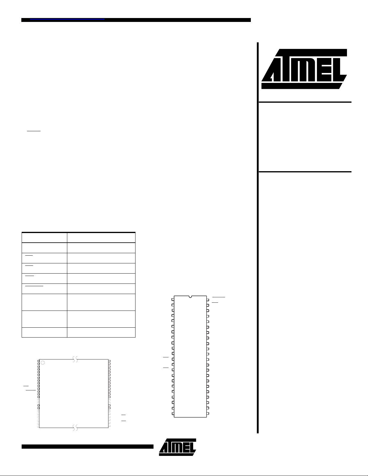
Pin Configurations
Pin Name Function
A0 - A18 Addresses
CE
Chip Enable
8-Megabit
(512K x 16)
CMOS Flash
Memory
AT49BV8192
AT49BV8192T
AT49LV8192
AT49LV8192T
OE
WE
Output Enable
Write Enable
RESET Reset
V
PP
I/O0 - I/O15
Program/Erase Power
Supply
Data
Inputs/Outputs
NC No Connect
TSOP Top View
Type 1
A15
A13
A11
A9
NC
WE
RESET
VPP
NC
A17
A6
A4
A2
1
A14
A12
A10
A8
NC
NC
A18
A7
A5
A3
A1
2
3
4
5
6
7
8
9
10
11
12
13
14
15
16
18
19 I/O8
20
21
22
23
24
SOIC (SOP)
VPP
1
2
A18
A17
3
A7
4
A6
5
A5
6
A4
7
A3
8
9
A2
10
A1
11
A0
12
NC
I/O15
I/O14
I/O13
I/O12
VCC
I/O3
I/O2
I/O1
I/O0
GND
A0
A16
GND
I/O7
I/O6
I/O5
I/O4
I/O11
I/O10
I/O9
OE
CE
48
47
46
45
44
43
42
41
40
39
38
37
36
35
34
33
3217
31
30
29
28
27
26
25
CE
GND
OE
I/O0
I/O8
I/O1
I/O9
I/O2
I/O10
I/O3
I/O11
13
14
15
16
17
18
19
20
21
22
RESET
44
WE
43
A8
42
A9
41
A10
40
A11
39
A12
38
A13
37
A14
36
A15
35
A16
34
NC
33
GND
32
31
I/O15
I/O7
30
I/O14
29
I/O6
28
I/O1327
I/O5
26
I/O1225
I/O4
24
VCC23
0978B-A–11/97
1
Page 2
The device contains a u se r-e nabl ed “ boo t b lock ” pr ote ct ion
feature. Two versions of the feature are available: the
AT49BV/LV8192 locates the boot block at lowest or der
addresses (“bottom boot ”); the AT49 BV/LV 8192T locate s it
at highest order addresses (“top boot”)
To allow for simple in-system reprogrammability, the
AT49BV/LV8192 does not require high input voltages for
programming. Reading data out of the device i s similar to
reading from an E PROM ; it h as stan dard CE
, OE, and WE
inputs to avoid bus contention. Reprogramming the
AT49BV/LV8192 is perfor med by first erasing a block of
data and then programming on a word-by-word basis.
The device is erased by executing the erase command
sequence; the device internally controls the erase operation. The memory is di vided into three bl ocks for erase
operations. There are two 8K word parameter block sections and one sector consisting of the boot block and the
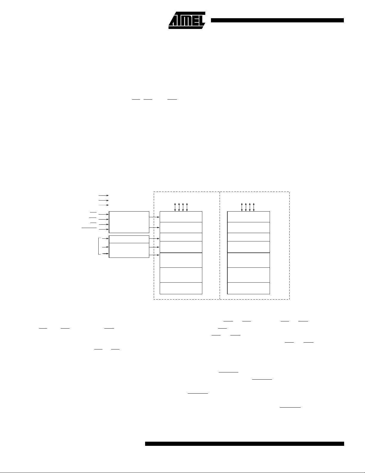
Block Diagram
V
V
GND
OE
WE
CE
RESET
ADDRESS
INPUTS
CC
PP
CONTROL
LOGIC
Y DECODER
X DECODER
AT49BV/LV8192 AT49BV/LV8192T
DATA INPUTS/OUTPUTS
I/O0 - I/O15
INPUT/OUTPUT
BUFFERS
PROGRAM DATA
LATCHES
Y-GATING
MAIN MEMORY
(488K WORDS)
PARAMETER
BLOCK 2
8K WORDS
PARAMETER
BLOCK 1
8K WORDS
BOOT BLOCK
8K WORDS
main memory array block. T he AT49BV/LV8192 is programmed on a word-by-word basis.
The device has the capability to protect the data in the boot
block; this feature is enabled by a command sequence.
Once the boot block programming lockout feature is
enabled, the data in the boot bl ock cannot be cha nged
when input levels of 3.6 volts or less are used. The typical
number of program and erase cycles is in excess of 10,000
cycles.
The optional 8K word boot block section includes a reprogramming lock o ut featur e to pro vide data i ntegrity. The
boot sector is des igned to contain us er secure code, and
when the feature is enabled, the boot sector is protected
from being reprogrammed.
During a chip erase, sector erase, or word programming,
the V
pin must be at 5V ± 10%.
PP
DATA INPUTS/OUTPUTS
I/O0 - I/O15
INPUT/OUTPUT
BUFFERS
PROGRAM DATA
LATCHES
7FFFF 7FFFF
06000
05FFF
04000
03FFF
02000
01FFF
00000 00000
Y-GATING
BOOT BLOCK
8K WORDS
PARAMETER
BLOCK 1
8K WORDS
PARAMETER
BLOCK 2
8K WORDS
MAIN MEMORY
(488K WORDS)
7E000
7DFFF
7C000
7BFFF
7A000
79FFF
Device Operation
READ:
When CE
at the memory location determined by the address pins is
asserted on the outputs . The outputs ar e put in the high
impedance state whenever CE
control gives designers flexibility in preventing bus contention.
COMMAND SEQUENCES:
ered on it will be reset to the read or standby mode
depending upon the state of the control line inputs. In order
to perform other device functions, a series of command
sequences are entered into the device. The command
sequences are shown in the Comma nd Definitions ta ble
(I/O8 - I/O15 are don't care inputs for the command codes).
The command sequences are written by applying a low
2
The AT49BV/LV8192 is access ed l ike an E PRO M .
and OE are low and WE is high, th e data sto red
or OE is high. This dual-line
When the device is first pow-
AT49BV/LV8192(T)
pulse on the WE
tively) and OE
edge of CE
latched by the first rising edge of CE
or CE input with CE or WE low (respec-
high. The address is latched on the falling
or WE, whichever occurs last. The data is
or WE. Standard
microprocessor write timings are used. The ad dress loca tions used in the command sequences are not affected by
entering the command sequences.
RESET:
A RESET
tem applications. When RESET
input pin is provided to eas e some sys-
is at a l ogic high le ve l, t he
device is in its sta nda rd ope ra tin g mo de. A lo w level on the
RESET
input halts the pre sent d evice o perati on and puts
the outputs of the de vice in a hig h impeda nce sta te. When
a high level is reas serted on the RESE T
pin, the device
returns to the Read or Standby mo de, dependi ng upon the
state of the control inputs. By applying a 12V ± 0.5V input
Page 3

AT49BV/LV8192(T)
signal to the RESET
grammed even if the boot block program lockout feature
has been enabled (see Boot Block Pro gramming Loc kout
Override section).
ERASURE:
be erased. The erased state of memory bits is a logical “1”.
The entire devi ce can be e rased by using the Chip Erase
command or indiv idual sect ors can be er ased by us ing the
Sector Erase commands.
CHIP ERASE:
time by using the 6-byte chip erase software code. After the
chip erase h as b een i ni tia ted, th e dev ice wi ll i nte rn all y ti me
the erase operation so that no external clocks are required.
The maximum time to erease the chip is t
If the boot block lockout ha s b een ena bled, th e Chip Era se
will not erase the data in the boot block; it will erase the
main memory block and the parameter blocks only. After
the chip erase, th e d ev ice will return to the r ea d or s tand by
mode.
SECTOR ERASE:
the device is organized into three sectors that can be individually erased. There are two 8K word parameter block
sections and one sector consisting of the boot block and
the main memory array blo ck. The Secto r Erase comm and
is a six bus cycle operation. The sector address is latched
on the falling WE
input command is latched at the rising edge of WE
sector erase starts after the rising edge of WE
cycle. The erase oper ation is internal ly controlled; it will
automatically time to c omple tion. W hen the b oot block programming lockout featur e is not enabled, the boot block
and the main memory block will erase together (from the
same sector erase command). Once the boot region has
been protected, only the main memory array sector will
erase when its sector erase command is issued.
WORD PROGRAMMING:
erased, it is programmed (to a logical “0”) on a word-byword basis. Programming is accomplished via the internal
device command register and is a 4 bus cycle operation.
The device will autom ati ca ll y ge nerate the required inter nal
program pulses.
Any commands written to the chip during the embedded
programming cycle will be ignored. If a hardware reset happens during programming, the data at the location being
programmed will be corrupted. Please note that a data “0”
cannot be programmed back to a “1”; only erase operations
can convert “0”s to “1”s. Programming is completed after
the specified t
also be used to indicate the end of a program cycle.
BOOT BLOCK PROGRAMMING L OCKOUT:
has one designated block that has a programming lockout
feature. This feature prevents programmi ng of data in the
designated block once the feature has been enabled. The
Before a word can be reprogrammed, it must
pin the boot block array can be repro-
The entire device can be erased at one
.
EC
As an alternative to a full chip erase,
edge of the sixth cycle while the 30H data
. The
of the si xth
Once a memory block is
cycle time. The DATA poll ing feat ure may
BP
The device
size of the block is 8K words . This bl ock, re ferre d to as the
boot block, can contain secure code that is used to bring up
the system. Enablin g the l ockout fe ature will allow t he boot
code to stay in the device while data in the rest of the
device is updated. This feature does not have to be activated; the boot block’ s u sa ge a s a write protected region is
optional to the user. The address range of the
49BV/LV8192 boot block is 00000H to 01FFFH while the
address range of the 49BV/LV8192T is 7E000H to
7FFFFH.
Once the feature is enabl ed, the da ta in the bo ot block c an
no longer be erased or programmed when input levels of
5.5V or less are u sed. Dat a in the m ain mem ory bloc k can
still be changed through the regular programming method.
To activate the lockout feature, a series of six program
commands to specific addresses with specific data must be
performed. Please refer to the Command Definitions table.
BOOT BLOCK LOCKOUT DETECTION:
method is available to determine if programming of the boot
block section is locked out. When the device is in the software product identification mode (see Software Product
Identification Entry and Exit sections) a read from address
location 00002H wil l s how i f pr ogram mi ng the b oot block is
locked out. If the data on I/O0 is low, the boot bl oc k c an be
programmed; if the data on I/O0 is high, the program lockout feature has been enabled and the bl ock ca nnot be programmed. The software product identification exit code
should be used to return to standard operation.
BOOT BLOCK PROGRAMMING LOCKOUT OVERRIDE:
The user can override the boot block programming
lockout by ta king the RES ET
entire chip eras e, s ecto r era se or wor d pr ogramm ing oper ation. When the RESET
the boot block programming lockout feature is again active.
PRODUCT IDENTIFICATION:
mode identifies the device and manufacturer as Atmel. It
may be accessed by hardware or software operation. The
hardware operation mode can be used by an external programmer to identify the correct programming algorithm for
the Atmel product.
For details, see Operating Modes (for hardware operation)
or Software Product Identification. The manufacturer and
device code is the same for both modes.
DATA POLLING:
polling to indicate the end of a program cycle. During a program cycle an attempted read of the last byte loaded will
result in the c omple ment of t he load ed data on I/O7 . Once
the program cycle has been completed, true data is valid
on all output s and the next c ycle ma y begin . Duri ng a chip
or sector erase operation, an attempt to read the device will
give a “0” on I/O7. Once the program or erase cycle has
completed, true data will be read from the device. DATA
polling may begin at any time during the program cycle.
The AT49BV/LV8192 features DATA
pin to 12 volts during the
pin is brought back to T TL levels
The product identif ication
A software
3
Page 4

TOGGLE BIT:
In addition to DATA
polling the
AT49BV/LV8192 provides another method for determining
the end of a program or erase cycle. Dur ing a program or
erase operation, successive attempts to read data from the
device will result in I/O6 toggling between one and zero.
Once the program cycle has completed, I/O6 will stop toggling and valid data will be read. Examini ng the toggle bit
may begin at any time during a program cycle.
HARDWARE DATA PROTECTION:
Hardware features
protect against inadvertent programs to the
AT49BV/LV8192 in the followin g ways: (a) V
is below 1.8V (typical), th e program func tion is inhib-
V
CC
sense: if
CC
ited. (b) V
sense level, the device will automatically time out 10
V
CC
power on delay: once VCC has reached the
CC
ms (typical) before pr ogramm ing. (c) Prog ram inhib it: hold ing any one of OE
low, CE high or WE high inhibits program cycles. (d) Noise filter: pulses of less than 15 ns (typical) on the WE
or CE inputs will not initiate a program
cycle.
INPUT LEVELS:
While operating with a 2.7V to 3.6V
power supply, th e address inp uts and con trol inputs (OE
, and WE) may be driven from 0 to 5.5V without
CE
adversely affecting the operation of the device. The I/O
lines can only be driven from 0 to V
+ 0.6V.
CC
,
4
AT49BV/LV8192(T)
Page 5

AT49BV/LV8192(T)
OUT
(1)
2nd Bus
Cycle
3rd Bus
Cycle
4th Bus
Cycle
5th Bus
Cycle
IN
6th Bus
Cycle
(4)(5)
Command Definition (in Hex)
1st Bus
Command
Sequence
Read 1 Addr D
Chip Erase 6 5555 AA 2AAA 55 5555 80 5555 AA 2AAA 55 5555 10
Sector Erase 6 5555 AA 2AAA 55 5555 80 5555 AA 2AAA 55 SA
Word Program 4 5555 AA 2AAA 55 5555 A0 Addr D
Boot Block Lockout
Product ID Entry 3 5555 AA 2AAA 55 5555 90
Product ID Exit
Product ID Exit
Notes: 1. The DATA FORMAT in each bus cycle is as follows: I/O15 - I/O8 (Don’t Care); I/O7 - I/O0 (Hex)
(3)
(3)
2. The 8K word boot se cto r ha s the address range 00000H to 01FFF H for the AT49BV/LV8192 and 7E000H to 7FF FFH for the
AT49BV/LV8192T.
3. Either one of the Product ID Exit commands can be used.
4. SA = sector addresses:
For the AT49BV/LV8192
SA = 03XXX for PARAMETER BLOCK 1
SA = 05XXX for PARAMETER BLOCK 2
SA = 7FXXX for MAIN MEMORY ARRAY
Bus
Cycles
(2)
6 5555 AA 2AAA 55 5555 80 5555 AA 2AAA 55 5555 40
3 5555 AA 2AAA 55 5555 F0
1 xxxx F0
Cycle
Addr Data Addr Data Addr Data Addr Data Addr Data Addr Data
30
For the AT49BV/LV8192T
SA = 7DXXX for PARAMETER BLOCK 1
SA = 7BXXX for PARAMETER BLOCK 2
SA = 79XXX for MAIN MEMORY ARRAY
5. When the boot block programming lockout feature is not enabled, the boot block and the main memory block will erase
together (form the same sector erase command). Once the boot region has been protected, only the main memory array
sector will erase when its sector erase command is issued.
Absolute Maximum Ratings*
Temperature Under Bias................................ -55°C to +125°C
Storage Temperature..................................... -65°C to +150°C
All Input Voltages
(including NC Pins)
with Respect to Ground...................................-0.6V to +6.25V
All Output Voltages
with Respect to Ground.............................-0.6V to V
Voltage on RESET
with Respect to Ground...................................-0.6V to +13.5V
+ 0.6V
CC
*NOTICE: Stresses beyond those listed under “Absolute
Maximum Ratings” may cause permanent damage to the dev ice . This is a s tress rating only an d
functional oper ation of the device at thes e o r any
other conditions beyond those indicated in the
operational sections of this specification is not
implied. Exposure to absolute maximum rating
conditions f or e xtended periods ma y af fect de vice
reliability .
5
Page 6

DCand AC Operating Range
Operating
Temperature (Case)
Power Supply
V
CC
Com. 0°C - 70°C 0°C - 70°C 0°C - 70°C
Ind. -40°C - 85°C -40°C - 85°C -40°C - 85°C
AT49LV8192 3.0V to 3.6V 3.0V to 3.6V 3.0V to 3.6V
AT49BV8192 2.7V to 3.6V 2.7V to 3.6V 2.7V to 3.6V
Operating Modes
AT49BV/LV8192-12 AT49BV/LV8192-15 AT49BV/LV8192-20
Mode CE OE WE RESET V
Read V
Program/Erase
(2)
Standby/Program
Inhibit
V
V
IH
V
IL
V
IL
X
Program Inhibit X X V
Program Inhibit X V
Output Disable X V
Reset X X X V
V
IL
IH
(1)
IL
IH
IH
V
IL
XVIHX X High Z
IH
XVIHV
XVIHX High Z
V
IH
V
IH
V
IH
IL
Product Identification
Hardware V
Softwar e
(5)
V
IL
V
IL
IH
V
IH
V
IH
Notes: 1. X can be VIL or VIH.
2. Refer to AC Programming Waveforms.
= 12.0V ± 0.5V.
3. V
H
4. Manufacturer Code: 1FH, Device Code: A0H (49BV/LV8192), A3H (49BV/LV8192T).
5. See details under Software Product Identification Entry/Exit.
PP
XAiD
5V ± 10% Ai D
V
IL
IL
Ai I/O
OUT
IN
X X High Z
A1 - A18 = VIL, A9 = VH,
A0 = V
A1 - A18 = VIL, A9 = VH,
A0 = V
A0 = VIL, A1 - A18 = V
A0 = VIH, A1 - A18 = V
(3)
IL
IH
IL
IL
Manufacturer Code
(3)
Devi ce Code
Manufacturer Code
Devi ce Code
(4)
(4)
(4)
(4)
DC Characteristics
Symbol Parameter Condition Min Max Units
I
LI
I
LO
I
SB1
I
SB2
(1)
I
CC
V
IL
V
IH
V
OL
V
OH
Input Load Current VIN = 0V to V
Output Leakage Current V
VCC Standby Current CMOS CE = VCC - 0.3V to V
VCC Standby Current TTL CE = 2.0V to V
V
Active Current f = 5 MHz; I
CC
Input Low Voltage 0.6 V
Input High Voltage 2.0 V
Output Low Voltage IOL = 2.1 mA 0.45 V
Output High V oltage IOH = -400 µA2.4V
Note: 1. In the erase mode, I
6
AT49BV/LV8192(T)
is 50 mA.
CC
= 0V to V
I/O
CC
CC
CC
CC
= 0 mA 25 mA
OUT
10
10
50
1mA
µ
A
µ
A
µ
A
Page 7

AC Read Characteristics
AT49BV/LV8192(T)
AT49BV/LV8192-12 AT49BV/LV8192-15 AT49BV/LV8192-20
Symbol Parameter
t
ACC
(1)
t
CE
(2)
t
OE
(3)(4)
t
DF
t
OH
Address to Output Delay 120 150 200 ns
CE to Output Delay 120 150 200 ns
OE to Output Delay 0 50 0 100 0 100 ns
CE or OE to Output Float 030050050ns
Output Hold from OE, CE
or Address, whichever occurred first
AC Read Waveforms
UnitsMin Max Min Max Min Max
000ns
(1)(2)(3)(4)
Notes: 1. CE may be delayed up to t
- tCE after the address transition without impact on t
ACC
2. OE may be delayed up to tCE - tOE after the f al lin g e dge o f CE w ithout im pact on tCE or by t
without impact on t
ACC
.
3. tDF is specified from OE or CE whichever occurs first (CL = 5 pF).
4. This parameter is characterized and is not 100% tested.
Input Test Waveforms and Measurement Level
tR, tF < 5 ns
Pin Capacitance
(f = 1 Mhz, T = 25°C)
C
IN
C
OUT
Note: 1. This parameter is characterized and is not 100% tested.
(1)
Typ Max Units Conditions
46 pFV
812 pFV
.
ACC
- tOE after an address change
ACC
Output Test Load
= 0V
IN
= 0V
OUT
7
Page 8

AC Word Load Characteristics
Symbol Parameter Min Max Units
t
, t
AS
OES
t
AH
t
CS
t
CH
t
WP
t
DS
t
, t
DH
OEH
t
WPH
AC Word Load Waveforms
Controlled
WE
Address, OE Set-up Time 10 ns
Address Hold Time 100 ns
Chip Select Set-up Time 0 ns
Chip Select Hold Time 0 ns
Write Pulse Width (WE or CE)200ns
Data Set-up Time 100 ns
Data, OE Hold Time 10 ns
Write Pulse Width High 200 ns
CE
Controlled
8
AT49BV/LV8192(T)
Page 9

AT49BV/LV8192(T)
Program Cyc le Characteristics
Symbol Parameter Min Typ Max Units
t
BP
t
AS
t
AH
t
DS
t
DH
t
WP
t
WPH
t
EC
Word Programming Time 30 µs
Address Set-up Time 0 ns
Address Hold Time 100 ns
Data Set-up Time 100 ns
Data Hold Time 0 ns
Write Pulse Width 200 ns
Write Pulse Width High 200 ns
Erase Cycle Time 10 seconds
Program Cycle Waveforms
OE
CE
WE
t
AS
AO-A18
DATA
5555 5555
PROGRAM CYCLE
t
WP
t
AH
AA
t
DH
2AAA
t
DS
55
t
WPH
ADDRESS
A0
INPUT
DATA
t
BP
5555
AA
Sector or Chip Erase Cycle Waveforms
(1)
OE
CE
t
WP
WE
AO-A18
DATA
t
AS
5555
WORD 0
t
AH
AA
t
DH
2AAA 2AAA
t
DS
55 55
WORD 1 WORD 2
Notes: 1. OE must be high only when WE and CE are both low.
2. For chip erase, the address should be 5555. For sector erase, the address depends on what sector is to be erased. (See
note 4 under command definitions.)
3. For chip erase, the data should be 10H, and for sector erase, the data should be 30H.
t
5555
WPH
5555
80
AA
WORD 3
WORD 4
Note 2
Note 3
WORD 5
t
EC
9
Page 10

Data P o lling Characteristics
(1)
Symbol Parameter Min T yp Max Units
t
t
t
t
DH
OEH
OE
WR
Data Hold Time 10 ns
OE Hold Time 10 ns
OE to Output Delay
Write Recovery Time 0 ns
(2)
Notes: 1. These parameters are characterized and not 100% tested.
2. See tOE spec in AC Read Characteristics.
Data Polling Waveforms
ns
Toggle Bit Characteristics
(1)
Symbol Parameter Min Typ Max Units
t
DH
t
OEH
t
OE
t
OEHP
t
WR
Data Hold Time 10 ns
OE Hold Time 10 ns
OE to Output Delay
OE High Pulse 150 ns
Write Recovery Time 0 ns
(2)
Notes: 1. These parameters are characterized and not 100% tested.
2. See t
Toggle Bit Waveforms
Notes: 1. Toggling either OE or CE or both OE and CE will operate toggle bit. The t
spec in AC Read Characteristics.
OE
(1)(2)(3)
specification must be met by the toggling
OEHP
input(s).
2. Beginning and ending state of I/O6 will vary.
3. Any address location may be used but the address should not vary.
ns
10
AT49BV/LV8192(T)
Page 11

AT49BV/LV8192(T)
Software Product
Identification Entry
LOAD DATA AA
ADDRESS 5555
LOAD DATA 55
ADDRESS 2AAA
LOAD DATA 90
ADDRESS 5555
ENTER PRODUCT
IDENTIFICATION
MODE
Software Product
Identifcation Exit
LOAD DATA AA
TO
ADDRESS 5555
LOAD DATA 55
TO
ADDRESS 2AAA
(1)(6)
(1)
TO
TO
TO
OR
(2)(3)(5)
LOAD DATA F0
ANY ADDRESS
EXIT PRODUCT
IDENTIFICAT ION
MODE
TO
Boot Block
Lockout Enable Algorithm
LOAD DATA AA
TO
ADDRESS 5555
LOAD DATA 55
TO
ADDRESS 2AAA
LOAD DATA 80
TO
ADDRESS 5555
LOAD DATA AA
TO
ADDRESS 5555
LOAD DATA 55
TO
ADDRESS 2AAA
LOAD DATA 40
TO
ADDRESS 5555
(4)
PAUSE 1 second
(1)
ADDRESS 5555
EXIT PRODUCT
IDENTIFICATION
Notes: 1.
LOAD DATA F0
TO
(4)
MODE
Data Format: I/O15 - I/O8 (Don’t Care); I/O7 - I/O0 (Hex)
Address Format: A14 - A0 (Hex).
2. A1 - A18 = V
Manufacture Code is read for A0 = V
Device Code is read for A0 = V
3.
The device does not remain in identification mode if powered down.
4.
The device returns to standard operation mode.
5.
Manufacturer Code: 1FH
Device Code: A0H (49BV/LV8192), A3H (49BV/LV8192T)
6.
Either one of the Product ID Exit commands can be used.
.
IL
;
IL
.
IH
Notes: 1.
Data Format: I/O15 - I/O8 (Don’t Care); I/O7 - I/O0 (Hex)
Address Format: A14 - A0 (Hex).
2.
Boot block lockout feature enabled.
11
Page 12

Ordering Information
t
ACC
(ns)
120 25 0.05 AT49BV8192-12RC
150 25 0.05 AT49BV8192-15RC
200 25 0.05 AT49BV8192-20RC
120 25 0.05 AT49LV8192-12RC
150 25 0.05 AT49LV8192-15RC
ICC (mA)
Active Standby Ordering Code Package Operation Range
AT49BV8192-12TC
AT49BV8192-12RI
AT49BV8192-12TI
AT49BV8192-15TC
AT49BV8192-15RI
AT49BV8192-15TI
AT49BV8192-20TC
AT49BV8192-20RI
AT49BV8192-20TI
AT49LV8192-12TC
AT49LV8192-12RI
AT49LV8192-12TI
AT49LV8192-15TC
44R
48T
44R
48T
44R
48T
44R
48T
44R
48T
44R
48T
44R
48T
44R
48T
44R
48T
Commercial
(0° to 70°C)
Industrial
(-40° to 85°C)
Commercial
(0° to 70°C)
Industrial
(-40° to 85°C)
Commercial
(0° to 70°C)
Industrial
(-40° to 85°C)
Commercial
(0° to 70°C)
Industrial
(-40° to 85°C)
Commercial
(0° to 70°C)
AT49LV8192-15RI
AT49LV8192-15TI
200 25 0.05 AT49LV8192-20RC
AT49LV8192-20TC
AT49LV8192-20RI
AT49LV8192-20TI
Package Type
44R 44-Lead, 0.525" Wide, Plastic Gull Wing Small Outline Package (SOIC/SOP)
48T 48-Lead, Thin Small Outline Package (TSOP)
44R
48T
44R
48T
44R
48T
Industrial
(-40° to 85°C)
Commercial
(0° to 70°C)
Industrial
(-40° to 85°C)
12
AT49BV/LV8192(T)
Page 13

Ordering Information
AT49BV/LV8192(T)
t
ACC
(ns)
120 25 0.05 AT49BV8192T-12RC
150 25 0.05 AT49BV8192T-15RC
200 25 0.05 AT49BV8192T-20RC
120 25 0.05 AT49LV8192T-12RC
150 25 0.05 AT49LV8192T-15RC
ICC (mA)
Active Standby Ordering Code Package Operation Range
AT49BV8192T-12TC
AT49BV8192T-12RI
AT49BV8192T-12TI
AT49BV8192T-15TC
AT49BV8192T-15RI
AT49BV8192T-15TI
AT49BV8192T-20TC
AT49BV8192T-20RI
AT49BV8192T-20TI
AT49LV8192T-12TC
AT49LV8192T-12RI
AT49LV8192T-12TI
AT49LV8192T-15TC
44R
48T
44R
48T
44R
48T
44R
48T
44R
48T
44R
48T
44R
48T
44R
48T
44R
48T
Commercial
(0° to 70°C)
Industrial
(-40° to 85°C)
Commercial
(0° to 70°C)
Industrial
(-40° to 85°C)
Commercial
(0° to 70°C)
Industrial
(-40° to 85°C)
Commercial
(0° to 70°C)
Industrial
(-40° to 85°C)
Commercial
(0° to 70°C)
AT49LV8192T-15RI
AT49LV8192T-15TI
200 25 0.05 AT49LV8192T-20RC
AT49LV8192T-20TC
AT49LV8192T-20RI
AT49LV8192T-20TI
Package Type
44R 44-Lead, 0.525" Wide, Plastic Gull Wing Small Outline Package (SOIC/SOP)
48T 48-Lead, Thin Small Outline Package (TSOP)
44R
48T
44R
48T
44R
48T
Industrial
(-40° to 85°C)
Commercial
(0° to 70°C)
Industrial
(-40° to 85°C)
13
 Loading...