

Datasheet AT49BV512-15VI, AT49BV512-15VC, AT49BV512-15TI, AT49BV512-15TC, AT49BV512-15PI Datasheet (ATMEL)
...Page 1
Features
•
Single Supply Voltage, Range 2.7V to 3.6V
•
Single Supply for Read and Write
•
Fast Read Access Time - 120 ns
•
Internal Program Control and Timer
•
8K bytes Boot Block With Lockout
•
Fast Erase Cycle Time - 10 seconds
•
Byte By Byte Programming - 30
•
Hardware Data Protection
•
DAT A Polling For End Of Program Detection
•
Low Power Dissipation
µµµµ
s/Byte typical
– 25 mA Active Current
µµµµ
–50
A CMOS Standby Current
•
Typical 10,000 Write Cycles
Description
The AT49BV512 is a 3-volt-only, 512K Flas h mem or ie s organized as 65,536 words of
8 bits each. Manufactured with Atmel’s advanced nonvolatile CMOS technology, the
devices offer access times to 120 ns with power di ssipation of just 9 0 mW ov er the
commercial temperature range. When the devices are deselected, the CMOS standby
current is less than 50
To allow for simple in-system reprogrammability, the AT49BV512 does not require
high input voltages for programming. Three-volt-only commands determine the read
and programming operation of the device. Reading data out of the device is similar to
reading from an EPROM. Reprogramming the AT49BV512 is performed by erasing
the entire 1 megabit of memory and then programming on a byte by byte basis. The
µµµµA.
(continued)
512K (64K x 8)
Single 2.7-volt
Battery-Voltage
Flash Memory
AT49BV512
™
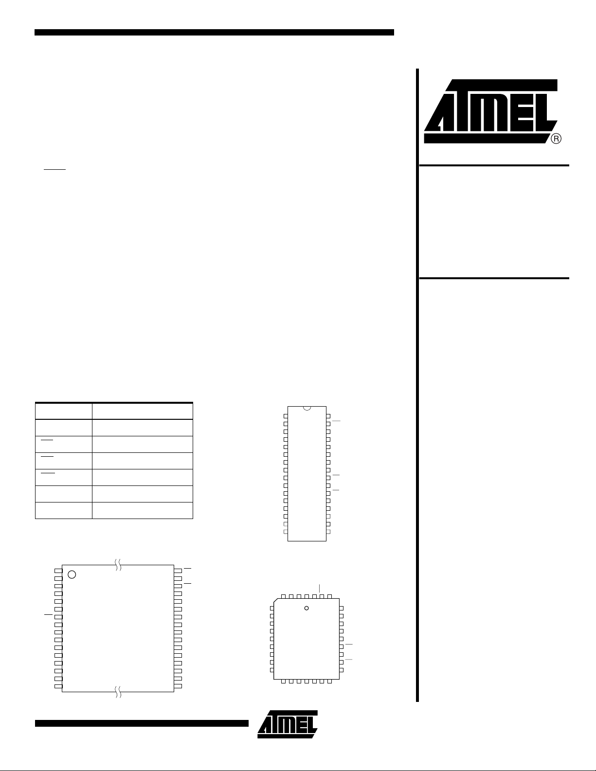
Pin Configurations
Pin Name Function
A0 - A15 Addresses
CE
OE
WE
I/O0 - I/O7 Data Inputs/Outputs
NC No Connect
VSOP Top View (8 x 14 mm) or
TSOP Top View (8 x 20 mm)
1
A11
2
A9
3
A8
4
A13
5
A14
6
NC
7
WE
8
VCC
9
NC
10
NC
11
A15
12
A12
13
A7
14
A6
15
A5
16
A4
Chip Enable
Output En able
Write Enable
Type 1
DIP Top View
1
2
3
4
5
6
7
8
9
10
11
12
13
14
15
16
A15NCNC
I/O2
GND
1
I/O3
32
31
30
29
28
27
26
25
24
23
22
21
20
19
18
17
VCCWENC
323130
I/O4
I/O5
VCC
WE
NC
A14
A13
A8
A9
A11
OE
A10
CE
I/O7
I/O6
I/O5
I/O4
I/O3
29
28
27
26
25
24
23
22
21
I/O6
A14
A13
A8
A9
A11
OE
A10
CE
I/O7
Rev. 1026C–09/98
NC
NC
A15
A12
A7
A6
A5
A4
A3
A2
A1
A0
I/O0
I/O1
I/O2
GND
OE
32
A10
31
CE
30
I/O7
29
I/O6
28
I/O5
27
I/O4
26
I/O3
25
GND
24
I/O2
23
I/O1
22
I/O0
21
A0
20
A1
19
A2
18
A3
17
PLCC Top View
A12
432
5
A7
6
A6
7
A5
8
A4
9
A3
10
A2
11
A1
12
A0
13
I/O0
14151617181920
I/O1
1
Page 2
typical byte programming time is a fast 30
program cycle can be optionally detected by the DATA
µµµµs. The end of a
polling feature. Once the end of a byte program cycle has
been detected, a new acce ss for a re ad or progr am can
begin. The typical number of program and erase cycles is
in excess of 10,000 cycles.
The optional 8K bytes boot block section includes a reprogramming write lock out feature to provide data integrity.
The boot sector is desig ned to contai n user secure code,
and when the featur e is e nabled , th e boot sector is pe rmanently protected from being reprogrammed.
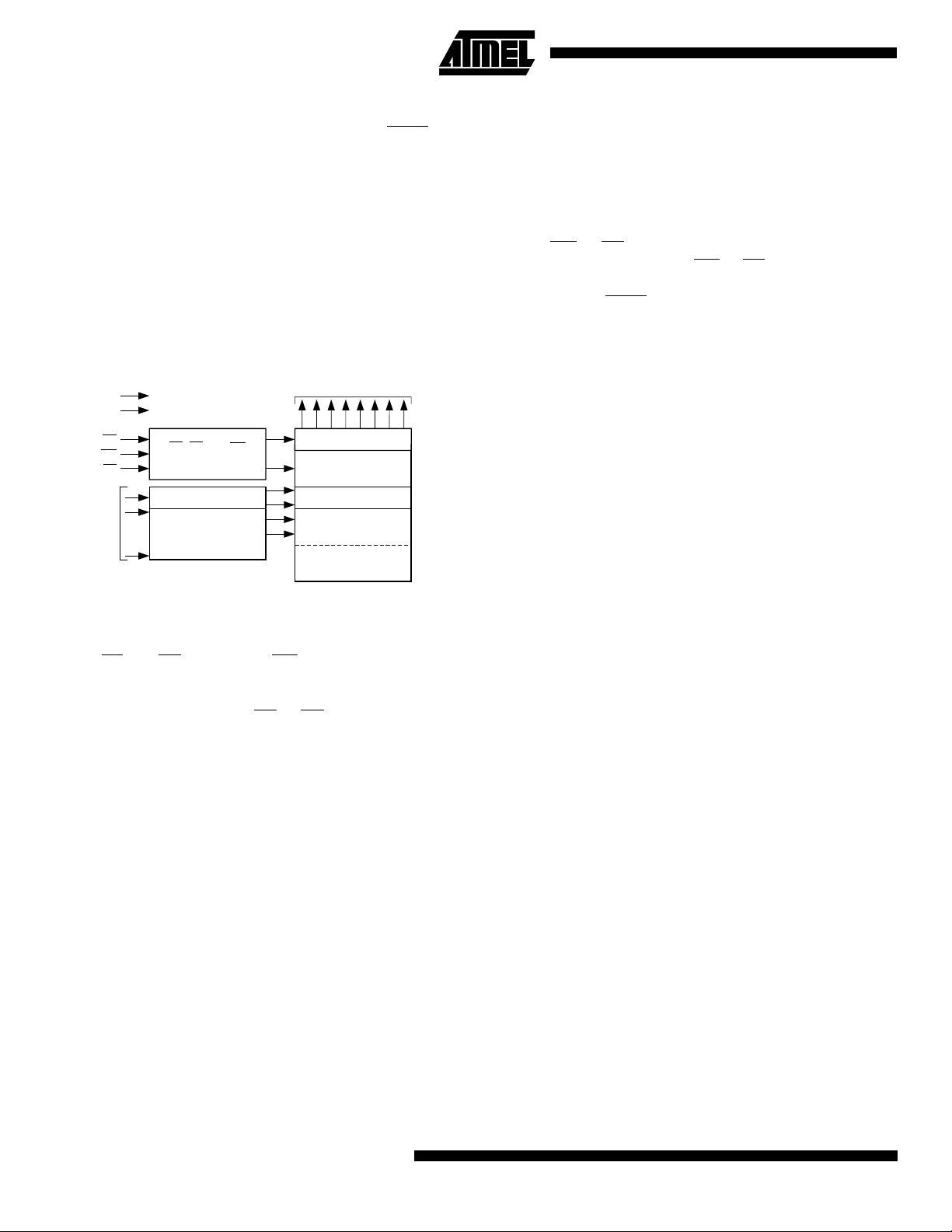
Block Diagram
DATA INPUTS/OUTPUTS
VCC
GND
OE
WE
CE
ADDRESS
INPUTS
OE, CE AND WE
LOGIC
Y DECODER
X DECODER
I/O0 - I/O7
DATA LATCH
INPUT/OUTPUT
BUFFERS
Y-GATING
MAIN MEMORY
(56K BYTES)
OPTIONAL BOOT
BLOCK (8K BYTES)
FFFFH
2000H
1FFFH
0000H
Device Operation
READ:
When CE
at the memory location determined by the address pins is
asserted on the outputs. The outputs are put in the high
impedance state whenever CE
line control gives designers flexibility in preventing bus contention.
ERASURE:
bytes memory array (or 56K bytes if the boot block featured
is used) must be erased. The erased state of the memory
bits is a logical “1”. The entire device can be erased at one
time by using a 6-byte software code. The software chip
erase code consists of 6-byte load commands to specific
address locat ions with a s pecif ic data patte rn (plea se refer
to the Chip Erase Cycle Waveforms).
After the software chip erase has been ini tiated , the devi ce
will internally time the eras e operatio n so that no ex ternal
clocks are required . The ma ximum tim e needed to erase
the whole chip is t
been enabled, the data in the boot sector will not be
erased.
BYTE PROGRAMMING:
erased, the device is programmed (to a logical “0”) on a
byte-by-byte basis. Please note that a data “0” cannot be
The AT49BV512 is accessed like an EPROM.
and OE are low and WE is high, the data stored
or OE is high. This dual-
Before a byte can be reprogrammed, the 64K
. If the boot block lockout feature has
EC
Once the memory array is
programmed ba ck to a “1”; only era se oper ation s can con vert “0”s to “1”s. Programming is accomplished via the
internal device command register and is a 4 bus cycle operation (please refer to the Com mand Definitions table). The
device will automatically generate the required internal program pulses.
The program cycle has addresses latched on the falling
edge of WE
latched on the rising edge of WE
first. Programming is c ompleted after the sp ecified t
or CE, whichever occurs last, and the data
or CE, whichever occurs
BP
cycle time. The DATA poll ing featu re may al so be use d to
indicate the end of a program cycle.
BOOT BLOCK PROGRAMMING LOCKOUT:
The device
has one designated block that has a programming lockout
feature. This feature prevents programming of data in the
designated block once the fe ature has be en enable d. The
size of the block is 8 K bytes. Thi s block, referred to as the
boot block, can contain secure code that is used to bring up
the system. Enabling the lockout feature will allow the boot
code to stay in the device while data in the rest of the
device is updated. This fe ature do es not have to be activated; the boot block’ s u sa ge a s a write protected region is
optional to the user. The address range of the boot block is
0000H to 1FFFH.
Once the feature is enabl ed, the da ta in the bo ot block c an
no longer be erased or programmed. Data i n the main
memory block can still be changed through the regular programming method. To activate the lockout feature, a series
of six program commands to spec ific addresses wi th specific data must be performed. Please refer to the Command Definitions table.
BOOT BLOC K LOCKOUT DET ECTION:
A software
method is available to determine if programming of the boot
block section is l ocked out. W hen the device is in the sof tware product identification mode (see Software Product
Identification Entry and Exit sections) a read from address
location 00002H wil l s how i f pr ogram mi ng the b oot block is
locked out. If the data on I/O0 is low, the boot block can be
programmed; if the data on I/O0 is high, the program lockout feature has been activated and the block cannot be
programmed. The software product i dentification code
should be used to return to standard operation.
PRODUCT IDENTIFICATION:
The product identif ication
mode identifies the device and manufac turer as Atmel. It
may be accessed by hardwar e or softwar e operatio n. The
hardware operation mode can be used by an external programmer to identify the correct programming algorithm for
the Atmel product.
For details, see Operating Modes (for hardware operation)
or Software Product Identification. The manufacturer and
device code is the same for both modes.
2
AT49BV512
Page 3
AT49BV512
DATA POLLING:
The AT49BV512 features DATA
polling
to indicate the end of a program cycle. Dur ing a program
cycle an attempted read of the last byte loaded will result in
the complement of the loaded data on I/O 7. Once the program cycle has been com pleted, true data is valid on all
outputs and the next cycle may begin . DATA
polling may
begin at any time during the program cycle.
TOGGLE BIT:
In addition to DATA
polling the AT49 BV512
provides another method for determining the end of a program or erase cycle. During a prog ra m or era se oper ati on ,
successive attempts to read data from the device will result
in I/O6 toggling between one and zero. Once the program
cycle has completed, I/O6 will stop toggling and valid data
HARDWARE DATA PROTECTION:
Hardware features
protect against inadvertent programs to the AT49BV512 in
the following ways: (a) V
sense: if VCC is below 1.8V
CC
(typical), the program function is inhibited. (b) Program
inhibit: holding any one of OE
low, CE high or WE high
inhibits program cycles. (c) Noise filter: Pulses of less than
15 ns (typical) on the WE
or CE inputs will not i ni t ia t e a pro-
gram cycle.
INPUT LEVELS:
While operating with a 2.7V to 3.6V
power supply, th e address inp uts and con trol inputs (OE
and WE) may be driven from 0 to 5.5V without
CE
adversely affecting the operation of the devic e. The I/O
lines can only be driven from 0 to V
+ 0.6V.
CC
will be read. Examinin g the toggl e bit may begin at a ny
time during a program cycle.
Command Definition (in Hex)
1st Bus
Command
Sequence
Read 1 Addr D
Chip Erase 6 5555 AA 2AAA 55 5555 80 5555 AA 2AAA 55 5555 10
Byte
Program
Bus
Cycles
4 5555 AA 2AAA 55 5555 A0 Addr D
Cycle
Addr Data Addr Data Addr Data Addr Data Addr Data Addr Data
OUT
2nd Bus
Cycle
3rd Bus
Cycle
4th Bus
Cycle
5th Bus
Cycle
IN
6th Bus
Cycle
,
Boot Block
Lockout
Product ID
Entry
Product ID
Exit
Product ID
Exit
Notes: 1. The 8K byte boot sector has the address range 0000H to 1FFFH.
(1)
(2)
(2)
2. Either one of the Product ID exit commands can be used.
6 5555 AA 2AAA 55 5555 80 5555 AA 2AAA 55 5555 40
3 5555 AA 2AAA 55 5555 90
3 5555 AA 2AAA 55 5555 F0
1 XXXX F0
Absolute Maximum Ratings*
Temperature Under Bias............................. ..-55°C to +125°C
Storage Temperature.....................................-65°C to +150°C
All Input Voltages
(including NC Pins)
with Respect to Ground...................................-0.6V to +6.25V
All Output Voltages
with Respect to Ground.............................-0.6V to V
Voltage on OE
with Respect to Ground...................................-0.6V to +13.5V
+ 0.6V
CC
*NOTICE: Stresses beyond those listed under “Absolute
Maximum Ratings” may cause permanent damage to the dev ice . This is a s tress rating only an d
functional oper ation of the de vice at these or any
other conditions beyond those indicated in the
operational sections of this specification is not
implied. Exposure to absolute maximum rating
conditions f or e xtended periods ma y af fect de vice
reliability .
3
Page 4
DC and AC Operating Range
AT49BV512-12 AT49BV512-15
Com. 0°C - 70°C0°C - 70°C
Operating Temperature (Case)
Ind. -40°C - 85°C-40°C - 85°C
V
Power Supply 2.7V to 3.6V 2.7V to 3.6V
CC
Operating Modes
Mode CE OE WE Ai I/O
Read V
Program
(2)
Standby/Write Inhibit V
IL
V
IL
IH
X
V
IL
V
IH
(1)
Program Inhibit X X V
Program Inhibit X V
Output Disable X V
IL
IH
Product Identification
Hardware V
Software
(5)
IL
V
IL
Notes: 1. X can be VIL or VIH.
2. Refer to AC Programming Waveforms.
= 12.0V ± 0.5V.
3. V
H
4. Manufacturer Code: 1FH, Device Code: 03H.
5. See details under Software Product Identification Entry/Exit.
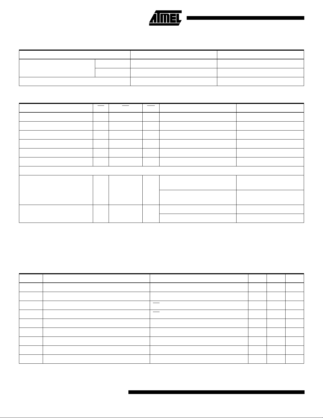
DC Characteristics
V
IH
V
IL
Ai D
Ai D
OUT
IN
XXHigh Z
IH
X
XHigh Z
V
IH
A1 - A15 = VIL, A9 = VH,
A0 = V
IL
A1 - A15 = VIL, A9 = VH,
A0 = V
IH
A0 = VIL, A1 - A15 = V
A0 = VIH, A1 - A15 = V
(3)
(3)
IL
IL
Manufacturer Code
Device Code
Manufacturer Code
Device Code
(4)
(4)
(4)
(4)
Symbol Parameter Condition Min Max Units
I
LI
I
LO
I
SB1
I
SB2
(1)
I
CC
V
IL
V
IH
V
OL
V
OH
Input Load Current VIN = 0V to V
Output Leakage Current V
VCC Standby Current CMOS CE = V
= 0V to V
I/O
CC
- 0.3V to V
VCC Standby Current TTL CE = 2.0V to V
V
Active Current f = 5 MHz; I
CC
OUT
CC
CC
CC
CC
= 0 mA 25 mA
10 µA
10 µA
50 µA
1mA
Input Low Voltage 0.6 V
Input High Voltage 2.0 V
Output Low Voltage IOL = 2.1 mA 0.45 V
Output High Voltage IOH = -100 µA; VCC = 3.0V 2.4 V
Note: 1. In the erase mode, ICC is 50 mA.
4
AT49BV512
Page 5

AC Read Characteristics
,
100 pF
1.3K
1.8K
3.0V
OUTPUT
PIN
Symbol Parameter
t
ACC
t
CE
tOE
t
DF
t
OH
(1)
(2)
(3, 4)
Address to Output Delay 120 150 ns
CE to Output Delay 120 150 ns
OE to Output Delay 50 0 70 ns
CE or OE to Output Float 0 30 0 40 ns
Output Hold from OE, CE or Address, whic hever occurred first 0 0 ns
AT49BV512
AT49BV512-12 AT49BV512-15
UnitsMin Max Min Max
AC Read Waveforms
(1)(2)(3)(4)
ADDRESS
CE
OE
OUTPUT
Notes: 1. CE may be delayed up to t
ACC
2. OE may be delayed up to tCE - tOE after the falling edge of CE with out im pa ct on tCE or by t
without impact on t
is specified from OE or CE whichever occurs frist (CL - 5 pF).
3. t
DF
ACC
.
4. This parameter is characterized and is not 100% tested.
Input Test Waveforms and
Measurement Level
AC
DRIVING
LEVELS
t
tF < 5 ns
R
2.4V
1.5V
0.4V
ADDRESS VALID
tCE
tACC
HIGH Z
tOH
OUTPUT VALID
- tCE after the address transition without impact on t
Output Test Load
AC
MEASUREMENT
LEVEL
ACC
tDF
.
- tOE after an address change
ACC
Pin Capacitance
f = 1 MHz, T = 25°C
C
IN
C
OUT
Note: 1. This parameter is characterized and is not 100% tested.
(1)
Ty p Max Units Conditions
46pFV
812pFV
IN
OUT
= 0V
= 0V
5
Page 6

AC Byte Load Characteristics
Symbol Parameter Min Max Units
tAS, t
OES
t
AH
t
CS
t
CH
t
WP
t
DS
tDH, t
OEH
t
WPH
Address, OE Set-up Time 0 ns
Address Hold Time 100 ns
Chip Select Set-up Time 0 ns
Chip Select Hold Time 0 ns
Write Pulse Width (WE or CE)200ns
Data Set-up Time 100 ns
Data, OE Hold Time 0 ns
Write Pulse Width High 200 ns
AC Byte Load Waveforms
WE Controlled
OE
CE Controlled
ADDRESS
CE
WE
DATA IN
OE
ADDRESS
WE
tAS
tCS
tAS
tCS
tOES
tOES
tAH
tWP tWPH
tDS tDH
tAH
tOEH
tCH
tOEH
tCH
CE
tWP tWPH
tDS tDH
DATA IN
6
AT49BV512
Page 7

AT49BV512
Program Cyc le Characteristics
Symbol Parameter Min Typ Max Units
t
BP
t
AS
t
AH
t
DS
t
DH
t
WP
t
WPH
t
EC
Program Cycle Waveforms
Byte Programming Time 30 µs
Address Set-up Time 0 ns
Address Hold Time 100 ns
Data Set-up Time 100 ns
Data Hold Time 0 ns
Write Pulse Width 200 ns
Write Pulse Width High 200 ns
Erase Cycle Time 10 seconds
PROGRAM CYCLE
OE
CE
WE
tAS
A0-A15
DATA
5555 2AAA 5555
AA 55 A0
Chip Erase Cycle Waveforms
OE
CE
tWP
WE
tAH
tDS
AA 55 80
BYTE 0 BYTE 1 BYTE 2 BYTE 3 BYTE 4 BYTE 5
A0-A15
DATA
tAS
5555 2AAA 5555
tWP
tAH
tDS
tWPH
tDH
tWPH
tDH
ADDRESS
INPUT
DATA
5555 2AAA 5555
AA 55 10
tBP
tEC
Note: OE must be high only when WE and CE are both low.
7
Page 8

Data Po lling Characteristics
(1)
Symbol Parameter Min Typ Max Units
t
DH
t
OEH
t
OE
t
WR
Data Hold Time 0 ns
OE Hold Time 10 ns
OE to Output Delay
(2)
Write Recovery Time 0 ns
Notes: 1. These parameters are characterized and not 100% tested.
2. See tOE spec in AC Read Characteristics.
Data Polling Waveforms
WE
CE
tOEH
OE
tDH
I/O7
tOE
tWR
ns
A0-A15
Toggle Bit Characteristics
(1)
An
An An AnAn
Symbol Parameter Min Typ Max Units
t
DH
t
OEH
t
OE
t
OEHP
t
WR
Data Hold Time 0 ns
OE Hold Time 10 ns
OE to Output Delay
(2)
ns
OE High Pulse 150 ns
Write Recovery Time 0 ns
Notes: 1. These parameters are characterized and not 100% tested.
2. See tOE spec in AC Read Characteristics.
WE
CE
OE
I/O6
(1)(2)(3)
tOEH
tDH
tOEHP
tOE
tWR
HIGH Z
Toggle Bit Waveforms
Notes: 1. Toggling either OE or CE or both OE and CE will operate toggle bit. The t
input(s).
2. Beginning and ending state of I/O6 will vary.
3. Any address location may be used but the address should not vary.
8
AT49BV512
specification must be met by the toggling
OEHP
Page 9

AT49BV512
LOAD DATA AA
TO
ADDRESS 5555
LOAD DATA 55
TO
ADDRESS 2AAA
LOAD DATA 80
TO
ADDRESS 5555
LOAD DATA AA
TO
ADDRESS 5555
LOAD DATA 55
TO
ADDRESS 2AAA
LOAD DATA 40
TO
ADDRESS 5555
PAUSE 1 second
(2)
Software Product
Identification Entry
LOAD DATA AA
ADDRESS 5555
LOAD DATA 55
ADDRESS 2AAA
LOAD DATA 90
ADDRESS 5555
ENTER PRODUCT
IDENTIFICATION
MODE
Software Product
Identification Exit
(1)
(1)
TO
TO
TO
(2)(3)(5)
Boot Block Lockout Feature
Enable Algorithm
(1)
LOAD DATA AA
TO
ADDRESS 5555
Notes: 1. Data Format: I/O7 - I/O0 (Hex);
LOAD DATA 55
TO
ADDRESS 2AAA
LOAD DATA F0
TO
ADDRESS 5555
EXIT PRODUCT
IDENTIFICATION
MODE
(4)
Address Format: A14 - A0 (Hex).
2. A1 - A15 = V
OR
.
IL
Manufacture Code is read for A0 = V
Device Code is read for A0 = V
3. The device does note remain in identification mode
if powered down.
4. The device returns to standard operation mode.
5. Manufacturers Code: 1FH
Device Code: 03H.
LOAD DATA F0
TO
ANY ADDRESS
EXIT PRODUCT
IDENTIFICATION
MODE
IH
(4)
IL
.
Notes: 1. Data Format: I/O7 - I/O0 (Hex);
Address Format: A14 - A0 (Hex).
2. Boot block lockout feature enabled.
;
9
Page 10

Ordering Information
I
(mA)
t
ACC
(ns)
120 25 0.05 AT49BV512-12JC
150 25 0.05 AT49BV512-15JC
Note: 1. The AT49BV512 has as optional boot block feature. The part number shown in the Ordering Information table is for devices
with the boot block in the lower address range (i.e., 0000H to 1FFFH). Users requiring boot block protection to be in the
higher address range should contact Atmel.
CC
25 0.05 AT49BV512-12JI
25 0.05 AT49BV512-15JI
(1)
Ordering Code Package Operation RangeActive Standby
AT49BV512-12PC
AT49BV512-12TC
AT49BV512-12VC
AT49BV512-12PI
AT49BV512-12TI
AT49BV512-12VI
AT49BV512-15PC
AT49BV512-15TC
AT49BV512-15VC
AT49BV512-15PI
AT49BV512-15TI
AT49BV512-15VI
32J
32P6
32T
32V
32J
32P6
32T
32V
32J
32P6
32T
32V
32J
32P6
32T
32V
Commercial
(0°C - 70°C)
Industrial
(-40°C - 85°C)
Commercial
(0°C - 70°C)
Industrial
(-40°C - 85°C)
Package Type
32J 32-Lead, Plastic J-Leaded Chip Carrier Package (PLCC)
32P6 32-Lead, 0.600" Wide, Plastic Dual Inline Package (PDIP)
32T 32-Lead, Thin Small Outline Package (TSOP) (8 x 20 mm)
32V 32-Lead, Thin Small Outline Package (VSOP) (8 x 14 mm)
10
AT49BV512
Page 11

Packaging Information
AT49BV512
32J
, 32-Lead, Plastic J-Leaded Chip Carrier (PLCC)
Dimensions in Inches and (Millimeters)
.045(1.14) X 45°
.032(.813)
.026(.660)
.050(1.27) TYP
.453(11.5)
.447(11.4)
.495(12.6)
.485(12.3)
PIN NO.1
IDENTIFY
.553(14.0)
.547(13.9)
.300(7.62) REF
.430(10.9)
.390(9.90)
.025(.635) X 30° - 45°
.595(15.1)
.585(14.9)
AT CONTACT
POINTS
.022(.559) X 45° MAX (3X)
.012(.305)
.008(.203)
.021(.533)
.013(.330)
.030(.762)
.015(3.81)
.095(2.41)
.060(1.52)
.140(3.56)
.120(3.05)
.530(13.5)
.490(12.4)
32P6
, 32-Lead, 0.600” Wide, Plastic Dual Inline
Package (PDIP)
Dimensions in Inches and (Millimeters)
1.67(42.4)
.220(5.59)
SEATING
PLANE
MAX
.161(4.09)
.125(3.18)
.110(2.79)
.090(2.29)
.012(.305)
.008(.203)
1.64(41.7)
1.500(38.10) REF
.065(1.65)
.041(1.04)
.630(16.0)
.590(15.0)
.690(17.5)
.610(15.5)
PIN
0
REF
15
1
.566(14.4)
.530(13.5)
.090(2.29)
.005(.127)
.065(1.65)
.015(.381)
.022(.559)
.014(.356)
MAX
MIN
32T
, 32-Lead, Plastic Thin Small Outline Package
(TSOP) Dimensions in Millimeters and (Inches)*
JEDEC OUTLINE MO-142 BD
INDEX
MARK
0.50(.020)
BSC
0
REF
5
7.50(.295)
REF
8.20(.323)
7.80(.307)
0.15(.006)
0.05(.002)
18.5(.728)
18.3(.720)
0.25(.010)
0.15(.006)
0.70(.028)
0.50(.020)
20.2(.795)
19.8(.780)
1.20(.047) MAX
0.20(.008)
0.10(.004)
*Controlling dimensions: millimeters
32V
, 32-Lead, Plastic Thin Small Outline Package
(VSOP)
Dimensions in Millimeters (Inches)
INDEX
MARK
0.50(.020)
BSC
0
REF
5
7.50(.295)
REF
8.10(.319)
7.90(.311)
0.15(.006)
0.05(.002)
12.5(.492)
12.3(.484)
0.25(.010)
0.15(.006)
0.70(.028)
0.50(.020)
14.2(.559)
13.8(.543)
1.20(.047) MAX
0.20(.008)
0.10(.004)
11
 Loading...