

Page 1
Up to 6 GHz Medium Power
Silicon Bipolar Transistor Chip
Technical Data
AT-42000
Features
• High Output Power:
21.0 dBm Typical P
20.5 dBm Typical P
• High Gain at 1 dB
Compression:
15.0 dB Typical G
10.0 dB Typical G
• Low Noise Figure: 1.9 dB
Typical NFO at 2.0 GHz
• High Gain-Bandwidth
Product: 9.0 GHz Typical f
at 2.0␣ GHz
1 dB
at 4.0␣ GHz
1 dB
at 2.0␣ GHz
1 dB
at 4.0␣ GHz
1 dB
T
Description
Hewlett-Packard’s AT-42000 is a
general purpose NPN bipolar
transistor chip that offers excellent high frequency performance.
The 4 micron emitter-to-emitter
pitch enables this transistor to be
used in many different functions.
The 20 emitter finger interdigitated
geometry yields a medium sized
transistor with impedances that
are easy to match for low noise
and medium power applications.
This device is designed for use in
low noise, wideband amplifier,
mixer and oscillator applications
in the VHF, UHF, and microwave
frequencies. An optimum noise
match near 50 Ω up to 1 GHz ,
makes this device easy to use as a
low noise amplifier.
The AT-42000 bipolar transistor is
fabricated using Hewlett-Packard’s
10 GHz f
(SAT) process. The die is nitride
passivated for surface protection.
Excellent device uniformity,
performance and reliability are
produced by the use of ionimplantation, self-alignment
techniques, and gold metalization
in the fabrication of this device.
The recommended assembly
procedure is gold-eutectic die
attach at 400oC and either wedge
or ball bonding using 0.7 mil gold
wire. See APPLICATIONS section,
“Chip Use”.
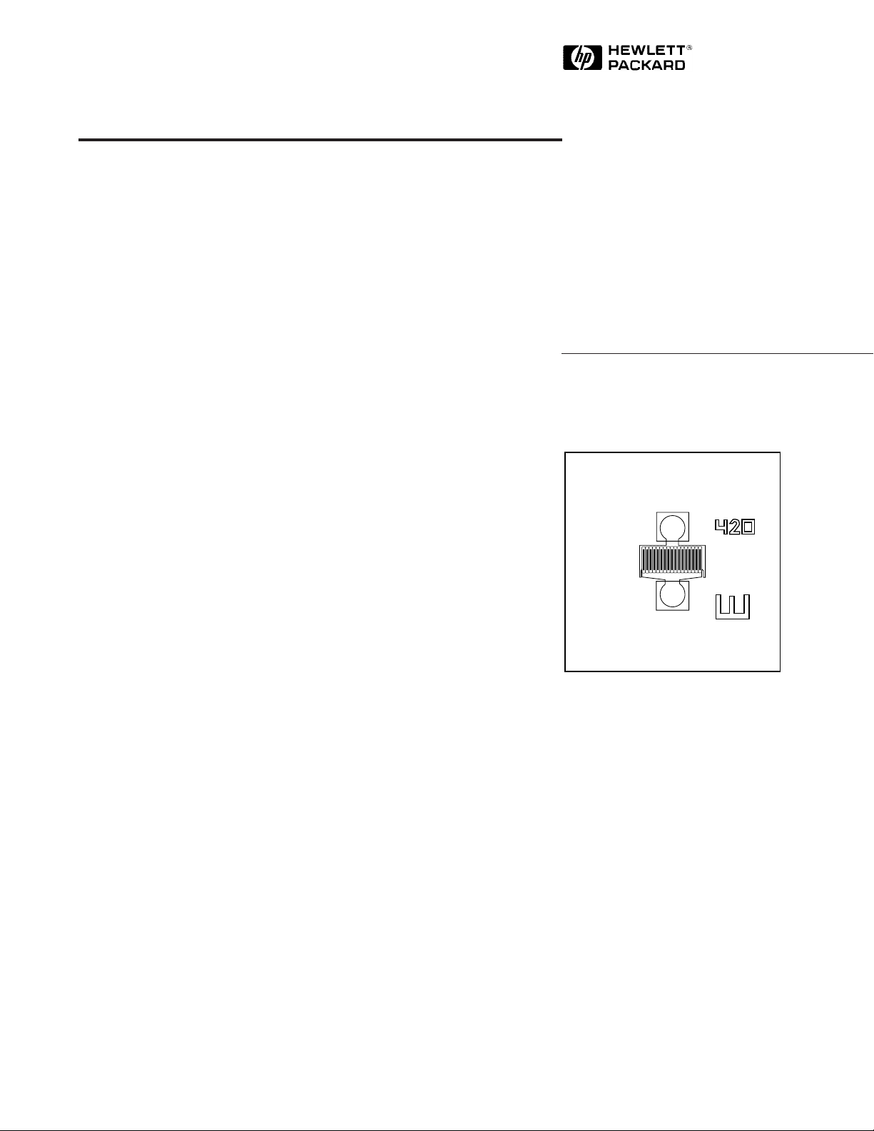
Self-Aligned-Transistor
T
Chip Outline
4-149
5965-8909E
Page 2
AT-42000 Absolute Maximum Ratings
Absolute
Symbol Parameter Units Maximum
V
V
V
T
EBO
CBO
CEO
I
C
P
T
STG
T
j
Emitter-Base Voltage V 1.5
Collector-Base Voltage V 20
Collector-Emitter Voltage V 12
Collector Current mA 80
Power Dissipation
[2,3]
m W 600
Junction Temperature °C 200
Storage Temperature °C -65 to 200
Part Number Ordering Information
Part Number Devices Per Tray
AT-42000-GP4 100
[1]
Thermal Resistance
[2,4]
θjc = 70°C/W
Notes:
1. Permanent damage may occur if
any of these limits are exceeded.
2. T
Mounting Surface
3. Derate at 14.3 mW/° C for
T
Mounting Surface
4. The small spot size of this technique results in a higher, though
more accurate determination of θ
than do alternate methods. See
MEASUREMENTS section
“Thermal Resistance” for more
information.
= 25°C.
> 158° C.
:
jc
Electrical Specifications, T
Symbol Parameters and Test Conditions
|S
|2Insertion Power Gain; VCE = 8 V, IC = 35 mA f = 2.0 GHz dB 11.5
21E
= 25° C
A
[1]
Units Min. Typ. Max.
f = 4.0 GHz 5.5
P
1 dB
Power Output @ 1 dB Gain Compression f = 2.0 GHz dBm 21.0
VCE = 8 V, IC = 35 mA f= 4.0 GHz 20.5
G
1 dB
1 dB Compressed Gain; VCE = 8 V, IC = 35 mA f = 2.0 GHz dB 15.0
f = 4.0 GHz 10.0
NF
Optimum Noise Figure: VCE = 8 V, IC = 10 mA f = 2.0 GHz dB 1.9
O
f = 4.0 GHz 3.0
G
A
Gain @ NFO; VCE = 8 V, IC = 10 mA f = 2.0 GHz dB 14.0
f = 4.0 GHz 10.5
f
T
h
FE
I
CBO
I
EBO
C
CB
Notes:
1.
RF performance is determined by packaging and testing 10 devices per wafer
2. For this test, the emitter is grounded.
Gain Bandwidth Product: VCE = 8 V, IC = 35 mA GHz 9.0
Forward Current Transfer Ratio; VCE = 8 V, IC = 35 mA — 30 150 270
Collector Cutoff Current; V
Emitter Cutoff Current; V
Collector Base Capacitance
= 8 V µA 0.2
CB
= 1 V µA 2.0
EB
[2]
: VCB = 8 V , f = 1 MH z pF 0.23
.
4-150
Page 3

AT-42000 Typical Performance, T
FREQUENCY (GHz)
Figure 5. Insertion Power Gain,
Maximum Available Gain and
Maximum Stable Gain vs. Frequency.
V
CE
= 8 V, IC = 35 mA.
GAIN (dB)
0.1 0.50.3 1.0 3.0 6.0
IC (mA)
Figure 1. Output Power and 1 dB
Compressed Gain vs. Collector
Current and Frequency. V
CE
= 8 V.
24
20
16
12
8
4
G
1 dB
(dB) P
1 dB
(dBm)
0 1020304050
P
1dB
G
1dB
2.0 GHz
2.0 GHz
4.0 GHz
4.0 GHz
40
35
30
25
20
15
10
5
0
MSG
MAG
|S
21E
|
2
IC (mA)
Figure 3. Insertion Power Gain vs.
Collector Current and Frequency.
V
CE
= 8 V.
20
16
12
8
4
0
|S
21E
|
2
GAIN (dB)
0 1020304050
1.0 GHz
2.0 GHz
4.0 GHz
IC (mA)
Figure 2. Output Power and 1 dB
Compressed Gain vs. Collector
Current and Voltage. f = 2.0 GHz.
10 V
4 V
6 V
4 V
10 V
6 V
24
20
16
12
16
14
12
10
G
1 dB
(dB) P
1 dB
(dBm)
0 1020304050
P
1dB
G
1dB
FREQUENCY (GHz)
Figure 6. Noise Figure and Associated
Gain vs. Frequency.
V
CE
= 8 V, IC = 10mA.
GAIN (dB)
24
21
18
15
12
9
6
3
0
4
3
2
1
0
NF
O
(dB)
0.5 2.01.0 3.0 4.0 5.0
G
A
NF
O
IC (mA)
Figure 4. Insertion Power Gain vs.
Collector Current and Voltage.
f = 2.0 GHz.
13
12
11
10
9
8
7
|S
21E
|
2
GAIN (dB)
0 1020304050
10 V
6 V
4 V
= 25° C
A
4-151
Page 4

AT-42000 Typical Scattering Parameters,
Common Emitter, Z
Freq. S
GHz Mag. Ang. dB Mag. Ang. dB Mag. Ang. Mag. Ang.
0.1 .70 -50 28.0 25.19 155 -37.7 .013 71 .92 -14
0.5 .67 -136 20.9 11.04 108 -30.5 .030 43 .57 -27
1.0 .66 -166 15.7 6.08 90 -28.9 .036 47 .50 -24
1.5 .66 -173 12.1 4.02 86 -28.2 .039 52 .48 -23
2.0 .66 179 9.8 3.09 82 -27.5 .042 57 .47 -23
2.5 .67 170 7.8 2.46 74 -26.0 .050 66 .47 -23
3.0 .67 165 6.3 2.08 68 -24.7 .058 72 .47 -26
3.5 .70 157 5.1 1.80 61 -23.4 .068 77 .47 -28
4.0 .70 151 3.9 1.56 57 -21.8 .081 82 .48 -30
4.5 .71 145 2.9 1.40 51 -20.7 .092 86 .50 -34
5.0 .73 138 1.9 1.24 41 -19.3 .109 87 .51 -38
5.5 .74 132 1.2 1.15 36 -17.2 .138 88 .51 -50
6.0 .76 129 0.2 1.02 32 -16.3 .154 87 .53 -56
= 50 Ω, TA=25°C, V
O
11
=8 V, IC␣=␣ 10 mA
CE
S
21
S
12
S
AT-42000 Typical Scattering Parameters,
Common Emitter, Z
Freq. S
GHz Mag. Ang. dB Mag. Ang. dB Mag. Ang. Mag. Ang.
0.1 .49 -96 33.0 44.61 143 -40.9 .009 65 .79 -24
0.5 .62 -163 22.8 13.87 98 -34.4 .019 58 .42 -26
1.0 .63 179 17.2 7.25 86 -30.5 .030 70 .38 -22
1.5 .63 171 13.5 4.74 78 -27.7 .041 76 .38 -23
2.0 .65 163 11.2 3.62 72 -25.4 .054 79 .38 -25
2.5 .65 159 9.3 2.90 67 -23.6 .066 82 .38 -27
3.0 .68 154 7.8 2.44 60 -22.1 .079 82 .38 -29
3.5 .67 148 6.5 2.12 57 -20.6 .093 84 .39 -32
4.0 .69 144 5.3 1.83 51 -19.7 .104 86 .40 -34
4.5 .70 139 4.4 1.65 47 -18.3 .121 86 .41 -40
5.0 .70 137 3.3 1.46 43 -17.5 .133 85 .42 -44
5.5 .72 131 2.7 1.36 38 -16.5 .149 86 .41 -48
6.0 .74 128 1.7 1.22 34 -15.7 .164 85 .44 -55
A model for this device is available in the DEVICE MODELS section.
= 50 Ω, TA=25°C, V
O
11
=8 V, IC␣=␣ 35 mA
CE
S
21
S
12
S
22
22
AT-42000 Noise Parameters: V
Freq. NF
GHz dB
0.1 1.0 .04 13 0.13
0.5 1.1 .05 69 0.13
1.0 1.5 .09 127 0.12
2.0 1.9 .23 171 0.11
4.0 3.0 .47 -154 0.14
O
Mag Ang
= 8 V, IC = 10 mA
CE
Γ
opt
4-152
RN/50
Page 5

AT-42000 Chip Dimensions
Base Pad
30 µm
1.18 mil
DIA
90 µm
3.54 mil
Emitter Pad
Note: Die thickness is 5 to 6 mil.
305 µm
12 mil
305 µm
12 mil
4-153
 Loading...