

Page 1
Low Cost General Purpose
Transistors
Technical Data
AT-41586
Features
• Low Noise Figure
1.4 dB Typical at 1 GHz
1.7 dB Typical at 2 GHz
• High Associated Gain
17.0 dB Typical at 1 GHz
12.5 dB Typical at 2 GHz
• Low Cost Surface Mount
Package
• Tape and Reel Option
Available
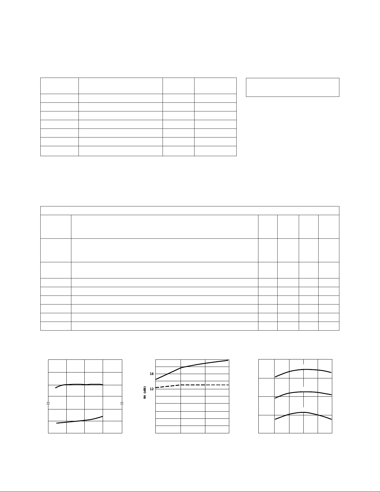
24
21
18
15
12
A
G (dB)
9
6
3
0
0.5
Figure 1. AT-41586 Noise Figure and
Associated Gain vs. Frequency at
VCE = 8 V, IC= 10 mA.
G
A
NF
O
FREQUENCY (GHz)
4.01.0
3.02.0
Description
Hewlett-Packard’s AT-41586 is a
general purpose NPN bipolar
transistor that offers excellent
high frequency performance. The
AT-41586 is housed in a low cost
surface mount .085" diameter
plastic package. The 4 micron
emitter-to-emitter pitch enables
this transistor to be used in many
different functions. The 14 emitter
finger interdigitated geometry
yields an intermediate sized
transistor with impedances that
are easy to match for low noise
and moderate power applications.
Applications include use in
wireless systems as an LNA, gain
stage, buffer, oscillator, and
mixer. An optimum noise match
near 50 Ω in the 1 to 2 GHz
frequency range, makes this
4
device easy to use as a low noise
amplifier.
O
2
NF (dB)
0
The AT-41586 bipolar transistor is
fabricated using Hewlett-Packard’s
10 GHz fT Self-Aligned-Transistor
(SAT) process. The die is nitride
passivated for surface protection.
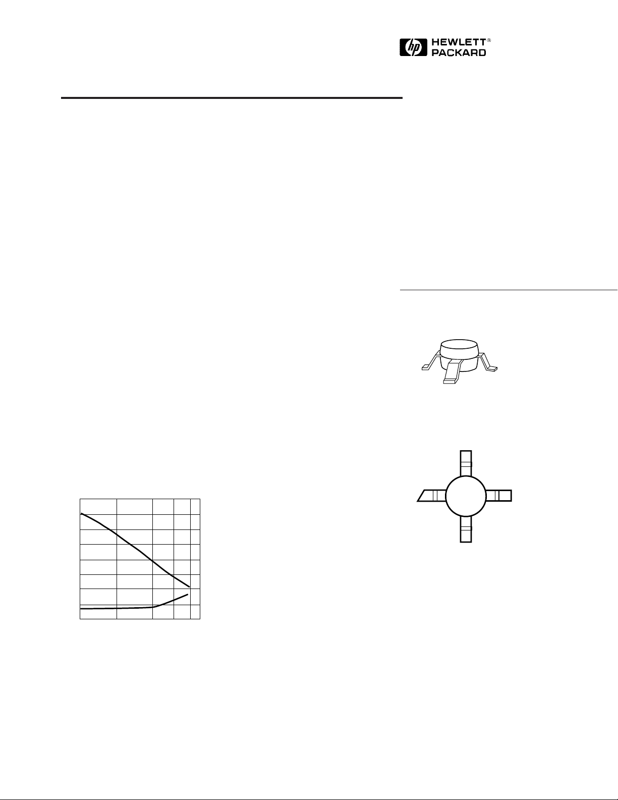
86 Plastic Package
Pin Connections
EMITTER
4
BASE
1
415
2
EMITTER
Excellent device uniformity,
performance and reliability are
produced by the use of ionimplantation, self-alignment
techniques, and gold metalization
in the fabrication of this device.
COLLECTOR
3
5965-8908E
4-144
Page 2
AT-41586 Absolute Maximum Ratings
[1]
Absolute
Symbol Parameter Units Maximum
V
EBO
V
CBO
V
CEO
I
C
P
T
T
j
T
STG
Notes:
1. Operation of this device above any one of these parameters may cause permanent damage.
2. T
= 25°C.
CASE
3. See MEASUREMENTS section, “Thermal Resistance,” for more information.
Emitter-Base Voltage V 1.5
Collector-Base Voltage V 20
Collector-Emitter Voltage V 12
Collector Current mA 60
Power Dissipation
[2]
mW 500
Junction Temperature °C 150
Storage Temperature °C -65 to 150
[1]
Thermal Resistance:
θ
=165°C/W
jc
[3]
Electrical Specifications, T
= 25° C, V
A
= 8 V
CE
Symbol Parameters and Test Conditions Unit Min. Typ. Max.
NF
Optimum Noise Figure: IC = 10 mA f = 1.0 GHz dB 1.4
o
f = 2.0 GHz 1.7
f = 4.0 GHz 3.0
G
Gain @ NF0: IC = 10 mA f = 1.0 GHz dB 17.0
A
f = 2.0 GHz 12.5
f = 4.0 GHz 8.0
2
|S
|
21E
Insertion Power Gain: IC = 25 mA f = 1.0 GHz dB 17.0
f = 2.0 GHz 11.0
P
1dB
G
1dB
f
T
h
FE
I
CBO
I
EBO
Note:
1. For more information on outlines 86, refer to “Tape and Reel Packaging for Surface Mount Devices.”
16
14
A
G (dB)
12
10
030
Figure 2. AT-41586 Optimum Noise
Figure and Associated Gain vs. Collector Current at VCE = 8 V, f = 2.0 GHz.
Power Output @ 1 dB Gain Compression: IC = 25 mA f = 2.0 GHz dBm 18.0
1 dB Compressed Gain: IC = 25 mA f = 2.0 GHz dB 13.0
Gain Bandwidth Product: IC = 25 mA GHz 8.0
Forward Current Transfer Ratio: IC = 10 mA 30 150 270
Collector Cutoff Current: V
Emitter Cutoff Current: V
G
A
NF
O
10 20
I (mA)
C
4
2
0
= 8 V µA 0.2
CB
= 1 V µA 1.0
EB
20
18
P
1dB
16
14
G
1dB
12
10
GAIN (dB)
8
6
4
O
2
NF (dB)
0
10 20
COLLECTOR CURRENT
Figure 3. AT-41586 P
Collector Current at VCE = 8 V,
1dB
f␣ =␣ 2.0␣ GHz.
30
and G
1dB
40
vs.
20
1.0 GHz
15
I (mA)
C
2.0 GHz
4.0 GHz
2
10
21E
|S | (dB)
5
0
02540
510
Figure 4. AT-41586 Insertion Power
Gain vs. Collector Current and
Frequency at 25°C, V
CE
= 8 V.
30
4-145
Page 3

AT-41586 Typical Scattering Parameters at T
VCE = 8 V, IC = 10 mA, Z
Frequency
= 50 Ω
o
S
11
S
21
= 25° C
A
S
12
(GHz) Mag. Ang. (dB) Mag. Ang. (dB) Mag. Ang. Mag. Ang.
0.100 0.78 -39 28.4 26.3 154 -36.4 0.015 71 0.91 -16
0.200 0.71 -71 26.9 22.1 134 -31.7 0.026 59 0.79 -27
0.300 0.65 -95 25.2 18.1 122 -29.8 0.032 50 0.67 -34
0.400 0.61 -113 23.5 15.0 119 -28.8 0.036 44 0.58 -38
0.500 0.59 -127 22.0 12.6 114 -28.1 0.039 43 0.52 -40
0.600 0.57 -137 20.7 10.8 100 -27.5 0.042 43 0.47 -40
0.700 0.56 -146 19.6 9.5 95 -27.1 0.044 43 0.44 -41
0.800 0.56 -154 18.5 8.4 91 -26.5 0.047 43 0.42 -41
0.900 0.55 -160 17.6 7.6 86 -26.1 0.049 44 0.40 -42
1.000 0.55 -166 16.8 6.9 83 -25.8 0.051 47 0.38 -42
1.500 0.55 173 13.4 4.7 70 -23.8 0.064 49 0.34 -45
2.000 0.57 157 10.9 3.5 57 -22.0 0.079 49 0.32 -52
2.500 0.59 144 9.2 2.9 44 -20.6 0.093 48 0.31 -61
3.000 0.62 133 7.6 2.4 34 -19.3 0.108 47 0.30 -71
3.500 0.64 123 6.0 2.0 25 -18.1 0.124 45 0.30 -83
4.000 0.67 114 5.1 1.8 16 -17.0 0.141 42 0.31 -95
4.500 0.70 106 4.1 1.6 5 -15.9 0.159 39 0.32 -108
5.000 0.73 99 2.9 1.4 -3 -15.0 0.176 35 0.32 -121
5.500 0.76 93 1.6 1.2 -8 -14.2 0.193 31 0.34 -135
6.000 0.78 88 0.8 1.1 -18 -13.5 0.209 31 0.36 -150
S
22
AT-41586 Typical Noise Parameters at T
Z
= 50 Ω, I
O
Frequency NF
(GHz) (dB) Mag. Ang. R
= 10 mA, V
C
CE
= 8 V
O
Γ
opt
0.1 1.3 0.12 3 0.17
0.5 1.3 0.10 16 0.17
1.0 1.4 0.04 43 0.16
2.0 1.7 0.12 -145 0.16
= 25° C,
C
/50 Ω
N
35
30
25
20
15
GAIN (dB)
10
5
0
0.1
Figure 5. AT-41586 Insertion Power
Gain, Maximum Available Gain and
Maximum Stable Gain vs. Frequency
at VCE = 8 V, IC = 10 mA.
|S |
21E
MSG
2
MAG
FREQUENCY (GHz)
6.01.0
4-146
Page 4

AT-41586 Typical Scattering Parameters at T
VCE = 8 V, IC = 25 mA, Z
Frequency
= 50 Ω
o
S
11
S
21
= 25° C
A
S
12
(GHz) Mag. Ang. (dB) Mag. Ang. (dB) Mag. Ang. Mag. Ang.
0.100 0.64 -61 31.9 39.4 154 -37.0 0.014 64 0.82 -24
0.200 0.59 -101 29.2 28.7 169 -33.1 0.022 53 0.64 -35
0.300 0.56 -125 26.6 21.4 124 -31.7 0.026 49 0.53 -38
0.400 0.55 -140 24.6 17.0 111 -30.4 0.030 49 0.47 -39
0.500 0.54 -151 22.9 14.0 104 -29.6 0.033 50 0.43 -38
0.600 0.54 -159 21.4 11.7 97 -28.8 0.036 52 0.40 -38
0.700 0.54 -166 20.1 10.1 91 -28.1 0.039 53 0.40 -37
0.800 0.54 -171 19.0 8.9 86 -27.5 0.042 55 0.38 -37
0.900 0.54 -176 18.0 7.9 81 -26.9 0.045 56 0.37 -37
1.000 0.55 177 17.1 7.2 77 -26.3 0.048 57 0.36 -37
1.500 0.57 164 13.6 4.8 64 -23.8 0.064 59 0.34 -42
2.000 0.57 152 11.1 3.6 55 -21.9 0.080 57 0.32 -49
2.500 0.60 141 9.2 2.9 44 -20.0 0.100 55 0.31 -58
3.000 0.62 132 7.6 2.4 34 -18.4 0.120 52 0.31 -68
3.500 0.64 124 6.4 2.1 24 -17.0 0.140 49 0.31 -80
4.000 0.67 116 5.6 1.9 18 -14.8 0.180 45 0.32 -94
4.500 0.70 109 4.1 1.6 9 -15.9 0.160 45 0.30 -109
5.000 0.73 102 3.5 1.5 1 -15.3 0.170 42 0.30 -123
5.500 0.77 96 2.3 1.3 -7 -14.4 0.190 38 0.32 -138
6.000 0.76 90 1.6 1.2 -14 -13.9 0.200 33 0.35 -152
S
22
Outline 86 Dimensions
0.51 ± 0.13
1.52 ± 0.25
(0.060 ± 0.010)
0.66 ± 0.013
(0.026 ± 0.005)
0.30 MIN
(0.012 MIN)
(0.020 ± 0.005)
45°
(0.105 ± 0.15)
DIMENSIONS ARE IN MILLIMETERS (INCHES)
4
1
2
2.67 ± 0.38
5° TYP.
2.16 ± 0.13
(0.085 ± 0.005)
AT-41586 Ordering Information
C
L
3
2.34 ± 0.38
(0.092 ± 0.015)
0.203 ± 0.051
(0.006 ± 0.002)
8° MAX
0° MIN
Part Number Increment Comments
AT-41586-BLK 100 Bulk
AT-41586-TR1 1000 7 " Reel
4-147
Page 5

Device Orientation
REEL
CARRIER
TAPE
USER
FEED
DIRECTION
COVER TAPE
Tape Dimensions and Product Orientation
t
COVER
TAPE
K
T P
CAVITY
PERFORATION
CARRIER TAPE
COVER TAPE
DISTANCE
BETWEEN
CENTERLINE
P
D
0
0
10 PITCHES CUMULATIVE
P
2
TOLERANCE ON TAPE ±0.2 MM
E
A
C
DESCRIPTION SYMBOL SIZE (mm) SIZE (INCHES)
LENGTH
WIDTH
DEPTH
PITCH
BOTTOM HOLE DIAMETER
DIAMETER
PITCH
POSITION
WIDTH
THICKNESS
WIDTH
TAPE THICKNESS
CAVITY TO PERFORATION
(WIDTH DIRECTION)
CAVITY TO PERFORATION
(LENGTH DIRECTION)
B
1
A
6.45 ± 0.10
0
5.13 ± 0.10
B
0
2.11 ± 0.10
K
0
8.00 ± 0.10
P
1
1.50 min.
D
1
D
1.50 + 0.10/-0
0
4.00 ± 0.10
P
0
1.75 ± 0.10
E
W
8.00 ± 0.30
t
0.255 ± 0.013
C
9.19 ± 0.10
T
0.051 ± 0.010
t
F
5.51 ± 0.05
P
2.00 ± 0.05
2
F
W
D
1
0.254 ± 0.004
0.202 ± 0.004
0.083 ± 0.004
0.315 ± 0.004
0.059 min.
0.059 + 0.004/-0
0.157 ± 0.004
0.069 ± 0.004
0.315 ± 0.012
0.0100 ± 0.0005
0.362 ± 0.004
0.0020 ± 0.0004
0.217 ± 0.002
0.079 ± 0.002
USER FEED
DIRECTION
4-148
 Loading...