

Page 1

Up to 6 GHz Low Noise
Silicon␣ Bipolar Transistor
Technical Data
AT-41486
Features
• Low Noise Figure:
1.4 dB Typical at 1.0␣ GHz
1.7 dB Typical at 2.0␣ GHz
• High Associated Gain:
18.0 dB Typical at 1.0␣ GHz
13.0 dB Typical at 2.0␣ GHz
• High Gain-Bandwidth
Product: 8.0 GHz Typical f
T
• Surface Mount Plastic
Package
• Tape-and-Reel Packaging
Option Available
Note:
1. Refer to “Tape-and-Reel Packaging for
Semiconductor Devices”.
[1]
Description
Hewlett-Packard’s AT-41486 is a
general purpose NPN bipolar
transistor that offers excellent
high frequency performance. The
AT-41486 is housed in a low cost
surface mount .085" diameter
plastic package. The 4 micron
emitter-to-emitter pitch enables
this transistor to be used in many
different functions. The 14 emitter
finger interdigitated geometry
yields an intermediate sized
transistor with impedances that
are easy to match for low noise
and moderate power applications.
Applications include use in
wireless systems as an LNA, gain
stage, buffer, oscillator, and
mixer. An optimum noise match
near 50 Ω at 900 MHz, makes this
device easy to use as a low noise
amplifier.
The AT-41486 bipolar transistor is
fabricated using Hewlett-Packard’s
10 GHz fT Self-Aligned-Transistor
(SAT) process. The die is nitride
passivated for surface protection.
Excellent device uniformity,
performance and reliability are
produced by the use of ionimplantation, self-alignment
techniques, and gold metalization
in the fabrication of this device.
86 Plastic Package
Pin Connections
EMITTER
4
BASE
1
414
2
EMITTER
COLLECTOR
3
4-129
5965-8928E
Page 2
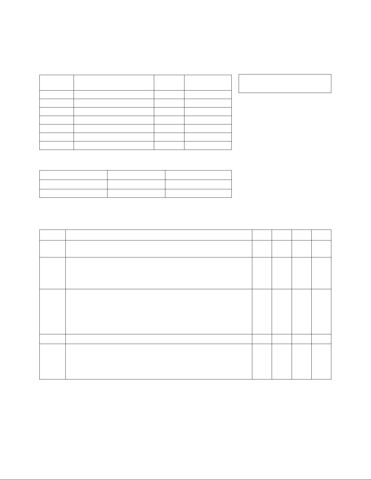
AT-41486 Absolute Maximum Ratings
Absolute
Symbol Parameter Units Maximum
V
V
V
T
EBO
CBO
CEO
I
C
P
T
STG
T
j
Emitter-Base Voltage V 1.5
Collector-Base Voltage V 20
Collector-Emitter Voltage V 12
Collector Current mA 60
Power Dissipation
[2,3]
m W 500
Junction Temperature °C 150
Storage Temperature °C -65 to 150
[1]
Part Number Ordering Information
Part Number Increment Comments
AT-41486-TR1 1000 Reel
AT-41486-BLK 100 Bulk
Note: For more information, see “Tape and Reel Packaging for Semiconductor Devices”.
Thermal Resistance
[2,4]
θjc = 165°C/W
Notes:
1. Permanent damage may occur if
any of these limits are exceeded.
2. T
3. Derate at 6 mW/° C for
4. See MEASUREMENTS section
= 25° C.
CASE
T
> 68° C.
C
“Thermal Resistance” for more
information.
:
Electrical Specifications, T
= 25° C
A
Symbol Parameters and Test Conditions Units Min. Typ. Max.
|S
|2Insertion Power Gain; VCE = 8 V, IC = 25 mA f = 2.0 GHz dB 17.5
21E
f = 4.0 GHz 11.5
P
1 dB
Power Output @ 1 dB Gain Compression f = 2.0 GHz dBm 18.0
VCE = 8 V, IC = 25 mA
G
NF
1 dB
1 dB Compressed Gain; VCE = 8 V, IC = 25 mA f = 2.0 GHz dB 13.5
Optimum Noise Figure: VCE = 8 V, IC = 10 mA f = 1.0 GHz dB 1.4 1.8
O
f = 2.0 GHz 1.7
f = 4.0 GHz 3.0
G
A
Gain @ NFO; VCE = 8 V, IC = 10 mA f = 1.0 GHz dB 17.0 18.0
f = 2.0 GHz 13.0
f = 4.0 GHz 9.0
f
T
h
FE
I
CBO
I
EBO
C
CB
Note:
1. For this test, the emitter is grounded.
Gain Bandwidth Product: VCE = 8 V, IC = 25 mA GHz 8.0
Forward Current Transfer Ratio; VCE = 8 V, IC = 10 mA — 30 150 270
Collector Cutoff Current; V
Emitter Cutoff Current; V
Collector Base Capacitance
= 8 V µA 0.2
CB
= 1 V µA 1.0
EB
[1]
: VCB = 8 V, f = 1 MHz pF 0.25
4-130
Page 3

AT-41486 Typical Performance, T
FREQUENCY (GHz)
Figure 1. Noise Figure and Associated
Gain vs. Frequency.
V
CE
= 8 V, IC = 10mA.
GAIN (dB)
IC (mA)
Figure 2. Optimum Noise Figure and
Associated Gain vs. Collector Current
and Collector Voltage. f = 2.0 GHz.
GAIN (dB)
0 10203040
Figure 3. Optimum Noise Figure and
Associated Gain vs. Collector Current
and Frequency. V
CE
= 8 V.
10 V
4 V
FREQUENCY (GHz)
Figure 5. Insertion Power Gain,
Maximum Available Gain and
Maximum Stable Gain vs. Frequency.
V
CE
= 8 V, IC = 25 mA.
GAIN (dB)
0.1 0.50.3 1.0 3.0 6.0
I
C
(mA)
GAIN (dB)
IC (mA)
Figure 4. Output Power and 1 dB
Compressed Gain vs. Collector
Current and Frequency. V
CE
= 8 V,
f = 2.0 GHz.
24
20
16
12
8
4
G
1 dB
(dB) P
1 dB
(dBm)
0 10203040
P
1dB
G
1dB
24
21
18
15
12
9
6
3
0
8
6
4
2
0
NF (dB)
4
3
2
1
NF
O
(dB)
0.5 2.01.0 3.0 4.0 5.0
15
14
13
12
11
G
A
G
A
NF
O
NF
O
G
A
NF
O
NF
50 Ω
6 V
0 10203040
2.0 GHz
2.0 GHz
4.0 GHz
4.0 GHz
6
4
2
0
NF
O
(dB)
16
14
12
10
8
IC (mA)
Figure 6. Insertion Power Gain vs.
Collector Current and Frequency.
V
CE
= 8 V.
20
16
12
8
4
0
|S
21E
|
2
GAIN (dB)
0 10203040
1.0 GHz
2.0 GHz
4.0 GHz
40
35
30
25
20
15
10
5
0
MSG
MAG
|S
21E
|
2
10 V
4 V
6 V
= 25° C
A
4-131
Page 4

AT-41486 Typical Scattering Parameters, Common Emitter,
Z
= 50 Ω, TA=25°C, V
O
Freq. S
=8 V, IC␣=␣ 10 mA
CE
11
S
21
S
12
S
GHz Mag. Ang. dB Mag. Ang. dB Mag. Ang. Mag. Ang.
0.1 .74 -38 28.1 25.46 157 -39.6 .011 68 .94 -12
0.5 .59 -127 22.0 12.63 107 -30.2 .031 47 .60 -29
1.0 .56 -168 16.8 6.92 84 -27.7 .041 46 .49 -29
1.5 .57 169 13.5 4.72 69 -26.2 .049 49 .45 -32
2.0 .62 152 11.1 3.61 56 -24.8 .058 43 .42 -39
2.5 .63 142 9.3 2.91 47 -23.4 .068 52 .40 -42
3.0 .64 130 7.6 2.41 37 -22.2 .078 52 .39 -50
3.5 .68 122 6.3 2.06 26 -20.6 .093 51 .37 -60
4.0 .71 113 5.1 1.80 16 -19.5 .106 48 .35 -70
4.5 .74 105 4.0 1.59 7 -18.0 .125 48 .35 -84
5.0 .77 99 3.1 1.42 -4 -17.2 .139 43 .35 -98
5.5 .79 93 2.0 1.27 -13 -16.3 .153 38 .35 -114
6.0 .81 87 1.1 1.13 -22 -15.4 .170 34 .35 -131
AT-41486 Typical Scattering Parameters,
Common Emitter, Z
Freq. S
GHz Mag. Ang. dB Mag. Ang. dB Mag. Ang. Mag. Ang.
0.1 .50 -75 32.0 40.01 142 -41.3 .009 54 .85 -17
0.5 .55 -158 23.2 14.38 97 -34.1 .020 48 .51 -24
1.0 .57 177 17.5 7.50 78 -29.9 .032 61 .46 -24
1.5 .57 161 14.1 5.07 65 -27.3 .043 62 .44 -28
2.0 .59 148 11.5 3.75 53 -24.8 .058 59 .43 -35
2.5 .61 139 9.6 3.02 45 -22.9 .072 58 .40 -41
3.0 .65 128 8.0 2.52 34 -21.6 .083 57 .38 -49
3.5 .70 121 6.7 2.17 24 -20.1 .099 56 .36 -59
4.0 .74 113 5.7 1.92 14 -18.8 .115 52 .34 -72
4.5 .78 107 4.7 1.72 3 -17.6 .132 47 .32 -87
5.0 .78 102 3.7 1.53 -8 -16.6 .149 42 .31 -106
5.5 .78 96 2.7 1.36 -19 -15.4 .169 36 .31 -125
6.0 .76 91 1.6 1.21 -29 -14.5 .188 31 .33 -144
A model for this device is available in the DEVICE MODELS section.
= 50 Ω, TA=25°C, V
O
11
=8 V, IC␣=␣ 25 mA
CE
S
21
S
12
S
22
22
AT-41486 Noise Parameters: V
Freq. NF
GHz dB
0.1 1.3 .12 3 0.17
0.5 1.3 .10 16 0.17
1.0 1.4 .04 43 0.16
2.0 1.7 .12 -145 0.16
4.0 3.0 .44 -99 0.40
O
Mag Ang
= 8 V, IC = 10 mA
CE
Γ
opt
4-132
RN/50
Page 5

86 Plastic Package Dimensions
0.51 ± 0.13
(0.020 ± 0.005)
4
1.52 ± 0.25
(0.060 ± 0.010)
0.66 ± 0.013
(0.026 ± 0.005)
0.30 MIN
(0.012 MIN)
45°
1
2
2.67 ± 0.38
(0.105 ± 0.15)
5° TYP.
2.16 ± 0.13
(0.085 ± 0.005)
DIMENSIONS ARE IN MILLIMETERS (INCHES)
C
L
3
2.34 ± 0.38
(0.092 ± 0.015)
0.203 ± 0.051
(0.006 ± 0.002)
8° MAX
0° MIN
4-133
 Loading...