

Page 1

Features
• Fast Read Access Time – 45 ns
• Low-Power CMOS Operation
– 100 µA Max Standby
– 20 mA Max Active at 5 MHz
• JEDEC Standard Packages
– 28-lead PDIP
– 32-lead PLCC
– 28-lead TSOP and SOIC
• 5V ± 10% Supply
• High Reliability CMOS Technology
– 2,000V ESD Protection
– 200 mA Latchup Immunity
• Rapid Programming Algorithm – 100 µs/Byte (Typical)
• CMOS and TTL Compatible Inputs and Outputs
• Integrated Product Identification Code
• Industrial and Automotive Temperature Ranges
• Green (Pb/Halide-free) Packaging Option
1. Description
The AT27C256R is a low-power, high-performance 262,144-bit one-time programmable read-only memory (OTP EPROM) organized 32K by 8 bits. It requires only one 5V
power supply in normal read mode operation. Any byte can be accessed in less than
45 ns, eliminating the need for speed reducing WAIT states on high-performance
microprocessor systems.
256K (32K x 8)
OTP EPROM
AT27C256R
Atmel’s scaled CMOS technology provides low-active power consumption, and fast
programming. Power consumption is typically only 8 mA in Active Mode and less than
10 µA in Standby.
The AT27C256R is available in a choice of industry-standard JEDEC-approved one
time programmable (OTP) plastic DIP, PLCC, SOIC, and TSOP packages. All devices
feature two-line control (CE
contention.
With 32K byte storage capability, the AT27C256R allows firmware to be stored reliably and to be accessed by the system without the delays of mass storage media.
Atmel’s AT27C256R has additional features to ensure high quality and efficient production use. The Rapid Programming Algorithm reduces the time required to program
the part and guarantees reliable programming. Programming time is typically only
100 µs/byte. The Integrated Product Identification Code electronically identifies the
device and manufacturer. This feature is used by industry-standard programming
equipment to select the proper programming algorithms and voltages.
, OE) to give designers the flexibility to prevent bus
0014K–EPROM–10/05
Page 2

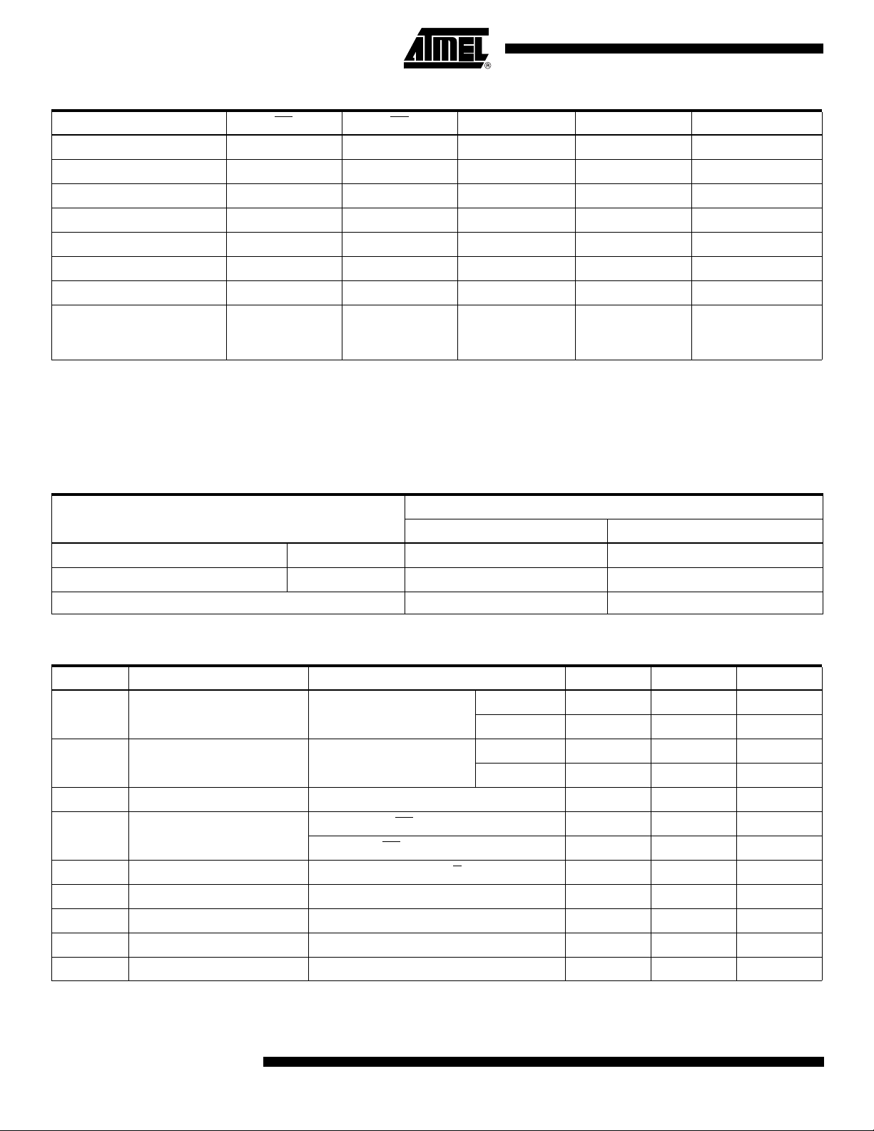
2. Pin Configurations
Pin Name Function
A0 - A14 Addresses
O0 - O7 Outputs
CE
Chip Enable
OE
Output Enable
NC No Connect
2.1 28-lead PDIP/SOIC Top View
VPP
A12
A7
A6
A5
A4
A3
A2
A1
A0
O0
O1
O2
GND
1
2
3
4
5
6
7
8
9
10
11
12
13
14
28
VCC
27
A14
26
A13
25
A8
24
A9
23
A11
22
OE
21
A10
20
CE
19
O7
18
O6
17
O5
16
O4
15
O3
2.3 28-lead TSOP Top View – Type 1
2.2 32-lead PLCC Top View
OE
A11
A9
A8
A13
A14
VCC
VPP
A12
A7
A6
A5
A4
A3
1
2
3
4
5
6
7
8
9
10
11
12
13
14
28
A10
27
CE
26
O7
25
O6
24
O5
23
O4
22
O3
21
GND
20
O2
19
O1
18
O0
17
A0
16
A1
15
A2
A7
A12
VPPNCVCC
A14
A13
432
1
O2
GND
323130
O3O4O5
NC
29
A8
28
A9
27
A11
26
NC
25
OE
24
A10
23
CE
22
O7
21
O6
A6
A5
A4
A3
A2
A1
A0
NC
O0
5
6
7
8
9
10
11
12
13
14151617181920
O1
Note: PLCC Package Pins 1 and 17 are Don’t Connect.
2
AT27C256R
0014K–EPROM–10/05
Page 3

3. System Considerations
Switching between active and standby conditions via the Chip Enable pin may produce transient voltage excursions. Unless accommodated by the system design, these transients may
exceed datasheet limits, resulting in device non-conformance. At a minimum, a 0.1 µF high
frequency, low inherent inductance, ceramic capacitor should be utilized for each device. This
capacitor should be connected between the V
to the device as possible. Additionally, to stabilize the supply voltage level on printed circuit
boards with large EPROM arrays, a 4.7 µF bulk electrolytic capacitor should be utilized, again
connected between the V
close as possible to the point where the power supply is connected to the array.
4. Block Diagram
AT27C256R
and Ground terminals of the device, as close
CC
and Ground terminals. This capacitor should be positioned as
CC
5. Absolute Maximum Ratings*
Temperature Under Bias................................ -55°C to +125°C
Storage Temperature..................................... -65°C to +150°C
Voltage on Any Pin with
Respect to Ground .........................................-2.0V to +7.0V
Voltage on A9 with
Respect to Ground ......................................-2.0V to +14.0V
VPP Supply Voltage with
Respect to Ground .......................................-2.0V to +14.0V
Note: 1. Minimum voltage is -0.6V DC which may undershoot to -2.0V for pulses of less than 20 ns. Maximum output pin voltage is
V
+ 0.75V dc which may overshoot to +7.0 volts for pulses of less than 20 ns.
CC
(1)
(1)
(1)
*NOTICE: Stresses beyond those listed under “Absolute Maxi-
mum Ratings” may cause permanent damage to
the device. This is a stress rating only and functional operation of the device at these or any other
conditions beyond those indicated in the operational sections of this specification is not implied.
Exposure to absolute maximum rating conditions
for extended periods may affect device reliability.
0014K–EPROM–10/05
3
Page 4
6. Operating Modes
Mode/Pin CE OE Ai V
Read V
Output Disable V
Standby V
Rapid Program
PGM Verify
Optional PGM Verify
PGM Inhibit
Product Identification
(2)
(2)
(2)
(2)
(4)
X
IL
IL
IH
V
IL
(1)
V
IL
V
IH
V
IL
V
V
X
V
V
V
V
V
IL
IH
(1)
IH
IL
IL
IH
IL
Ai V
(1)
X
(1)
X
Ai V
Ai V
Ai V
(1)
X
A9 = V
(3)
H
A0 = VIH or VIL
A1 - A14 = V
IL
Notes: 1. X can be VIL or VIH.
2. Refer to Programming Characteristics.
= 12.0 ± 0.5V.
3. V
H
4. Two identifier bytes may be selected. All Ai inputs are held low (VIL), except A9 which is set to VH and A0 which is toggled
low (V
) to select the Manufacturer’s Identification byte and high (VIH) to select the Device Code byte.
IL
7. DC and AC Operating Conditions for Read Operation
AT27C256R
-45 -70
V
PP
CC
V
CC
V
CC
PP
PP
CC
V
PP
CC
Outputs
D
OUT
High Z
High Z
D
IN
D
OUT
D
OUT
High Z
Identification Code
Operating Temp. (Case) Ind. -40°C - 85°C-40°C - 85°C
Auto. -40°C - 125°C
V
Supply 5V ± 10% 5V ± 10%
CC
8. DC and Operating Characteristics for Read Operation
Symbol Parameter Condition Min Max Units
I
LI
I
LO
(2)
I
PP1
I
SB
I
CC
V
IL
V
IH
V
OL
V
OH
Notes: 1. V
2. V
Input Load Current VIN = 0V to V
Output Leakage Current V
(1)
V
Read/Standby Current VPP = V
PP
(1)
V
Standby Current
CC
= 0V to V
OUT
I
(CMOS), CE = VCC ± 0.3V 100 µA
SB1
I
(TTL), CE = 2.0 to V
SB2
VCC Active Current f = 5 MHz, I
CC
OUT
CC
CC
= 0 mA, E = V
Input Low Voltage -0.6 0.8 V
Input High Voltage 2.0 VCC + 0.5 V
Output Low Voltage IOL = 2.1 mA 0.4 V
Output High Voltage IOH = -400 µA 2.4 V
must be applied simultaneously with or before VPP, and removed simultaneously with or after VPP..
CC
may be connected directly to VCC, except during programming. The supply current would then be the sum of ICC and IPP.
PP
Ind. ±1 µA
Auto. ±5 µA
Ind. ±5 µA
Auto. ±10 µA
10 µA
+ 0.5V 1 mA
CC
IL
20 mA
4
AT27C256R
0014K–EPROM–10/05
Page 5
.
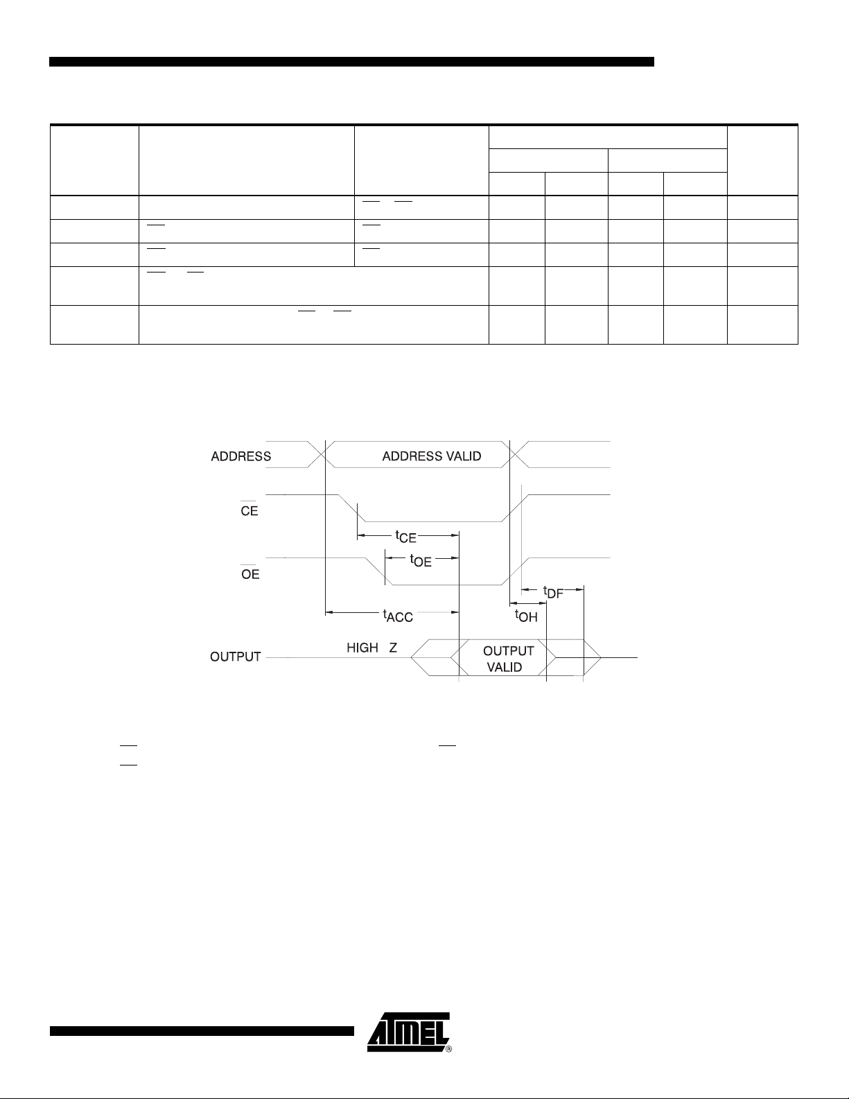
9. AC Characteristics for Read Operation
Symbol Parameter Condition
(1)
t
ACC
(1)
t
CE
(1)
t
OE
(1)
t
DF
t
OH
Note: 1. See AC Waveforms for Read Operation.
Address to Output Delay CE = OE = V
CE to Output Delay OE = V
OE to Output Delay CE = V
IL
IL
OE or CE High to Output
Float, Whichever Occurred First
Output Hold from Address, CE or OE,
Whichever Occurred First
AT27C256R
AT27C256R
-45 -70
Min Max Min Max
IL
45 70 ns
45 70 ns
20 30 ns
20 25 ns
77 ns
Units
10. AC Waveforms for Read Operation
(1)
Notes: 1. Timing measurement reference level is 1.5V for -45 devices. Input AC drive levels are VIL = 0.0V and VIH = 3.0V. Timing mea-
surement reference levels for all other speed grades are V
and V
2. OE
3. OE
= 2.4V.
IH
may be delayed up to tCE - tOE after the falling edge of CE without impact on tCE.
may be delayed up to t
- tOE after the address is valid without impact on t
ACC
= 0.8V and VOH = 2.0V. Input AC drive levels are VIL = 0.45V
OL
.
ACC
4. This parameter is only sampled and is not 100% tested.
5. Output float is defined as the point when data is no longer driven.
0014K–EPROM–10/05
5
Page 6

11. Input Test Waveforms and Measurement Levels
For -45 devices only:
t
, tF < 5 ns (10% to 90%)
R
For -70 devices:
tR, tF < 20 ns (10% to 90%)
12. Output Test Load
Note: 1. CL = 100 pF including jig capacitance, except for the -45 devices, where CL = 30 pF.
13. Pin Capacitance
f = 1 MHz, T = 25°C
Symbol Typ Max Units Conditions
C
IN
C
OUT
Note: 1. Typical values for nominal supply voltage. This parameter is only sampled and is not 100% tested.
(1)
46pFV
812pFV
IN
OUT
= 0V
= 0V
6
AT27C256R
0014K–EPROM–10/05
Page 7

AT27C256R
14. Programming Waveforms
(1)
Notes: 1. The Input Timing Reference is 0.8V for VIL and 2.0V for VIH.
2. tOE and t
are characteristics of the device but must be accommodated by the programmer.
DFP
3. When programming the AT27C256R a 0.1 µF capacitor is required across VPP and ground to suppress spurious voltage
transients.
15. DC Programming Characteristics
TA = 25 ± 5°C, VCC = 6.5 ± 0.25V, VPP = 13.0 ± 0.25V
Symbol Parameter Test Conditions
I
V
V
V
V
I
I
V
LI
IL
IH
OL
OH
CC2
PP2
ID
Input Load Current V
= VIL,V
IN
IH
Input Low Level -0.6 0.8 V
Input High Level 2.0 VCC + 1 V
Output Low Volt IOL = 2.1 mA 0.4 V
Output High Volt I
= -400 µA 2.4 V
OH
VCC Supply Current (Program and Verify) 25 mA
VPP Current CE = V
IL
A9 Product Identification Voltage 11.5 12.5 V
Limits
UnitsMin Max
±10 µA
25 mA
0014K–EPROM–10/05
7
Page 8

16. AC Programming Characteristics
TA = 25 ± 5°C, VCC = 6.5 ± 0.25V, VPP = 13.0 ± 0.25V
Symbol Parameter Test Conditions
Limits
(1)
UnitsMin Max
t
t
t
t
t
t
t
t
t
t
t
AS
OES
DS
AH
DH
DFP
VPS
VCS
PW
OE
PRT
Address Setup Time
OE Setup Time 2 µs
Data Setup Time 2 µs
Input Rise and Fall Times
(10% to 90%) 20 ns
Address Hold Time 0 µs
Input Pulse Levels
Data Hold Time 2 µs
OE High to Output Float Delay
VPP Setup Time 2 µs
(2)
Input Timing Reference Level
0.45V to 2.4V
0.8V to 2.0V
VCC Setup Time 2 µs
CE Program Pulse Width
Data Valid from OE
(3)
(2)
Output Timing Reference Level
0.8V to 2.0V
VPP Pulse Rise Time During Programming 50 ns
Notes: 1. VCC must be applied simultaneously or before VPP and removed simultaneously or after VPP.
2. This parameter is only sampled and is not 100% tested. Output Float is defined as the point where data is no longer
driven – see timing diagram.
3. Program Pulse width tolerance is 100
µsec ± 5%.
17. Atmel’s AT27C256R Integrated Product Identification Code
Pins
Codes
2µs
0 130 ns
95 105 µs
150 ns
Hex
DataA0 O7 O6 O5 O4 O3 O2 O1 O0
Manufacturer 000011110 1E
Device Type 110001100 8C
8
AT27C256R
0014K–EPROM–10/05
Page 9

18. Rapid Programming Algorithm
A 100 µs CE pulse width is used to program. The address is set to the first location. VCC is
raised to 6.5V and V
CE
pulse without verification. Then a verification/reprogramming loop is executed for each
address. In the event a byte fails to pass verification, up to 10 successive 100 µs pulses are
applied with a verification after each pulse. If the byte fails to verify after 10 pulses have been
applied, the part is considered failed. After the byte verifies properly, the next address is
selected until all have been checked. V
are read again and compared with the original data to determine if the device passes or fails.
PP
AT27C256R
is raised to 13.0V. Each address is first programmed with one 100 µs
is then lowered to 5.0V and VCC to 5.0V. All bytes
PP
0014K–EPROM–10/05
9
Page 10

19. Ordering Information
19.1 Standard Package
I
t
ACC
(ns)
45 20 0.1 AT27C256R-45JI
70 20 0.1 AT27C256R-70JI
Note: Refer to PCN# SC042702.
19.2 Green Package (Pb/Halide-free)
t
ACC
(ns)
45 20 0.1 AT27C256R-45JU
70 20 0.1 AT27C256R-70JU
(mA)
CC
Ordering Code Package Operation RangeActive Standby
AT27C256R-45PI
AT27C256R-45RI
AT27C256R-45TI
AT27C256R-70PI
AT27C256R-70RI
AT27C256R-70TI
20 0.1 AT27C256R-70JA
AT27C256R-70PA
AT27C256R-70RA
I
(mA)
CC
Ordering Code Package Operation RangeActive Standby
AT27C256R-45PU
AT27C256R-45RU
AT27C256R-45TU
AT27C256R-70PU
AT27C256R-70RU
AT27C256R-70TU
32J
28P6
28R
28T
32J
28P6
28R
28T
32J
28P6
28R
32J
28P6
28R
28T
32J
28P6
28R
28T
Industrial
(-40°C to 85°C)
Industrial
(-40°C to 85°C)
Automotive
(-40°C to 125°C)
Industrial
(-40°C to 85°C)
Industrial
(-40°C to 85°C)
Package Type
32J 32-lead, Plastic J-Leaded Chip Carrier (PLCC)
28P6 28-lead, 0.600" Wide, Plastic Dual Inline Package (PDIP)
28R 28-lead, 0.330" Wide, Plastic Gull Wing Small Outline (SOIC)
28T 28-lead, Thin Small Outline Package (TSOP)
10
AT27C256R
0014K–EPROM–10/05
Page 11

20. Packaging Information
20.1 32J – PLCC
AT27C256R
1.14(0.045) X 45˚
B
e
0.51(0.020)MAX
45˚ MAX (3X)
Notes: 1. This package conforms to JEDEC reference MS-016, Variation AE.
2. Dimensions D1 and E1 do not include mold protrusion.
Allowable protrusion is .010"(0.254 mm) per side. Dimension D1
and E1 include mold mismatch and are measured at the extreme
material condition at the upper or lower parting line.
3. Lead coplanarity is 0.004" (0.102 mm) maximum.
PIN NO. 1
IDENTIFIER
D1
D
D2
1.14(0.045) X 45˚
E1 E
0.318(0.0125)
0.191(0.0075)
E2
B1
A2
A1
A
COMMON DIMENSIONS
(Unit of Measure = mm)
SYMBOL
A 3.175 – 3.556
A1 1.524 – 2.413
A2 0.381 – –
D 12.319 – 12.573
D1 11.354 – 11.506 Note 2
D2 9.906 – 10.922
E 14.859 – 15.113
E1 13.894 – 14.046 Note 2
E2 12.471 – 13.487
B 0.660 – 0.813
B1 0.330 – 0.533
e 1.270 TYP
MIN
NOM
MAX
NOTE
10/04/01
2325 Orchard Parkway
R
San Jose, CA 95131
0014K–EPROM–10/05
TITLE
32J, 32-lead, Plastic J-leaded Chip Carrier (PLCC)
DRAWING NO.
32J
REV.
B
11
Page 12

20.2 28P6 – PDIP
PIN
1
E1
A1
B
REF
E
B1
C
L
SEATING PLANE
A
e
D
0º ~ 15º
eB
Notes: 1. This package conforms to JEDEC reference MS-011, Variation AB.
2. Dimensions D and E1 do not include mold Flash or Protrusion.
Mold Flash or Protrusion shall not exceed 0.25 mm (0.010").
TITLE
2325 Orchard Parkway
R
San Jose, CA 95131
28P6, 28-lead (0.600"/15.24 mm Wide) Plastic Dual
Inline Package (PDIP)
COMMON DIMENSIONS
(Unit of Measure = mm)
SYMBOL
A – – 4.826
A1 0.381 – –
D 36.703 – 37.338 Note 2
E 15.240 – 15.875
E1 13.462 – 13.970 Note 2
B 0.356 – 0.559
B1 1.041 – 1.651
L 3.048 – 3.556
C 0.203 – 0.381
eB 15.494 – 17.526
e 2.540 TYP
MIN
NOM
MAX
DRAWING NO.
28P6
NOTE
09/28/01
REV.
B
12
AT27C256R
0014K–EPROM–10/05
Page 13

20.3 28R – SOIC
AT27C256R
B
E
1
PIN 1
e
D
A
1
0º ~ 8º
C
L
Note: 1. Dimensions D and E1 do not include mold Flash
or protrusion. Mold Flash or protrusion shall not exceed
0.25 mm (0.010").
E
A
COMMON DIMENSIONS
(Unit of Measure = mm)
SYMBOL
A 2.39 – 2.79
A1 0.050 – 0.356
D 18.00 – 18.50 Note 1
E 11.70 – 12.50
E 1 8.59 – 8.79 Note 1
B 0.356 – 0.508
C 0.203 – 0.305
L 0.94 – 1.27
e 1.27 TYP
MIN
NOM
MAX
NOTE
2325 Orchard Parkway
R
San Jose, CA 95131
0014K–EPROM–10/05
TITLE
28R, 28-lead, 0.330" Body Width,
Plastic Gull Wing Small Outline (SOIC)
5/18/2004
DRAWING NO.
28R
REV.
C
13
Page 14

20.4 28T – TSOP
PIN 1
Pin 1 Identifier Area
D1
D
e
E
b
A2
A
A1
Notes: 1. This package conforms to JEDEC reference MO-183.
2. Dimensions D1 and E do not include mold protrusion. Allowable
protrusion on E is 0.15 mm per side and on D1 is 0.25 mm per side.
3. Lead coplanarity is 0.10 mm maximum.
0º ~ 5º
SEATING PLANE
SYMBOL
c
L
L1
GAGE PLANE
COMMON DIMENSIONS
(Unit of Measure = mm)
MIN
A – – 1.20
A1 0.05 – 0.15
A2 0.90 1.00 1.05
D 13.20 13.40 13.60
D1 11.70 11.80 11.90 Note 2
E 7.90 8.00 8.10 Note 2
L 0.50 0.60 0.70
L1 0.25 BASIC
b 0.17 0.22 0.27
c 0.10 – 0.21
e 0.55 BASIC
NOM
MAX
NOTE
14
2325 Orchard Parkway
R
San Jose, CA 95131
AT27C256R
TITLE
28T, 28-lead (8 x 13.4 mm) Plastic Thin Small Outline
Package, Type I (TSOP)
DRAWING NO.
28T
0014K–EPROM–10/05
12/06/02
REV.
C
Page 15

Atmel Corporation Atmel Operations
2325 Orchard Parkway
San Jose, CA 95131, USA
Tel: 1(408) 441-0311
Fax: 1(408) 487-2600
Regional Headquarters
Europe
Atmel Sarl
Route des Arsenaux 41
Case Postale 80
CH-1705 Fribourg
Switzerland
Tel: (41) 26-426-5555
Fax: (41) 26-426-5500
Asia
Room 1219
Chinachem Golden Plaza
77 Mody Road Tsimshatsui
East Kowloon
Hong Kong
Tel: (852) 2721-9778
Fax: (852) 2722-1369
Japan
9F, Tonetsu Shinkawa Bldg.
1-24-8 Shinkawa
Chuo-ku, Tokyo 104-0033
Japan
Tel: (81) 3-3523-3551
Fax: (81) 3-3523-7581
Memory
2325 Orchard Parkway
San Jose, CA 95131, USA
Tel: 1(408) 441-0311
Fax: 1(408) 436-4314
Microcontrollers
2325 Orchard Parkway
San Jose, CA 95131, USA
Tel: 1(408) 441-0311
Fax: 1(408) 436-4314
La Chantrerie
BP 70602
44306 Nantes Cedex 3, France
Tel: (33) 2-40-18-18-18
Fax: (33) 2-40-18-19-60
ASIC/ASSP/Smart Cards
Zone Industrielle
13106 Rousset Cedex, France
Tel: (33) 4-42-53-60-00
Fax: (33) 4-42-53-60-01
1150 East Cheyenne Mtn. Blvd.
Colorado Springs, CO 80906, USA
Tel: 1(719) 576-3300
Fax: 1(719) 540-1759
Scottish Enterprise Technology Park
Maxwell Building
East Kilbride G75 0QR, Scotland
Tel: (44) 1355-803-000
Fax: (44) 1355-242-743
RF/Automotive
Theresienstrasse 2
Postfach 3535
74025 Heilbronn, Germany
Tel: (49) 71-31-67-0
Fax: (49) 71-31-67-2340
1150 East Cheyenne Mtn. Blvd.
Colorado Springs, CO 80906, USA
Tel: 1(719) 576-3300
Fax: 1(719) 540-1759
Biometrics/Imaging/Hi-Rel MPU/
High Speed Converters/RF Datacom
Avenue de Rochepleine
BP 123
38521 Saint-Egreve Cedex, France
Tel: (33) 4-76-58-30-00
Fax: (33) 4-76-58-34-80
Literature Requests
www.atmel.com/literature
Disclaimer: The information in this document is provided in connection with Atmel products. No license, express or implied, by estoppel or otherwise, to any
intellectual property right is granted by this document or in connection with the sale of Atmel products. EXCEPT AS SET FORTH IN ATMEL’S TERMS AND CONDI-
TIONS OF SALE LOCATED ON ATMEL’S WEB SITE, ATMEL ASSUMES NO LIABILITY WHATSOEVER AND DISCLAIMS ANY EXPRESS, IMPLIED OR STATUTORY
WARRANTY RELATING TO ITS PRODUCTS INCLUDING, BUT NOT LIMITED TO, THE IMPLIED WARRANTY OF MERCHANTABILITY, FITNESS FOR A PARTICULAR
PURPOSE, OR NON-INFRINGEMENT. IN NO EVENT SHALL ATMEL BE LIABLE FOR ANY DIRECT, INDIRECT, CONSEQUENTIAL, PUNITIVE, SPECIAL OR INCIDENTAL DAMAGES (INCLUDING, WITHOUT LIMITATION, DAMAGES FOR LOSS OF PROFITS, BUSINESS INTERRUPTION, OR LOSS OF INFORMATION) ARISING OUT
OF THE USE OR INABILITY TO USE THIS DOCUMENT, EVEN IF ATMEL HAS BEEN ADVISED OF THE POSSIBILITY OF SUCH DAMAGES. Atmel makes no
representations or warranties with respect to the accuracy or completeness of the contents of this document and reserves the right to make changes to specifications
and product descriptions at any time without notice. Atmel does not make any commitment to update the information contained herein. Unless specifically provided
otherwise, Atmel products are not suitable for, and shall not be used in, automotive applications. Atmel’s products are not intended, authorized, or warranted for use
as components in applications intended to support or sustain life.
© Atmel Corporation 2005. All rights reserved. Atmel®, logo and combinations thereof, Everywhere You Are® and others, are
registered trademarks or trademarks of Atmel Corporation or its subsidiaries. Other terms and product names may be trademarks of others.
Printed on recycled paper.
0014K–EPROM–10/05
 Loading...