

Datasheet AT27BV800-15JI, AT27BV800-15JC, AT27BV800-12TI, AT27BV800-12TC, AT27BV800-12RI Datasheet (ATMEL)
...Page 1
Features
•
Read Access Time - 120 ns
•
Word-wide or Byte-wide Configurable
•
Dual Voltage Range Operation
– Unregulated Battery Power Supply Range, 2.7V to 3.6V
or Standard 5V
•
8-Megabit Flash and Mask ROM Compatable
•
Low Power CMOS Operation
µ
–20
A Maximum Standby
– 10 mA Max. Active at 5 MHz for V
•
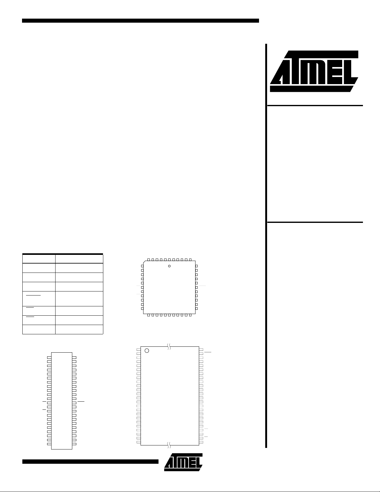
JEDEC Standard Packages
– 44-Lead PLCC
– 44-Lead SOIC (SOP)
– 48-Lead TSOP (12 mm x 20 mm)
•
High Reliability CMOS Technology
– 2,000 ESD Protection
– 200 mA Latchup Immunity
•
Rapid™ Programming Algorithm - 50
•
CMOS and TTL Compatible Inputs and Outputs
– JEDEC Standard for LVTTL and LVBO
•
Integrated Product Identification Code
•
Commercial and Industrial Temperature Ranges
±±±±
10% Supply Range
= 3.6V
CC
µ
s/word (typical)
8-Megabit
(512K x 16 or
1024K x 8)
Unregulated
Battery-Voltage
High Speed
™
Description
The AT27BV800 is a high performance low-power, low-voltage 8,388,608-bit one time
programmable read only memory (OTP EPROM) organized as either 512K by 16 or
1024K by 8 bits. It r eq uire s o nl y one su ppl y in the r ang e of 2.7 to 3.6V i n n ormal r ea d
Pin Configurations
Pin Name Function
A0 - A18 Addresses
O0 - O15 Outputs
O15/A-1 Output/Address
Byte Mode/
/V
BYTE
CE
OE
NC No Connect
PP
Program Supply
Chip Enable
Output En able
SOIC (SOP)
1
NC
2
A18
3
A17
4
A7
5
A6
6
A5
7
A4
8
A3
9
A2
10
A1
11
A0
12
CE
13
GND
14
OE
15
O0
16
O8
17
O1
18
O9
19
O2
20
O10
21
O3
22
O11
44
NC
43
NC
42
A8
41
A9
40
A10
39
A11
38
A12
37
A13
36
A14
35
A15
34
A16
33
BYTE/VPP
32
GND
31
O15/A-1
30
O7
29
O14
28
O6
27
O13
26
O5
25
O12
24
O4
23
VCC
A15
A14
A13
A12
A11
A10
A18
A17
A5A6A7
65432
7
A4
8
A3
9
A2
10
A1
11
A0
12
CE
13
GND
14
OE
15
O0
16
O8
17
O1
1819202122232425262728
O9
1
2
3
4
5
6
7
A9
8
A8
9
NC
10
NC
11
NC
12
NC
13
NC
14
NC
15
NC
16
17
18
A7
19
A6
20
A5
21
A4
22
A3
23
A2
24
A1
O2
O16O3O11
TSOP
Type 1
PLCC
A17
A18
GNDNCA8A9A10
1
NC
4443424140
O4
O12O5O13
VCC
A11
39
38
37
36
35
34
33
32
31
30
29
A12
A13
A14
A15
A16
BYTE/VPP
GND
O15/A-1
O7
O14
O6
48
47
46
45
44
43
42
41
40
39
38
37
36
35
34
33
32
31
30
29
28
27
26
25
A16
BYTE/VPP
GND
O15/A-1
O7
O14
O6
O13
O5
O12
O4
VCC
O11
O3
O10
O2
O9
O1
O8
O0
OE
GND
CE
A0
(continued)
OTP EPROM
AT27BV800
Preliminary
AT27BV800
Preliminary
Rev. 0988B–03/98
1
Page 2
mode operation. The x16 organization makes this part ideal
for portable and hand held 16- and 32-bit microp rocessor
based systems using either regulated or unregulate d battery power.
Atmel’s innovative design te chniques provide f ast speeds
that rival 5V parts while ke eping the low power c onsumption of a 3V supply. At V
= 2.7V, any w ord can be
CC
accessed in less than 120ns. With a typical power dissipation of only 10 mW at 5mHZ and V
= 3V, the AT27BV800
CC
consumes less than one fifth the power of a standard 5V
EPROM.
Standby mode supply cu rrent is typica lly less than 1 mA at
3V. The AT27BV800 simplifies system design an d
stretches battery lifetime e ven furthe r by elim inating th e
need for power supply regulation.
The AT27BV800 can be organized as either word-wide or
byte-wide. The org anizatio n is se lected v ia the B YTE
/V
PP
pin. When BYTE/VPP is asserted high (VIH), the word-wide
organization is sele cted and the O15/A-1 pi n is used for
O15 data output. When BY TE
/VPP is asserted low (VIL),the
byte wide organization is se lected and the O 15/A-1 pin is
used for the address pin A-1. When the AT27BV800 is logically regarded as x16 (word-wide), but read in the bytewide mode, then with A-1=V
bit word are selected with A-1 =V
the lower eight bits of the 16
IL
the upper 8 bits of the
IH
16-bit word are selected.
The AT27BV800 is available in industry standard JEDEC-
approved one-time programmable (OTP) PLCC, SOIC
(SOP), and TSOP packages. The device features two-line
control(CE
,OE) to elimi nate bu s cont ention in h igh-spee d
systems.
With high den sity 51 2K word o r 1 024K -bit stor age capa bil-
ity, the AT27B V800 allo ws fir mware to be to b e sto red reliably and to be accessed by the system without the delays
of mass storage media.
The AT27BV800 op eratin g with V
at 3.0V produces TTL
CC
level outputs that are compatible with standard TTL logic
devices operating at V
= 5V. At VCC = 2.7V, the part is
CC
compatible with JEDEC approved low voltage battery operation (LVBO) interface specifications. T he device is als o
capable of standard 5-volt operation making it ideally suited
for dual sup ply rang e system s or card produc ts that are
pluggable in both 3-volt and 5-volt hosts.
Atmel’s AT27BV800 has additional features that ensure
high quality a nd e ffici ent produc tion use . The Rapi d
TM
Programming Algorithm reduces the time required to program
the part and guarantees reliable programming. Programming time is typical ly on ly 50µ s/word. The In tegrated Product Identification Code electronically identifies the device
and manufacturer. This feature is used by industry standard
programming equi pmen t to se lect the prop er progr amm ing
equipment and voltages. The AT27BV800 programs
exactly the same way as a standard 5V AT27C800 and
uses the same programming equipment.
System Considerations
Switching between active and standby conditions via the
Chip Enable pin may produce trans ient voltage excursions.
Unless accommodated by the system design, these transients may exceed data sheet limits, resulting in device
non-conforman ce. At a mini mum, a 0.1 µF high freque ncy,
low inherent induc tance, cera mic capacitor should be utilized for each device. This capacitor should be connected
between the V
close to the device as possible. Additionally, to stabilize the
supply voltage level on printed circuit boards with large
EPROM arra ys, a 4.7 µ F bulk electrolytic capacitor should
be utilized, again connected between the V
terminals. This capacitor should be positioned as close as
possible to the point where the power supply is connected
to the array.
and Ground terminals of the device, as
CC
and Ground
CC
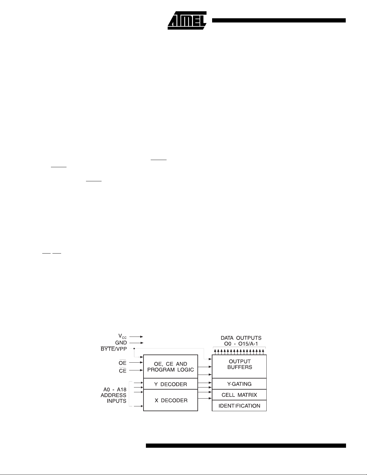
Block Diagram
2
AT27BV800
Page 3
Absolute Maximum Ratings*
AT27BV800
Temperature Under Bias................................ -55°C to +125°C
*NOTICE: Stresses beyond those listed under “Absolute
Maximum Ratings” may cause permanent dam-
Storage Temperature..................................... -65°C to +150°C
age to the device. This i s a stress rating only a nd
functional operation of the device at these or any
Voltage on Any Pin with
with Respect to Ground..................................-2.0V to +7.0V
(1)
other conditions beyond those indicated in the
operational sections of this specification is not
implied. Exposure to absolute maximum rating
Voltage on A9 with
Respect to Ground ......................................-2.0V to +14.0V
(1)
conditions f or e xtended p eriods ma y aff ect de vice
reliability.
Note: 1. Minimum voltage is -0.6V DC which may under-
VPP Supply Voltage with
Respect to Ground .......................................-2.0V to +14.0V
(1)
shoot to -2.0V for pulses of less than 20 ns. Max-
imum output pin voltage is Vcc + 0.75V DC which
may overshoot to + 7.0V for pulses of less than
20 ns.
Operating Modes
Mode/Pin CE OE Ai BYTE/V
Read Word-wide V
Read Byte-wide Upper V
Read Byte-wide Lower V
Output Disable X
Standby V
Rapid Program
(3)
IL
IL
IL
(1)
IH
V
IL
PGM Verify X V
PGM Inhibit V
Product Identi fi cation
Notes: 1. X can be VIL or V
(5)
IH.
IH
V
IL
2. Read, output disable, and stand by modes require, 2.7V ≤ VCC ≤ 3.6V, or 4.5V ≤ VCC ≤ 5.5V.
3. Refer to the programming characteristics tables in this data sheet.
= 12.0 ± 0.5V.
4. V
H
5. Two identifier words may be selected. All Ai inputs are held low (VIL) except A9,which is set to VH, and A0, which is toggled
low (V
) to select the Manufacturer’s Identification word and high (VIH) to select the Device Code word.
IL
6. Standby VCC current (ISB) is specified with VPP = VCC. VCC > VPP will cause a slight increase in I
V
IL
V
IL
V
IL
V
IH
(1)
X
V
IH
IL
V
IH
V
IL
(1)
X
(1)
X
(1)
X
(1)
X
(1)
X
Ai V
Ai V
(1)
X
(4)
A9 = V
H
A0 = VIH or V
A1 - A18 = V
IL
IL
Outputs
O
PP
V
IH
V
IL
V
IL
0-O7
D
OUT
D
OUT
D
OUT
X High Z
(6)
X
PP
PP
V
PP
V
IH
SB.
O8-O
D
High Z V
High Z V
High Z
D
D
High Z
Identification Code
OUT
IN
OUT
14
O15/A-1
D
OUT
IH
IL
3
Page 4
DC and AC Operating Conditions for Read Operation
Operating Temperature (Case)
V
Power Supply
CC
Com. 0°C - 70°C0
Ind.
AT27BV800
-12 -15
°
C - 70°C
-40°C - 85°C-40
2.7V to 3.6V 2.7V to 3.6V
5V ± 10% 5V ± 10%
°
C - 85°C
DC and Operating Characteristics for Read Operation
= Preliminary
Symbol Parameter Condition Min Max Units
VCC = 2.7V to 3.6V
±
I
LI
I
LO
(2)
I
PP1
I
SB
I
CC
V
IL
V
IH
V
OL
V
OH
Input Load Current VIN = 0V to V
Output Leakage Current V
(1)
V
Read/Standby Current V
PP
(1)
V
Standby Current
CC
= 0V to V
OUT
= V
PP
CC
(CMOS), CE = V
I
SB1
I
(TTL), CE = 2.0 to V
SB2
VCC Active Current f = 5MHz, I
= 3.0 to 3.6V -0.6 0.8 V
V
Input Low Voltage
Input High Voltage
Output Low Voltage
Output High Voltage
CC
V
= 2.7 to 3.6V -0.6 0.2 x V
CC
= 3.0 to 3.6V 2.0 VCC + 0.5 V
V
CC
V
= 2.7 to 3.6V 0.7 x V
CC
= 2.0 mA 0.4 V
I
OL
I
= 100 µA0.2V
OL
I
= 20 µA0.1V
OL
= -2.0 mA 2.4 V
I
OH
I
= -100 µAV
OH
I
= -20 µAV
OH
CC
CC
±
0.3V 20
CC
+ 0.5V 100 mA
CC
= 0 mA, CE = VIL, VCC = 3.6V 10 mA
OUT
CC
- 0.2 V
CC
- 0.1 V
CC
VCC = 4.5V to 5.5V
I
I
I
I
I
V
V
V
V
LI
LO
PP1
SB
CC
(2)
IL
IH
OL
OH
Input Load Current VIN = 0V to V
Output Leakage Current V
(1)
V
Read/Standby Current V
PP
(1)
V
Standby Current
CC
OUT
= V
PP
(CMOS), CE = V
I
SB1
I
(TTL), CE = 2.0 to V
SB2
VCC Active Current f = 5MHz, I
= 0V to V
CC
OUT
CC
CC
±
0.3V 100
CC
CC
= 0 mA, CE = V
+ 0.5V 1 mA
IL
Input Low Voltage -0.6 0.8 V
Input High Voltage 2.0 VCC + 0.5 V
Output Low Voltage IOH = -2.1 mA 0.4 V
Output High Voltage I
= -400 µA2.4V
OH
Notes: 1. VCC must be applied simultaneously or before VPP, and removed simultaneously or after VPP.
2. VPP may be connected directly to VCC except during programming. The supply current would then be the sum of I
1
±
5
10
CC
VCC + 0.5 V
±
1.0
±
5.0
10
40 mA
CC
µ
A
µ
A
µ
A
µ
A
V
µ
A
µ
A
µ
A
µ
A
and IPP.
4
AT27BV800
Page 5

AC Characteristics for Read Operation
(VCC = 2.7V to 3.6V and 4.5V to 5.5V)
AT27BV800
AT27BV800
-12 -15
Symbol Parameter Condition
t
ACC
t
CE
t
OE
t
DF
t
OH
t
ST
t
STD
(3)
(2)
(2,3)
(4,5)
(4)
Address to Output Delay CE = OE = V
CE to Output Delay OE = V
OE to Output Delay CE = V
OE or CE High to Output Float, whichever
occured first
Output Hold from Address CE or OE,
whichever occured first
BYTE High to Output Valid 120 150 ns
BYTE Low to Output Transition 50 60 ns
Notes: 2,3,4,5. See the AC Waveforms for Read Operation diagram.
Byte-Wide Read Mode AC Waveforms
(1)
Min Max Min Max
IL
IL
IL
120 150 ns
120 150 ns
40 50 ns
Units
35 40 ns
5.0 5.0 ns
= Preliminary
Note: 1. BYTE/VPP = V
IL
Word-Wide Read Mode AC Waveforms
Note: 1. BYTE/VPP = V
IH
(1)
5
Page 6

BYTE
Transition AC Waveforms
A0-A18
A-1
t
BYTE/V
PP
O-O
07
t
OH
O-O
815
t
STD
Notes: 1. Timing measurement references are 0.8V and 2.0V. Input AC drive levels are 0.45V and 2.4V, unless otherwise specified.
2. OE may be delayed up to tCE - tOE after the falling edge of CE without impact on t
3. OE may be delayed up to t
4. This parameter is only sampled and is not 100% tested.
5. Output float is defined as the point when data is no longer driven.
- tOE after the address is valid without impact on t
ACC
ACC
VALID
VALID
DATAOUT
HI-Z
t
OH
t
ST
DATAOUT
DATAOUT
CE.
.
ACC
Input Test Waveforms and Measurement Levels
tR, tF < 20 ns (10% to 90%)
Output Test Load
Note: CL = 100 pF including jig
capacitance.
Pin Capaticance
(f = 1 MHz, T = 25°C)
C
IN
C
OUT
Note: 1. Typical values for nominal supply voltage. This parameter is only sampled and is not 100% tested.
6
(1)
Typ Max Units Conditions
410pFV
812pFV
AT27BV800
IN
OUT
= 0V
= 0V
Page 7

AT27BV800
Programming Waveforms
(1)
Notes: 1. The Input Timing reference is 0.8V for VIL and 2.0V for VIH.
and t
2. t
OE
3. When programming the AT27BV800, a 0.1 µF capacitor is required across VPP and ground to suppress voltage transients.
are characteristics of the device but must be accommodated by the programmer.
DFP
DC Programming Characteristics
TA = 25 ± 5°C, VCC = 6.5 ± 0.25V, VPP = 13.0 ± 0.25V
Symbol Parameter Test Conditions
I
LI
V
IL
V
IH
V
OL
V
OH
I
CC2
I
PP2
V
ID
Input Load Current VIN = VIL, V
Input Low Level -0.6 0.8 V
Input High Level 2.0 V
Output Low Voltage IOL = 2.1 mA 0.4 V
Output High Voltage IOH = -400 µA2.4 V
VCC Supply Current (Program and Verify) 50 mA
VPP Supply Current CE = V
A9 Product Identification Voltage 11.5 12.5 V
IH
IL
Limits
10
±
+ 0.5 V
CC
30 mA
UnitsMin Max
A
µ
7
Page 8

AC Programming Characteristics
TA = 25 ± 5°C, VCC = 6.5 ± 0.25V, VPP = 13.0 ± 0.25V
Symbol Parameter Test Conditions
(1)
Limits
UnitsMin Max
t
AS
t
OES
t
DS
t
AH
t
DH
t
DFP
t
VPS
t
VCS
t
PW
t
OE
t
PRT
Address Setup Time
OE Setup Time 2
Input Rise and Fall Times:
(10% to 90%) 20 ns.
Data Setup Time 2
Address Hold Time 0
Input Pulse Levels:
0.45V to 2.4V
Data Hold Time 2
OE High to Output Float Delay
(2)
VPP Setup Time 2
VCC Setup Time 2
CE Program Pulse Width
(3)
Data Valid from OE 150 ns
BYTE /VPP Pulse Rise T ime During
Input Pulse Levels:
0.8V to 2.0V
Input Timing Reference Level:
0.8V to 2.0V
Output Timing Reference Level:
0.8V to 2.0V
Programming
Notes: 1. V
must be applied simultaneously or before V
cc
2. This para meter is on ly sampled a nd is not 10 0% tested . Output Flo at is defin ed as the po int where data is no l onger driv en—
see timing diagram.
3. Program Pulse width tolerance is 50 µs ± 5%.
and removed simultaneously or after VPP.
PP
Atmel’s 27BV800 Integrated Product Identification Code
2
0 130 ns
47.5 52.5
50 ns
(1)
s
µ
s
µ
s
µ
s
µ
s
µ
s
µ
s
µ
s
µ
Pins
A0 O15 O14 O13 O12 O11 O10 O9 O8
Codes
O7 O6 O5 O4 O3 O2 O1 O0
Hex Data
Manufacturer 000011110 1E1E
Device Type 111111000 F8F8
Note: 1. The AT27BV800 has the same Product Identification Code as the AT27C800. Both are programming compatible.
8
AT27BV800
Page 9

Rapid Programming Algorithm
A 50 µs CE pulse width is used to pr og r am. The addres s is
set to the first location. V
is raised to 13.0V. Each add ress is fir st programmed with
one 50 µs CE
tion/reprogramming loo p is exec uted for each addres s. In
the event a word fails to pass verificati on, up to 1 0 succ essive 50 µs pulses are applied with a verification after each
pulse without verification. Then a verifica-
is raised to 6.5V and BYTE/V
CC
PP
AT27BV800
pulse. If the word fails to verify after 10 pulses have been
applied, the part is considered failed. After the word verifies
properly, the next address is selected until all have been
checked. V
words are read again and compared with the original data
to determine if the device passes or fails.
is then lowered to 5.0V and VCC to 5.0V. All
PP
9
Page 10

Ordering Information
t
ACC
(ns)
120 10 0.02 AT27BV800-12JC
150 10 0.02 AT27BV800-15JC
ICC (mA)
Ordering Code Package Operation RangeActive Standby
AT27BV800-12RC
AT27BV800-12TC
10 0.02 AT27BV800-12JI
AT27BV800-12RI
AT27BV800-12TI
AT27BV800-15RC
AT27BV800-15TC
10 0.02 AT27BV800-15JI
AT27BV800-15RI
AT27BV800-15TI
44J
44R
48T
44J
44R
48T
44J
44R
48T
44J
44R
48T
Commercial
(0°C to 70°C)
Industrial
(-40°C to 85°C)
Commercial
(0°C to 70°C)
Industrial
(-40°C to 85°C)
= Preliminary
10
44J
44R
48T
Package Type
44-Lead, Plastic J-Leaded Chip Carrier (PLCC)
44-Lead, 0.525" Wide, Plastic Gull Wing Small Outline Package (SOIC/SOP)
48-Lead, Plastic Thin Small Outline Package (TSOP) 12 x 20 mm
AT27BV800
Page 11

Packaging Information
44-Lead, 0.525" Wide,
44R,
Plastic Gull Wing Small Outline Package (SOIC/SOP)
Dimensions in Inches and (Millimeters)
AT27BV800
48-Lead, 12 x 20 mm,
48T,
Plastic Thin Small Outline Package(TSOP)
Dimensions in Millimeters and (Inches)*
JEDEC OUTLINE MO-142 BD
44J
, 44-Lead, Plastic J-Leaded Chip Carrier (PLCC)
Dimensions in Inches and (Millimeters)
JEDEC STANDARD MS-018 AC
.045(1.14) X 45°
.032(.813)
.026(.660)
.050(1.27) TYP
PIN NO.1
IDENTIFY
.500(12.7) REF SQ
.045(1.14) X 30° - 45°
.656(16.7)
SQ
.650(16.5)
.695(17.7)
SQ
.685(17.4)
.022(.559) X 45° MAX (3X)
.012(.305)
.008(.203)
.630(16.0)
.590(15.0)
.021(.533)
.013(.330)
.043(1.09)
.020(.508)
.120(3.05)
.090(2.29)
.180(4.57)
.165(4.19)
*Controlling dimension: millimeters
11
 Loading...