

Datasheet AT25256W-10SI-2.7, AT25256W-10SI-1.8, AT25256W-10SI, AT25256W-10SC-2.7, AT25256W-10SC-1.8 Datasheet (ATMEL)
...Page 1
Features
Serial Peripheral Interface (SPI) Compatible
•
Supports SPI Modes 0 (0,0) and 3 (1,1)
•
Low Voltage and Standard Voltage Operation
•
– 5.0 (VCC = 4.5V to 5.5V)
– 2.7 (VCC = 2.7V to 5.5V)
– 1.8 (VCC = 1.8V to 3.6V)
3 MHz Clock Rate
•
64-Byte Page Mode and Byte Write Operation
•
Block Write Protection
•
– Protect 1/4, 1/2, or Entire Array
Write Protect (WP) Pin and Write Disable Instructions for
•
Both Hardware and Software Data Protection
Self-Timed Write Cycle (5 ms Typical)
•
High Reliability
•
– Endurance: 100,000 Write Cycles
– Data Retention: >200 Years
– ESD Protection: >4000V
Automotive Grade and Extended Temperature Devices Available
•
8-Pin PDIP, 8-Pin EIAJ SOIC, 8-Pin and 16-Pin JEDEC SOIC, 14-Pin and 20-Pin TSSOP,
•
and 8-Pin Leadless Array Packages
Description
The AT25128/256 provides 131,072 /262,144 bits of s erial el ectrical ly eras able programmable read only memory (EEPROM) organized as 16,384/32,768 words of 8 bits
each. The device is o ptimi zed f or u se i n man y in dustria l and com merc ial app lic ations
where low power and low voltage operation are essential. The devices are available in
1
2
3
4
5
6
7
8
9
10
(continued)
20
NC
19
VCC
18
HOLD
17
HOLD
16
NC
15
NC
14
SCK
13
SI
12
DC
11
NC
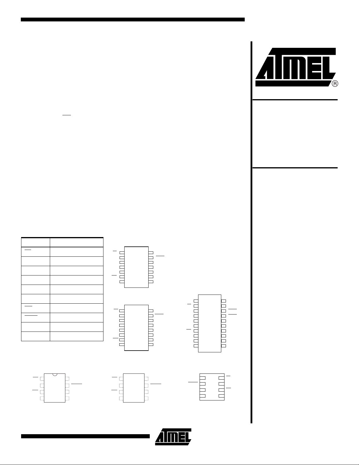
Pin Configurations
Pin Name Function
CS
SCK Serial Data Clock
SI Serial Data Input
SO Serial Data Output
GND Ground
VCC Power Supply
WP
HOLD
NC No Connect
DC Don't Connect
Chip Select
Write Protect
Suspends Serial Input
14-Lead TSSOP
1
CS
2
SO
3
NC
4
NC
5
NC
6
WP
7
GND
16-Pin SOIC
CS
1
SO
2
NC
3
NC
4
NC
5
NC
6
WP
7
GND
8
14
VCC
13
HOLD
12
NC
11
NC
10
NC
9
SCK
8
SI
20-Lead TSSOP*
NC
16
VCC
15
HOLD
14
NC
13
NC
12
NC
11
NC
10
SCK
9
SI
CS
SO
SO
NC
NC
WP
GND
DC
NC
SPI Serial
EEPROMs
128K (16,384 x 8)
256K (32,768 x 8)
AT25128
AT25256
CS
SO
WP
GND
8-Pin PDIP
8
1
7
2
3
6
4
5
VCC
HOLD
SCK
SI
CS
SO
WP
GND
8-Pin SOIC
8
1
7
2
3
6
4
5
VCC
HOLD
SCK
SI
8-Pin Leadless Array
VCC
8
HOLD
7
SCK
6
SI
5
Bottom View
*Note: Pins 3, 4 and 17, 18 are internally connected for 14-lead TSSOP socket compatibility.
CS
1
SO
2
WP
3
GND
4
Rev. 0872E–08/98
1
Page 2
space saving 8-pin PDIP (AT25128/256), 8-pin EIAJ SOIC
(AT25128/256), 8-pin and 1 6- pi n JE DEC S OI C ( A T2512 8) ,
14-pin TSSOP (AT25128), 20-pin TSSOP (AT25128/256),
and 8-pin Leadless Array (AT25128/256) packages. In
addition, the entire family is available in 5.0V (4.5V to
5.5V), 2.7V (2.7V to 5.5V) and 1.8V (1.8V to 3.6V) versions.
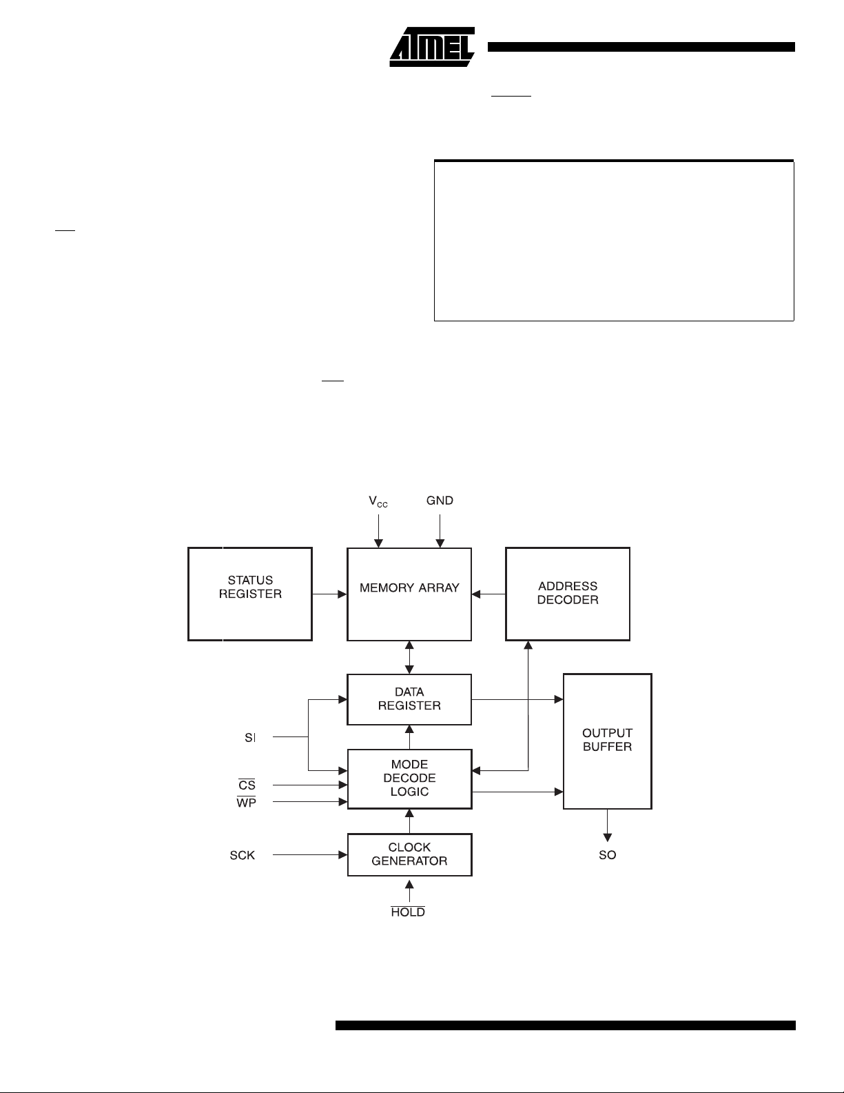
The AT25128/256 is enabled thr ough the Chip Sel ect pin
) and accessed via a 3-wire interface consisting of
(CS
Serial Data Input (SI), Serial Data Output (SO), and Serial
Clock (SCK). All progr amming cycle s are co mpletely s elftimed, and no separate ERASE cycle is required before
WRITE.
BLOCK WRITE protection is enabled by programming the
status register with top ¼, top ½ or entire array of write protection. Separate program enable and program disable
instructions are provided for additional data protection.
Hardware d ata protection is pr ovided via the WP
tect against inadvertent write attempts to the status regis-
pin to pro-
Block Diagram
ter. The HOLD
communication without resetting the serial sequence.
pin may be used to suspend any serial
Absolute Maximum Ratings*
Operating Temperature..................................-55°C to +125°C
Storage Temperature.....................................-65°C to +150°C
Voltage on Any Pin
with Respect to Ground.................................... -1.0V to +7.0V
Maximum Operating Voltage...........................................6.25V
DC Output Current........................................................5.0 mA
*NOTICE: Stresses beyond those listed under “Absolute Maxi-
mum Ratings” ma y cause permanent d amage to th e
device. This is a stress rating only and functional
operation of the device at these or any other conditions beyond those indicated in the operational sections of this specif ic ati on is n ot im pl ie d. Ex pos ure to
absolute maximum rating conditions for extended
periods may affect device reliability.
16384/32768 x 8
2
AT25128/256
Page 3
AT25128/256
Pin Capacitance
Applicable over recommended operating range from TA = 25°C, f = 1.0 MHz, VCC = +5.0V (unless otherwise noted).
Test Conditions Max Units Conditions
C
OUT
C
IN
Note: 1. This parameter is characterized and is not 100% tested.
DC Characteristics
Applicable over recommended operating range from TAI = -40°C to +85°C, VCC = +1.8V to +5.5V,
= 0°C to +70°C, VCC = +1.8V to +5.5V(unless otherwise noted).
T
AC
Symbol Parameter Test Condition Min Typ Max Units
V
CC1
V
CC2
V
CC3
I
CC1
I
CC2
I
SB1
I
SB2
I
SB3
I
IL
I
OL
(1)
V
IL
(1)
V
IH
V
OL1
V
OH1
V
OL2
V
OH2
Note: 1. V
Output Capacitance (SO) 8 pF V
Input Capacitance (CS, SCK, SI, WP, HOLD)6pFV
OUT
IN
= 0V
= 0V
Supply Voltage 1.8 3.6 V
Supply Voltage 2.7 5.5 V
Supply Voltage 4.5 5.5 V
Supply Current VCC = 5.0V at 1 MHz, SO = Open, Read 2.0 3.0 mA
Supply Current VCC = 5.0V at 2 MHz, SO = Open, Read, Write 3.0 5.0 mA
Standby Current VCC = 1.8V, CS = V
Standby Current VCC = 2.7V, CS = V
Standby Current VCC = 5.0V, CS = V
Input Leakage VIN = 0V to V
CC
CC
CC
CC
-3.0 3.0
0.1 2.0
0.2 2.0
2.0 5.0
Output Leakage VIN = 0V to VCC, TAC = 0°C to 70°C-3.0 3.0
Input Low Voltage -1.0 VCC x 0.3 V
Input High Voltage VCC x 0.7 VCC + 0.5 V
Output Low Voltage
Output High Voltage IOH = -1.6 mA vCC - 0.8 V
4.5 ≤ V
≤ 5.5V
CC
Output Low Voltage
Output High Voltage IOH = -100µAV
1.8V≤ V
and VIH max are reference only and are not tested.
IL
CC
≤3.6V
= 3.0 mA 0.4 V
I
OL
I
= 0.15mA 0.2 V
OL
- 0.2 V
CC
µ
A
µ
A
µ
A
µ
A
µ
A
3
Page 4

AC Characteristics
Applicable over recommended operating range from TA = -40°C to + 85°C, VCC = As Specified,
CL = 1 TTL Gate and 100 pF (unless otherwise noted).
Symbol Parameter Voltage Min Max Units
f
SCK
SCK Clock Frequency
4.5 - 5.5
2.7 - 5.5
1.8 - 3.6
0
0
0
3.0
2.1
0.5
MHz
t
t
t
t
t
t
t
t
RI
FI
WH
WL
CS
CSS
CSH
SU
Input Rise Time
Input Fall Time
SCK High Time
SCK Low Time
CS High Time
CS Setup Time
CS Hold Time
Data In Setup Time
4.5 - 5.5
2.7 - 5.5
1.8 - 3.6
4.5 - 5.5
2.7 - 5.5
1.8 - 3.6
4.5 - 5.5
2.7 - 5.5
1.8 - 3.6
4.5 - 5.5
2.7 - 5.5
1.8 - 3.6
4.5 - 5.5
2.7 - 5.5
1.8 - 3.6
4.5 - 5.5
2.7 - 5.5
1.8 - 3.6
4.5 - 5.5
2.7 - 5.5
1.8 - 3.6
4.5 - 5.5
2.7 - 5.5
1.8 - 3.6
150
200
800
150
200
800
250
250
1000
100
250
1000
150
250
1000
30
50
100
2
2
s
µ
2
2
2
s
µ
2
ns
ns
ns
ns
ns
ns
4.5 - 5.5
t
H
Data In Hold Time
2.7 - 5.5
1.8 - 3.6
4.5 - 5.5
t
HD
Hold Setup Time
2.7 - 5.5
1.8 - 3.6
4.5 - 5.5
t
CD
Hold Hold Time
2.7 - 5.5
1.8 - 3.6
4.5 - 5.5
t
V
Output Valid
2.7 - 5.5
1.8 - 3.6
4.5 - 5.5
t
HO
Output Hold Time
2.7 - 5.5
1.8 - 3.6
4
AT25128/256
50
50
100
100
100
400
200
300
400
0
0
0
0
0
0
150
200
800
ns
ns
ns
ns
ns
Page 5
AT25128/256
AC Characteristics (Continued)
Applicable over recommended operating range from TA = -40°C to + 85°C, VCC = As Specified,
CL = 1 TTL Gate and 100 pF (unless otherwise noted).
Symbol Parameter Voltage Min Max Units
4.5 - 5.5
t
LZ
t
HZ
t
DIS
t
WC
Endurance
Note: 1. This parameter is characterized and is not 100% tested. Contact Atmel for further information.
Hold to Output Low Z
Hold to Output High Z
Output Disable Time
Write Cycle Time
(1)
5.0V, 25°C, Page Mode 100K
2.7 - 5.5
1.8 - 3.6
4.5 - 5.5
2.7 - 5.5
1.8 - 3.6
4.5 - 5.5
2.7 - 5.5
1.8 - 3.6
4.5 - 5.5
2.7 - 5.5
1.8 - 3.6
0
0
0
100
200
300
100
200
300
200
250
1000
5
10
10
Write
Cycles
ns
ns
ns
ms
5
Page 6
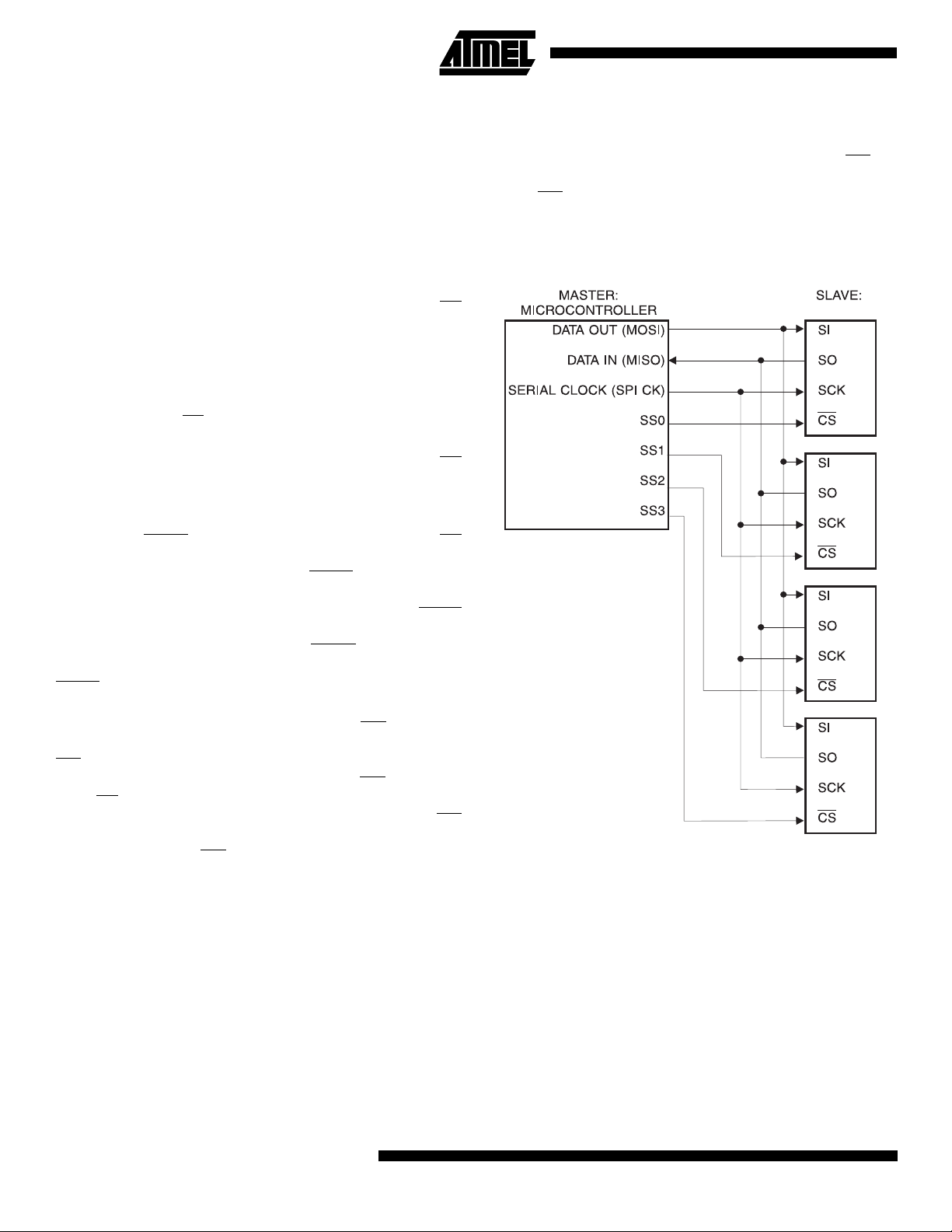
Serial Interface Description
MASTER:
SLAVE:
input, the AT25128/256 always operates as a slave.
TRANSMITTER/RECEIVER:
separate pins designated for data transmission (SO) and
reception (SI).
MSB:
transmitted and received.
SERIAL OP-CODE:
going low, the first byte will be receiv ed. This byte co ntains
the op-code that defines the operations to be performed.
INVALID OP-CODE:
data will be shifted into the AT25128/256, and the ser ial
output pin (SO) will remain in a high impedance state until
the falling edge of CS
the serial communication.
CHIP SELECT:
pin is low. When the devi ce is not s ele ct ed, d ata wi ll not b e
accepted via the SI pin, and the serial output pin (SO) will
remain in a high impedance state.
HOLD:
pin to select the AT25128/256. When the device is selected
and a serial sequence is underway, HOLD
pause the serial communication with the master device
without resetting the ser ial sequ ence. To pa use, the HOLD
pin must be brought lo w while the SCK pin is low. To
resume serial communication, the HOLD
high while the SCK pin is low (SCK may still toggle during
HOLD
is in the high impedance state.
WRITE PROTECT:
normal read/ write opera tions when he ld high. Wh en the
pin is brought low an d WPEN bit is “ 1”, all wr ite oper a-
WP
tions to the status registe r are inhibited. WP
while CS
ter. If the internal write cycle has already been initiated, WP
going low will have no effect on any write operation to the
status register. The WP
The device that generates the serial clock.
Because t he Serial Clock pin (SCK) is always an
The AT25128/256 has
The Most Significant Bit (MSB) is the first bit
After the device is selected with CS
If an invalid op-c ode i s recei ved, n o
is detected again. This will reinitialize
The AT25128/256 is selected when the CS
The HOLD
). Inputs to the SI pin will be ignored while the SO pin
is still low will interrupt a write to the status regis-
pin is us ed in conju nctio n wit h the CS
can be used to
pin is brought
The write protect pin (WP
pin function is blocked when the
) will allow
going low
WPEN bit in the statu s register is “0”. This wil l allow the
user to install the AT25128/256 in a system with the WP
tied to ground and still be able to write to the status register. All WP
set to “1”.
pin functions are enabled when the WPEN bit is
pin
SPI Serial Interface
AT25128/256
6
AT25128/256
Page 7

Functional Description
The AT25128/256 is designed to interface directly with the
synchronous serial peripheral interface (SPI) of the 6800
type series of microcontrollers.
The AT25128/256 utilizes an 8-bit instruction register. The
list of instructions and their operation codes are contained
in Table 1. All instructions, addresses, and data are transferred with the MSB first and star t with a high-to-low CS
transition..
Table 1.
Instruction
Name
WREN 0000 X110 Set Write Enable Latch
WRDI 0000 X100 Reset Write Enable Latch
RDSR 0000 X101 Read Status Regi ste r
WRSR 0000 X001 Write Status Register
READ 0000 X011 Read Data from Memory Array
WRITE 0000 X010 Write Data to Memory Array
WRITE ENABLE (WREN):
write disable state when V
instructions mus t t here fo re be p reced ed b y a Wr ite Enab le
instruction.
WRITE DISABLE (WRDI):
inadvertent writes, the Wr it e Dis able i nst ru cti on disabl es all
programming modes. The WRDI ins tructio n is ind ependen t
of the status of the WP
READ STATUS REGISTER (RDSR):
Register instruction provides access to the status register.
The READY/BUSY an d Write Enable sta tus of th e devic e
can be determined by the RDSR instruction. Similarly, the
Block Write Pr otec tion bits i ndic ate th e exten t o f prote ctio n
employed. These bits are set by using the WRSR instru ction.
Table 2.
WPEN X X X BP1 BP0 WEN RDY
Instruction Set for the AT25128/256
Instruction
Format Operation
The device will power u p in th e
is applied. All programming
CC
To protect the device against
pin.
The Read Status
Status Register Format
Bit 7 Bit 6 Bit 5 Bit 4 Bit 3 Bit 2 Bit 1 Bit 0
AT25128/256
Table 3.
Bit Definition
Bit 0 (RDY
Bit 1 (WEN) Bit 1= 0 indicates the device
Bit 2 (BP0) See Table 4.
Bit 3 (BP1) See Table 4.
Bits 4-6 are 0s when device is not in an internal write cycle.
Bit 7
(WPEN)
Bits 0-7 are 1s during an internal write cycle.
WRITE STATUS REGISTER (WRSR):
tion allows the user to select one of four levels of protection. The AT25128/256 is div ided in to four array segme nts.
Top quarter (1/4), top half (1/2), or all of the memory segments can be protected. Any of the data within any
selected segment wil l therefore be READ only. The block
write protection levels and corre sponding status register
control bits are shown in Table 4.
The three bits, BP0, BP1, and WPEN are nonvolatile cells
that have the same pro perties and functi ons as the regul ar
memory cells (e.g. WREN, t
Table 4.
Level
0 0 0 None None
1(1/4) 0 1 3000 - 3FFF 6000 - 7FFF
2(1/2) 1 0 2000 - 3FFF 4000 - 7FFF
3(All) 1 1 0000 - 3FFF 0000 - 7FFF
The WRSR instruction also allows the user to enable or
disable the write protect (WP
Write Protect Enable (WPEN) bit. Hardware write protection is ena bl e d wh en t h e W P
“1”. Hardware write protection is disabled when
WP
hardware write protected, writes to the Status Register,
including the Bloc k Protec t bits and the WPEN bi t, and the
block-protected sec tions in the memor y arra y are disab led.
Read Status Register Bit Definition
) Bit 0 = 0 (RDY) indicates the device is READY.
Bit 0 = 1 indicates the write cycle is in progress.
is not
WRITE
ENABLED. Bit 1 = 1 indicates the device is
WRITE ENABLED.
See Table 5.
The WRSR instruc-
, RDSR).
WC
Block Write Protect Bits
Array Addresses
Status Register Bits
BP1 BP0 AT25128 AT25256
Protected
) pin through the use of the
pin is low and the WPEN bit is
either
the
pin is high or the WPEN bit is “0.” When the device is
7
Page 8

Writes are only allowed to sections of the memory which
are not block-protected.
Note: When the WPEN bit is hardware write protected, it can-
not be changed bac k to “0”, as long a s the WP
low.
Table 5.
WPEN WP WEN
READ SEQUENCE (READ):
WPEN Operation
Protected
Blocks
0 X 0 Protected Protected Protected
0 X 1 Protected Writable Writable
1 Low 0 Protected Protected Protected
1 Low 1 Protected Writable Protected
X High 0 Protected Protected Protected
X High 1 P rotected W ritable Writable
Unprotected
Blocks
Reading the AT25128/25 6
pin is held
Status
Register
via the SO (Serial Output) p in requires the following
sequence. After the CS
line is pulled low to select a device,
the READ op-code is transmitted via the SI line followed by
the byte address to be rea d (Refer to Tab le 6). Upon completion, any data on the SI line will be ignored. The data
(D7-D0) at the specified address is then shifted out onto
the SO line. If only one byte is to be read, the CS
line
should be driven hig h after the da ta come s out. The READ
sequence can be continued since the byte address is automatically incremented a nd data will continue to be shifted
out. When the highest address is reached, the address
counter will roll over to the lowest address allowing the
entire memory to be read in one continuous READ cycle.
WRITE SEQUENCE (WRITE):
In order to program the
AT25128/256, two separate i ns truct ions must be executed.
First, the device
must be write enabled
via the Write
Enable (WREN) Instruction. Then a Write (WRITE) Instruc-
tion may be executed. Also, the address of the memory
location(s) to be progra mmed must be outside th e protected address field location selected by the Block Write
Protection Level. During an internal write c ycle, all commands will be ignored except the RDSR instruction.
A Write Instruc tion r equires the foll owing s equence. After
the CS
line is pulled low to select the device, the WRITE
op-code is transmitted via the S I line follo wed by the byte
address and the data (D7- D0) to be programme d (Refer to
Table 6). Programming will s tar t aft er the CS
high. (The LOW to High transition of the CS
pin is brought
pin must occur
during the SCK low ti me immedi ately after c locking in th e
D0 (LSB) data bit.
The READY/BUSY status of the devic e can be determine d
by initiating a READ STATUS REGISTER (RDSR) Instruction. If Bit 0 = 1, the WRITE cycle is still in progress. If Bit 0
= 0, the WRITE cycle has ended. Only the READ STATUS
REGISTER instruction is enabled during the WRITE programming cycle.
The AT25128/256 is capable of a 64-byte PAGE WRITE
operation. After each byte of data is received, the five low
order address bits are internally incremented by one; the
high order bits of the address will remain constant. If more
than 64-bytes of data are transmitted, the address counter
will roll over and the previously written data will be overwritten. The AT25128/256 is automatically returned to the write
disable state at the completion of a WRITE cycle.
NOTE:
If the device is not Write enabl ed (WREN), the
device will igno re the Wr it e instruction and wil l r etu rn to th e
standby state, when CS
is brought high. A new CS falli ng
edge is required to re-initiate the serial communication.
Table 6.
Address Key
Address AT25128 AT 25256
A
N
Don’t Care Bits A
A13 - A
15 - A14
0
A14 - A
0
A
15
8
AT25128/256
Page 9

Timing Diagrams (for SPI Mode 0 (0, 0))
Synchronous Data Timing
V
IH
CS
V
IL
t
CSS
V
WREN Timing
SCK
SO
IH
V
IL
t
SU
V
IH
SI
V
IL
V
OH
HI-Z
V
OL
VALID IN
t
WH
t
H
AT25128/256
t
CS
t
CSH
t
WL
t
V
t
HO
t
DIS
HI-Z
WRDI Timing
9
Page 10

RDSR Timing
CS
01234567891011121314
SCK
WRSR Timing
SO
SI
INSTRUCTION
HIGH IMPEDANCE
DATA OUT
76543210
MSB
READ Timing
10
AT25128/256
Page 11

WRITE Timing
HOLD Timing
SCK
HOLD
CS
SO
AT25128/256
t
CD
t
HD
t
HD
t
HZ
t
CD
t
LZ
11
Page 12

AT25128 Ordering Information
tWC (max)
(ms)
5 5000 5.0 3000 AT25128-10CC
ICC (max)
(µµµµA)
ISB (max)
(µµµµA)
f
MAX
(kHz) Ordering Code Package Operation Range
5000 5.0 3000 AT25128-10CI
AT25128C1-10CC
AT25128-10PC
AT25128N-10SC
AT25128W-10SC
AT25128N1-10SC
AT25128T1-10TC
AT25128T2-10TC
AT25128C1-10CI
AT25128-10PI
AT25128N-10SI
AT25128W-10SI
AT25128N1-10SI
AT25128T1-10TI
AT25128T2-10TI
8C
8C1
8P3
8S1
8S2
16S1
14T
20T
8C
8C1
8P3
8S1
8S2
16S1
14T
20T
Commercial
(0°C to 70°C)
Industrial
(-40°C to 85°C)
8C
8C1
8P3
8S1
8S2
16S1
14T
20T
Blank
-2.7
-1.8
12
Package Type
8-Lead, 0.230" Wide, Leadless Array Package (LAP)
8-Lead, 0.300" Wide, Leadless Array Package (LAP)
8-Lead, 0.300" Wide, Plastic Dual In-line Package (PDIP)
8-Lead, 0.150" Wide, Plastic Gull Wing Small Outline Package (JEDEC SOIC)
8-Lead, 0.200" Wide, Plastic Gull Wing Small Outline Package (EIAJ SOIC)
16-Lead, 0.150" Wide, Plastic Gull Wing Small Outline Package (JEDEC SOIC)
14-Lead, 0.170" Wide, Thin Shrink Small Outline Package (TSSOP)
20-Lead, 0.170" Wide, Thin Shrink Small Outline Package (TSSOP)
Options
Standard Device (4.5V to 5.5V)
Low Voltage (2.7V to 5.5V)
Low Voltage (1.8V to 3.6V)
AT25128/256
Page 13

AT25128 Ordering Information (Continued)
tWC (max)
(ms)
10 2000 2.0 2100 AT25128-10CC-2.7
ICC (max)
(µµµµA)
ISB (max)
(µµµµA)
f
MAX
(kHz) Ordering Code Package Operation Range
AT25128C1-10CC-2.7
AT25128-10PC-2.7
AT25128N-10SC-2.7
AT25128W-10SC-2.7
AT25128N1-10SC-2.7
AT25128T1-10TC-2.7
AT25128T2-10TC-2.7
2000 2.0 2100 AT25128-10CI-2.7
AT25128C1-10CI-2.7
AT25128-10PI-2.7
AT25128N-10SI-2.7
AT25128W-10SI-2.7
AT25128N1-10SI-2.7
AT25128T1-10TI-2.7
AT25128T2-10TI-2.7
AT25128/256
8C
8C1
8P3
8S1
8S2
16S1
14T
20T
8C
8C1
8P3
8S1
8S2
16S1
14T
20T
Commercial
(0°C to 70°C)
Industrial
(-40°C to 85°C)
8C
8C1
8P3
8S1
8S2
16S1
14T
20T
Blank
-2.7
-1.8
Package Type
8-Lead, 0.230" Wide, Leadless Array Package (LAP)
8-Lead, 0.300" Wide, Leadless Array Package (LAP)
8-Lead, 0.300" Wide, Plastic Dual In-line Package (PDIP)
8-Lead, 0.150" Wide, Plastic Gull Wing Small Outline Package (JEDEC SOIC)
8-Lead, 0.200" Wide, Plastic Gull Wing Small Outline Package (EIAJ SOIC)
16-Lead, 0.150" Wide, Plastic Gull Wing Small Outline Package (JEDEC SOIC)
14-Lead, 0.170" Wide, Thin Shrink Small Outline Package (TSSOP)
20-Lead, 0.170" Wide, Thin Shrink Small Outline Package (TSSOP)
Options
Standard Device (4.5V to 5.5V)
Low Voltage (2.7V to 5.5V)
Low Voltage (1.8V to 3.6V)
13
Page 14

AT25128 Ordering Information (Continued)
tWC (max)
(ms)
10 1000 2.0 500 AT25128-10CC-1.8
ICC (max)
(µµµµA)
ISB (max)
(µµµµA)
f
MAX
(kHz) Ordering Code Package Operation Range
AT25128C1-10CC-1.8
AT25128-10PC-1.8
AT25128N-10SC-1.8
AT25128W-10SC-1.8
AT25128N1-10SC-1.8
AT25128T1-10TC-1.8
AT25128T2-10TC-1.8
1000 2.0 500 AT25128-10CI-1.8
AT25128C1-10CI-1.8
AT25128-10PI-1.8
AT25128N-10SI-1.8
AT25128W-10SI-1.8
AT25128N1-10SI-1.8
AT25128T1-10TI-1.8
AT25128T2-10TI-1.8
8C
8C1
8P3
8S1
8S2
16S1
14T
20T
8C
8C1
8P3
8S1
8S2
16S1
14T
20T
Commercial
(0°C to 70°C)
Industrial
(-40°C to 85°C)
8C
8C1
8P3
8S1
8S2
16S1
14T
20T
Blank
-2.7
-1.8
14
Package Type
8-Lead, 0.230" Wide, Leadless Array Package (LAP)
8-Lead, 0.300" Wide, Leadless Array Package (LAP)
8-Lead, 0.300" Wide, Plastic Dual In-line Package (PDIP)
8-Lead, 0.150" Wide, Plastic Gull Wing Small Outline Package (JEDEC SOIC)
8-Lead, 0.200" Wide, Plastic Gull Wing Small Outline Package (EIAJ SOIC)
16-Lead, 0.150" Wide, Plastic Gull Wing Small Outline Package (JEDEC SOIC)
14-Lead, 0.170" Wide, Thin Shrink Small Outline Package (TSSOP)
20-Lead, 0.170" Wide, Thin Shrink Small Outline Package (TSSOP)
Options
Standard Device (4.5V to 5.5V)
Low Voltage (2.7V to 5.5V)
Low Voltage (1.8V to 3.6V)
AT25128/256
Page 15

AT25256 Ordering Information
tWC (max)
(ms)
5 5000 5.0 3000 AT25256-10CC
10 2000 2.0 2100 AT25256-10CC-2.7
10 1000 2.0 500 AT25256-10CC-1.8
ICC (max)
(µA)
ISB (max)
(µA)
f
MAX
(kHz) Ordering Code Package Operation Range
AT25256C1-10CC
AT25256-10PC
AT25256W-10SC
AT25256T2-10TC
5000 5.0 3000 AT25256-10CI
AT25256C1-10CI
AT25256-10PI
AT25256W-10SI
AT25256T2-10TI
AT25256C1-10CC-2.7
AT25256-10PC-2.7
AT25256W-10SC-2.7
AT25256T2-10TC-2.7
2000 2.0 2100 AT25256-10CI-2.7
AT25256C1-10CI-2.7
AT25256-10PI-2.7
AT25256W-10SI-2.7
AT25256T2-10TI-2.7
AT25256C1-10CC-1.8
AT25256-10PC-1.8
AT25256W-10SC-1.8
AT25256T2-10TC-1.8
1000 2.0 500 AT25256-10CI-1.8
AT25256C1-10CI-1.8
AT25256-10PI-1.8
AT25256W-10SI-1.8
AT25256T2-10TI-1.8
AT25128/256
8C
8C1
8P3
8S2
20T
8C
8C1
8P3
8S2
20T
8C
8C1
8P3
8S2
20T
8C
8C1
8P3
8S2
20T
8C
8C1
8P3
8S2
20T
8C
8C1
8P3
8S2
20T
Commercial
(0°C to 70°C)
Industrial
(-40°C to 85°C)
Commercial
(0°C to 70°C)
Industrial
(-40°C to 85°C)
Commercial
(0°C to 70°C)
Industrial
(-40°C to 85°C)
8C
8C1
8P3
8S2
20T
Blank
-2.7
-1.8
Package Type
8-Lead, 0.230" Wide, Leadless Array Package (LAP)
8-Lead, 0.300" Wide, Leadless Array Package (LAP)
8-Lead, 0.300" Wide, Plastic Dual In-line Package (PDIP)
8-Lead, 0.200" Wide, Plastic Gull Wing Small Outline Package (EIAJ SOIC)
20-Lead, 0.170" Wide, Thin Shrink Small Outline Package (TSSOP)
Options
Standard Device (4.5V to 5.5V)
Low Voltage (2.7V to 5.5V)
Low Voltage (1.8V to 3.6V)
15
Page 16

Packaging Information
8C
, 8-Lead, 0.230" Wide, Leadless Array Package
(LAP)
Dimensions in Inches and (Millimeters)
SIDE
5.15 (0.203)
4.85 (0.191)
1.27 (0.050) TYP
TOP VIEW
6.15 (0.242)
5.85 (0.230)
BOTTOM VIEW
8
7
6
5
0.64 (0.025) TYP
1
2
3
4
VIEW
0.41 (0.016) TYP
1.30 (0.051)
1.00 (0.039)
0.42 (0.017)
0.34 (0.013)
8C1
, 8-Lead, 0.300" Wide, Leadless Array Package
(LAP)
Dimensions in Inches and (Millimeters)
SIDE
5.15 (0.203)
4.85 (0.191)
1.27 (0.050) TYP
TOP VIEW
8.15 (0.321)
7.85 (0.309)
BOTTOM VIEW
8
7
6
5
0.64 (0.025) TYP
1
2
3
4
VIEW
0.41 (0.016) TYP
1.30 (0.051)
1.00 (0.039)
0.42 (0.017)
0.34 (0.013)
8P3
, 8-Lead, 0.300" Wide, Plastic Dual In-line
Package (PDIP)
Dimensions in Inches and (Millimeters)
JEDEC STANDARD MS-001 BA
.400 (10.16)
.355 (9.02)
PIN
1
.280 (7.11)
.240 (6.10)
.037 (.940)
.300 (7.62) REF
.210 (5.33) MAX
SEATING
PLANE
.150 (3.81)
.115 (2.92)
.012 (.305)
.008 (.203)
.070 (1.78)
.045 (1.14)
.027 (.690)
.100 (2.54) BSC
.015 (.380) MIN
.022 (.559)
.014 (.356)
.325 (8.26)
.300 (7.62)
0
REF
15
.430 (10.9) MAX
8S1
, 8-Lead, 0.150" Wide, Plastic Gull Wing Small
Outline (JEDEC SOIC)
Dimensions in Inches and (Millimeters)
.020 (.508)
.013 (.330)
.244 (6.20)
.228 (5.79)
.068 (1.73)
.053 (1.35)
.010 (.254)
.007 (.203)
PIN 1
0
8
.157 (3.99)
.150 (3.81)
.050 (1.27) BSC
.196 (4.98)
.189 (4.80)
.010 (.254)
.004 (.102)
REF
.050 (1.27)
.016 (.406)
16
AT25128/256
Page 17

Packaging Information
AT25128/256
8S2
, 8-Lead, 0.200" Wide, Plastic Gull Wing Small
Outline (EIAJ SOIC)
Dimensions in Inches and (Millimeters)
.020 (.508)
.012 (.305)
PIN 1
0
REF
8
.213 (5.41)
.205 (5.21)
.050 (1.27) BSC
.212 (5.38)
.203 (5.16)
.013 (.330)
.004 (.102)
.035 (.889)
.020 (.508)
.330 (8.38)
.300 (7.62)
.080 (2.03)
.070 (1.78)
.010 (.254)
.007 (.178)
16S1
, 16-Lead, 0.150" Wide, Plastic Gull Wing Small
Outline (JEDEC SOIC)
Dimensions in Inches and (Millimeters)
0.020 (0.51)
0.013 (0.33)
0.069 (1.75)
0.053 (1.35)
0.244 (6.20)
0.228 (5.80)
PIN 1
0.158 (4.00)
0.150 (3.80)
.050 (1.27) BSC
0.394 (10.00)
0.386 (09.80)
0.010 (0.25)
0.004 (0.10)
0
REF
8
0.050 (1.27)
0.016 (0.40)
0.010 (0.25)
0.008 (0.19)
14T
, 14-Lead, 0.170" Wide, Thin Shrink Small
Outline Package (TSSOP)
Dimensions in Millimeters and (Inches)*
4.50 (.177)
4.30 (.169)
1.20 (.047) MAX
0.20 (.008)
0.09 (.004)
INDEX MARK
.650 (.026) BSC
0
REF
8
5.10 (.201)
4.90 (.193)
0.30 (.012)
0.19 (.007)
0.75 (.030)
0.45 (.018)
PIN
1
0.15 (.006)
0.05 (.002)
*Controlling dimension: millimeters
6.50 (.256)
6.25 (.246)
SEATING
PLANE
20T
, 20-Lead, 0.170" Wide, Thin Shrink Small
Outline Package (TSSOP)
Dimensions in Millimeters and (Inches)*
4.50 (.177)
4.30 (.169)
1.20 (.047) MAX
0.20 (.008)
0.09 (.004)
INDEX MARK
.650 (.026) BSC
0
REF
8
6.60 (.260)
6.40 (.252)
0.30 (.012)
0.19 (.007)
0.75 (.030)
0.45 (.018)
PIN
1
0.15 (.006)
0.05 (.002)
*Controlling dimension: millimeters
6.50 (.256)
6.25 (.246)
SEATING
PLANE
17
 Loading...