

Datasheet AT25128N1-10SI-2.7, AT25128N1-10SI-1.8, AT25128N1-10SI, AT25128N1-10SC-2.7, AT25128N1-10SC-1.8 Datasheet (ATMEL)
...Page 1
SPI Serial
E2PROMs
128K (16384 x 8)
AT25128
Preliminary
Features
Serial Peripheral Inte rfac e (SPI) Compatible
•
Supports SPI Modes 0 (0, 0) an d 3 (1, 1)
•
Low Voltage and Standard Voltage Operation
•
5.0 (VCC = 4.5V to 5.5V)
2.7 (VCC = 2.7V to 5.5V)
1.8 (VCC = 1.8V to 3.6V)
2.1 MHz Clock Rate
•
32-Byte Page Mode
•
Block Write Protection
•
Protect 1/4, 1/2, or Entire Array
Write Protect (WP) Pin and Write Disa bl e Instructions for
•
Both Hardware and Software Data Protection
Self-Timed Write Cycle (5 ms Typical)
•
High Reliabili ty
•
Endurance: 100, 000 Cycles
Data Retention: 100 Years
Automotive Grade and Extended Temperature Dev ic es Available
•
8-Pin PDIP, 14-pin, 16-pi n JEDEC SOIC, and 20-Pi n TSSOP Pac ka ge s
•
Description
The AT25128 provides 131,072 bits of serial electrically erasable programmable read
only memory (EEPROM) organized as 16,384 words of 8 bits each. The device is
optimized for use in many industrial and commercial applications where low power
and low voltage operation are essential. The AT25128 is available in space saving
8-pin PDIP, JEDEC SOIC, and 14-pin and 20-pin TSSOP packages.
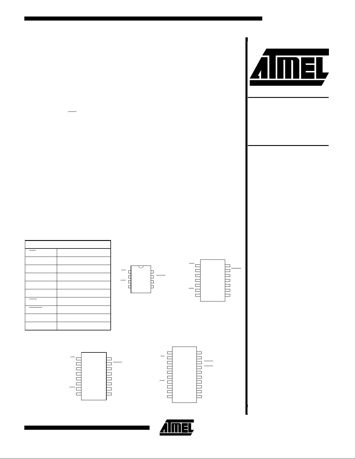
Pin Configurations
Pin Name Function
CS Chip Select
SCK Serial Data Clock
SI Serial Data Input
SO S eri al Data Out put
GND Ground
V
CC
WP Write Protect
Power Supply
HOLD Suspends Serial Input
NC No Connec t
DC Don’ t Connect
CS
SO
NC
NC
NC
NC
WP
GND
16-Lead SOIC
1
2
3
4
5
6
7
8
16
15
14
13
12
11
10
9
CS
SO
WP
GND
VCC
HOLD
NC
NC
NC
NC
SCK
SI
8-Pin PDIP
1
8
2
7
3
6
4
5
VCC
HOLD
SCK
SI
20-Lead TSSOP*
1
NC
2
CS
3
SO
4
SO
5
NC
6
NC
7
WP
8
GND
9
DC
10
NC
14-Pin SOIC
CS
1
SO
2
NC
3
NC
4
NC
5
WP
6
GND
7
20
NC
19
VCC
18
HOLD
17
HOLD
16
NC
15
NC
14
SCK
13
SI
12
DC
11
NC
(continued)
14
VCC
13
HOLD
12
NC
11
NC
10
NC
9
SCK
8
SI
* Note: Pins 3, 4 and 17, 18 are internally connected for 14-lead TSSO P sock et com pati bil it y.
Page 2
Description (Continued)
The AT25128 is enabled through the Chip Select pin ( CS)
and accessed via a 3-wire interface consisting of Serial
Data Input (SI), Serial Data Output (SO), and Serial Clock
(SCK). All programming cycles are completely self-timed,
and no separate ERASE cycle is required before WRITE.
BLOCK WRITE protection is enabled by programming the
status register with one of four blocks of write protection.
Separate prog ram enable and program disab le instruc-
Absolute Maximum Rat ings*
Operating Temperature...................-55°C to +125°C
Storage Temperature...................... -65°C to +150°C
Voltage on Any Pin
with Respect to Ground ..................... -1.0V to +7.0V
Maximum Operating Voltage ........................... 6.25V
DC Output Current.........................................5.0 mA
tions are provided for additional data protection. Hardware
data protection is provided via the
against inadvertent write attempts to the status register.
HOLD pin may be used to suspend any serial commu-
The
nication without resetting the serial sequence.
*NOTICE: Stresses beyond those listed unde r “Absolu te Maxi-
mum Ratings” may cause permanent da ma ge to th e de vice .
This is a stress rating only and functional operation of the
device at these or any other conditions beyond those indicated in the operational sections of this specification is not
implied. Exposure to absolute maximu m rat ing conditions
for extended periods may affect device reliability.
WP pin to protect
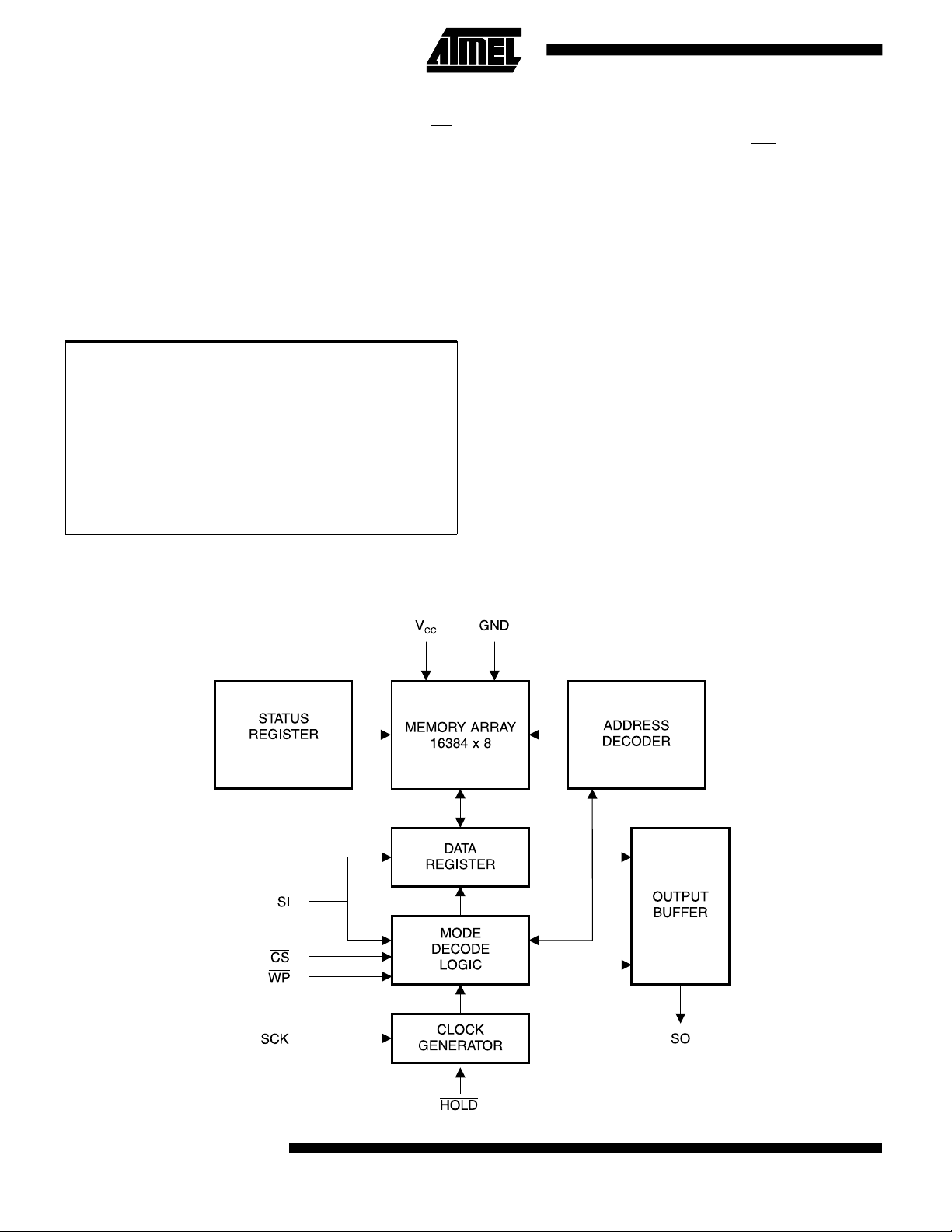
Block Diagram
2 AT25128
Page 3

AT25128
Pin Capacitance
(1)
Applicable over recommended operating range from TA = 25°C, f = 1.0 MHz, VCC = +5.0V (unless otherwise noted).
Test Conditions Max Units Conditions
C
OUT
C
IN
Note: 1. This parameter is characte riz ed and is no t 10 0% tes te d.
Output Capacitance (SO) 8 pF V
Input Capacitance (CS, SCK, SI, WP, HOLD) 6 pF VIN = 0V
OUT
= 0V
DC Characteristics
Applicable over recommended operating range from: TAI = -40°C to +85°C, VCC = +1.8V to +5.5V,
= 0°C to +70°C, VCC = +1.8V to +5.5V (unless otherwise noted).
T
AC
Symbol Parameter Test Condition Min Typ Max Units
V
Supply Voltage 1.8 3.6 V
CC1
V
CC2
V
CC3
I
CC1
I
CC2
Standby Current VCC = 1.8V CS = V
I
SB1
I
SB2
I
SB3
I
IL
I
OL
(1)
V
IL
(1)
V
IH
V
OL1
V
OH1
V
OL2
V
OH2
Note: 1. VIL min and VIH max are reference only and are not tested.
Supply Voltage 2.7 5.5 V
Supply Voltage 4.5 5.5 V
= 5.0V at 1 MHz,
V
Supply Current
Supply Current
CC
SO = Open
= 5.0V at 2 MHz,
V
CC
SO = Open
Standby Current VCC = 2.7V CS = V
Standby Current VCC = 5.0V CS = V
CC
CC
CC
0.2 0.5 µA
0.5 2.0 µA
3.0 mA
5.0 mA
0.1 µA
Input Leakage VIN = 0V to VCC -3.0 3.0 µA
= 0V to VCC,
V
Output Leakage
Input Low Voltage -1.0 V
IN
T
= 0°C to 70°C
AC
-3.0 3.0 µA
x 0.3 V
CC
Input High Voltage VCC x 0.7 VCC + 0.5 V
Output Low Voltage
4.5V ≤ V
Output High Voltage IOH = -1.6 mA VCC - 0.8 V
Output Low Voltage
1.8V ≤ V
Output High Voltage IOH = -100 µAVCC - 0.2 V
≤ 5.5V
CC
≤ 3.6V
CC
I
= 3.0 mA 0.4 V
OL
I
= 0.15 mA 0.2 V
OL
3
Page 4

AC Characteristics
Applicable over recommended operating range from TA = -40°C to +85°C, VCC = As Specified,
CL = 1 TTL Gate and 100 pF (unless otherwise noted).
Symbol Parameter Voltage Min Max Units
2.1
2.1
0.5
2
2
2
2
2
2
200
200
800
100
100
100
MHz
f
SCK
t
RI
t
FI
t
WH
t
WL
t
CS
t
CSS
t
CSH
t
SU
t
H
t
HD
t
CD
t
V
t
HO
t
LZ
SCK Clock Frequency
Input Rise Time
Input Fall Time
SCK High Time
SCK Low Time
CS High Time
CS Setup Time
CS Hold Time
Data In Setup Time
Data In Hold Time
Hold Setup Time
Hold Hold Time
Output Valid
Output Hold Time
Hold to Output Low Z
4.5 - 5.5
2.7 - 5.5
1.8 - 3.6
4.5 - 5.5
2.7 - 5.5
1.8 - 3.6
4.5 - 5.5
2.7 - 5.5
1.8 - 3.6
4.5 - 5.5
2.7 - 5.5
1.8 - 3.6
4.5 - 5.5
2.7 - 5.5
1.8 - 3.6
4.5 - 5.5
2.7 - 5.5
1.8 - 3.6
4.5 - 5.5
2.7 - 5.5
1.8 - 3.6
4.5 - 5.5
2.7 - 5.5
1.8 - 3.6
4.5 - 5.5
2.7 - 5.5
1.8 - 3.6
4.5 - 5.5
2.7 - 5.5
1.8 - 3.6
4.5 - 5.5
2.7 - 5.5
1.8 - 3.6
4.5 - 5.5
2.7 - 5.5
1.8 - 3.6
4.5 - 5.5
2.7 - 5.5
1.8 - 3.6
4.5 - 5.5
2.7 - 5.5
1.8 - 3.6
4.5 - 5.5
2.7 - 5.5
1.8 - 3.6
0
0
0
200
300
800
200
200
800
250
250
1000
250
250
1000
250
250
1000
50
50
100
50
50
100
100
100
400
100
100
400
0
0
0
0
0
0
0
0
0
µs
µs
ns
ns
ns
ns
ns
ns
ns
ns
ns
ns
ns
ns
4 AT25128
(continued)
Page 5

AT25128
AC Characteristics (Continued)
Symbol Parameter Voltage Min Max Units
100
100
100
250
250
1000
5
10
20
t
HZ
t
DIS
t
WC
Hold to Output High Z
Output Disable Time
Write Cycle Time
4.5 - 5.5
2.7 - 5.5
1.8 - 3.6
4.5 - 5.5
2.7 - 5.5
1.8 - 3.6
4.5 - 5.5
2.7 - 5.5
1.8 - 3.6
ns
ns
ms
5
Page 6

Serial Interface Description
MASTER: The device that generates the serial clock.
SLAVE: Because the Serial Clock pin (SCK) is always
an input, the AT25128 always operates as a slave.
TRANSMITTER/RECEIVER: The AT25128 has
separate pins designated for data transmission (SO) and
reception (SI).
MSB: The Most Significant Bit (MSB) is the first bit
transmitted and received.
SERIAL OP-CODE: After the device is selected with CS
going low, the first byte will be received. This byte contains
the op-code that defines the operations to be performed.
INVALID OP-CODE: If an invalid op-code is received,
no data will be shifted into the AT25128, and the serial
output pin (SO) will remain in a high impedance state until
the falling edge of
ize the serial communication.
CHIP SELECT: The AT25128 is selected when the
pin is low. When the device is not selected, data will not be
accepted via the SI pin, and the serial output pin (SO) will
remain in a high impedance state.
HOLD: The
pin to select the AT25128. When the device is selected
and a serial sequence is underway,
pause the serial communication with the master device
without resetting the serial sequence. To pause, the
HOLD pin must be brought low while the SCK pin is low.
To resume serial communication, the
high while the SCK pin is low (SCK may still toggle during
HOLD). Inputs to the SI pin will be ignored while the SO
pin is in the high impedance state.
WRITE PROTECT: The write protect pin (
normal read/write operations when held high. When the
WP pin is brought low and WPEN bit is “1", all write operations to the status register are inhibited.
CS is still low will interrupt a write to the status reg-
while
ister. If the internal write cycle has already been initiated,
WP going low will have no effect on any write operation to
the status register. The
the WPEN bit in the status register is ”0". This will allow the
user to install the AT25128 in a system with the
tied to ground and still be able to write to the status register. All
is set to “1".
WP pin functions are enabled when the WPEN bit
CS is detected again. This will reinitial-
CS
HOLD pin is used in conjunction with the CS
HOLD can be used to
HOLD pin is brought
WP) will allow
WP going low
WP pin function is blocked when
WP pin
SPI Serial Interface
6 AT25128
Page 7

AT25128
Functional Description
The AT25128 is designed to interface directly with the synchronous serial peripheral interface (SPI) of the 6805 and
68HC11 series of microcontrollers.
The AT25128 utilizes an 8 bit instruction register. The list
of instructions and their operation codes are contained in
Table 1. All instructions, addresses, and data are transferred with the MSB first.
Table 1. Instruction Set for the AT25128
Instruction
Name
WREN 0000 X110 Set Write Enable Latch
WRDI 0000 X100 Reset Write Enable Latch
RDSR 0000 X101 Read Status Register
WRSR 0000 X001 Write Status Register
READ 0000 X011 Rea d Dat a from Memory Array
WRITE 0000 X010 Write Data to Me mo ry Array
WRITE ENABLE (WREN): The device will power up in
the write disable state when V
ming instructions must therefore be preceded by a Write
Enable instruction.
WRITE DISABLE (WRDI): To protect the device
against inadvertent writes, the Write Disable instruction
disables all programming modes. The WRDI instruction is
independent of the status of the
READ STATUS REGISTER (RDSR): The Read Status
Register instruction provides access to the status r egister.
The READY/BUSY and Write Enable status of the device
can be determined by the RDSR instruction. Similarly, the
Block Write Protection bits indicate the extent of protection
employed. These bits are set by using the WRSR instruction.
Table 2a. Status Register Format
Bit 7 Bit 6 Bit 5 Bit 4 Bit 3 Bit 2 Bit 1 Bit 0
WPEN X X X BP1 BP0 WEN RDY
Instruction
Format Operation
is applied. All program-
CC
WP pin.
Table 2b. Read Status Register Bit Definition
Bit Definition
Bit 0 (RDY)
Bit 1 (WEN)
Bit 2 (BP0) See Table 3.
Bit 3 (BP1) See Table 3.
Bits 4-6 are 0s when device is not in an internal write cycle.
Bit 7 (WPEN) See Table 4.
Bits 0-7 are 1s during an internal write cycle.
Bit 0 = 0 (RDY) indicates the device is
READY. Bit 0 = 1 indicates the write cycle is
in progress.
Bit 1= 0 indicates the device
ENABLED. Bit 1 = 1 indicates the device is
WRITE ENABLED.
is not
WRITE
WRITE STATUS REGISTER (WRSR): The WRSR instruction allows the user to select one of four levels of protection. The AT25128 is divided into four array segments.
One quarter (1/4), one half (1/2), or all of the memory segments can be protected. Any of the data within any selected segmen t will therefore be READ only. The block
write protection levels and corresponding status register
control bits are shown in Table 3.
The three bits, BP0, BP1, and WPEN are nonvolatile cells
that have the same properties and functions as the regular
memory cells (e.g. WREN, t
, RDSR).
WC
Table 3. Block Write Protect Bits
Status
Level
0 0 0 None
1(1/4) 0 1 3000 - 3FFF
2(1/2) 1 0 2000 - 3FFF
3(All) 1 1 0000 - 3FFF
Register
Bits
BP1 BP0 AT25128
Array Addresses Protected
The WRSR instruction also allows the user to enable or
disable the write protect (
WP) pin through the use of the
Write Protect Enable (WPEN) bit. Hardware write protection is enabled when the
is “1.” Hardware write protection is disabled when
WP pin is low and the WPEN bit
either
the W P pin is high or the WPEN bit is “0.” When the device
is hardware write protected, writes to the Status Register,
including the Block Protect bits and the WPEN bit, and the
block-protected sections in the memory array are disabled. Writes are only allowed to sections of the memory
which are not block-protected.
NOTE: When the WPEN bit is hardware write pr otected, it
cannot be changed back to “0,” as long as the
WP pin is
held low.
(continued)
7
Page 8

Functional Description (Continued)
Table 4. WPEN Operation
Protected
WPEN WP WEN
0 X 0 Protected Protected Protected
0 X 1 Protected Writable Writable
1 Low 0 Protected Protected Protected
1 Low 1 Protected Writable Protected
X High 0 Protected Protected Protected
X High 1 Protected Writable Writable
Blocks
READ SEQUENCE (READ): Reading the AT25128 via
the SO (Serial Output) pin requires the following sequence. After the
CS line is pulled low to select a device,
the READ op-code is transmitted via the SI line followed
by the byte address to be read (A15-A0, Refer to Table 5).
Upon completion, any data on the SI line will be ignored.
The data (D7-D0) at the specified address is then shifted
out onto the SO line. If only one byte is to be read, the
line should be driven high after the data comes out. The
READ sequence can be continued since the byte address
is automatically incremented and data will continue to be
shifted out. When the highest address is reached, the address counter will roll over to the lowest address allowing
the entire memory to be read in one continuous READ cycle.
WRITE SEQUENCE (WRITE): In order to program the
AT25128, two separate instructions must be executed.
First, the device must be write enabled via the Write En-
able (WREN) Instruction. Then a Write (WRITE) Instruction may be executed. Also, the address of the memory
location(s) to be programmed must be outside the protected address field location selected by the Block Write
Protection Level. During an internal write cycle, all commands will be ignored except the RDSR instruction.
A Write Instruction requires the following sequence. After
CS line is pulled low to select the device, the WRITE
the
op-code is transmitted via the SI line followed by the byte
address (A15-A0) and the data (D7-D0) to be programmed (Refer to Table 5). Programming will start after
CS pin is brought high. (The LOW to High transition of
the
CS pin must occur during the SCK low time immedi-
the
ately after clocking in the D0 (LSB) data bit.
Unprotected
Blocks
Status
Register
CS
The READY/BUSY status of the device can be determined by initiating a READ STATUS REGISTER (RDSR)
Instruction. If Bit 0 = 1, the WRITE cycle is still in progress.
If Bit 0 = 0, the WRITE cycle has ended. Only the READ
STATUS REGISTER instruction is enabled during the
WRITE programming cycle.
The AT25128 is capable of a 32-byte PAGE WRITE operation. After each byte of data is received, the five low
order address bits are internally incremented by one; the
high order bits of the address will remain constant. If mor e
than 32-bytes of data are transmitted, the address counter
will roll over and the previously written data will be overwritten. The AT25128 is automatically returned to the write
disable state at the completion of a WRITE cycle.
NOTE: If the device is not Write enabled (WREN), the device will ignore the Write instruction and will return to the
standby state, when
CS is brought high. A new CS falling
edge is required to re-initiate the serial communication.
Table 5. Address Key
Address AT25128
A
N
Don’t Care Bits A15 - A
A13 - A
0
14
8 AT25128
Page 9

Timing Diagrams (for SPI Mode 0 (0,0))
Synchronous Data Tim in g
V
IH
CS
V
IL
t
CSS
V
SCK
SO
IH
V
IL
t
SU
V
IH
SI
V
IL
V
OH
HI-Z
V
OL
VALID IN
t
WH
t
H
AT25128
t
CS
t
CSH
t
WL
t
V
t
HO
t
DIS
HI-Z
WREN Timing
WRDI Timing
9
Page 10

RDSR Timing
CS
01234567891011121314
SCK
INSTRUCTION
SI
WRSR Timing
READ Timing
SO
HIGH IMPEDANCE
DATA OUT
76543210
MSB
10 AT25128
Page 11

WRITE Timing
HOLD Timing
AT25128
CS
SCK
HOLD
SO
t
CD
t
HD
t
HD
t
HZ
t
CD
t
LZ
11
Page 12

Ordering Information
tWC (max)
(ms)
ICC (max)
(µA)
ISB (max)
(µA)
f
MAX
(kHz)
Ordering Code Package Operation Range
5 5000 2.0 2100 AT25128-10PC 8P3 Commercial
AT25128-10SC 14S (0°C to 70°C)
AT25128N1-10SC 16S1
AT25640T2-10TC 20T
10 3000 0.5 2100 AT25128-10PC-2.7 8P3 Commercial
AT25128-10SC-2.7 14S (0°C to 70°C)
AT25128N1-10SC-2.7 16S1
AT25128T2-10TC-2.7 20T
20 3000 0.2 500 AT25128-10PC-1.8 8P3 Commercial
AT25128-10SC-1.8 14S (0°C to 70°C)
AT25128N1-10SC-1.8 16S1
AT25128T2-10TC-1.8 20T
5 5000 2.0 2100 AT25128-10PI 8P3 Industrial
AT25128-10SI 14S (-40°C to 85°C)
AT25128N1-10SI 16S1
AT25128T2-10TI 20T
10 3000 0.5 2100 AT25128-10PI-2.7 8P3 Industrial
AT25128-10SI-2.7 14S (-40°C to 85°C)
AT25128N1-10SI-2.7 16S1
AT25128T2-10TI-2.7 20T
20 3000 0.2 500 AT25128-10PI-1.8 8P3 Industrial
AT25128-10SI-1.8 14S (-40°C to 85°C)
AT25128N1-10SI-1.8 16S1
AT25128T2-10TI-1.8 20T
Package Type
8P3 8-Lead, 0.300" Wide, Plastic Dual Inli ne Pack age (PDIP)
14S 14-Lead, 0.150" Wide, Plastic Gull Win g Small Outl ine Pac ka ge (JEDEC SOIC)
16S1 16-Lead, 0.150" Wide, Pla st ic Gu ll Win g Small Outl ine Pac ka ge (JEDEC SOIC)
20T 20-Lead, 0.170" Wide, Thin Supe r Small Out li ne Pack age (TSSOP)
Options
Blank Standard Device (4.5V to 5.5 V )
-2.7 Low Voltage (2.7V to 5.5V)
-1.8 Low Voltage (1.8V to 3.6V)
12 AT25128
 Loading...