

Page 1
AT2101
12-Bit 6MSPS A/D CONVERTER
Features
˙Resolution: 12-Bit ± 0.5 LSB(DNL)
˙Maximum Conversion Rate: 6 MSPS
˙Built-in Sample and Hold Function
˙Built-in Reference Voltage
˙Single +5.0 V Power Supply
˙Three-State TTL Compatible Output
˙No Missing Code
Applications
˙Video Digitizing
˙Personal Computer Video
˙Multimedia
˙Digital Television
General Description
The AT2101 is a pipeline CMOS analog-todigital converter with modified coding algorithm
and capable of digitizing full-scale analog input
signals into 12-bit digital words at sample rate of
6 MSPS.
This high performance converter includes a 12bit quantizer, high bandwidth sample/hold, and
an internal reference, which eliminates the need
for external reference circuitry. The AT2101
employs digital error correction techniques to
provide excellent differential linearity for
imaging applications.
The AT2101 operates from a single +5.0V power
supply. All digital inputs are CMOS compatible
and the tri-state outputs are TTL-compatible. The
AT2101 is ideal for most video and image
processing applications that require low power
dissipation and low cost.
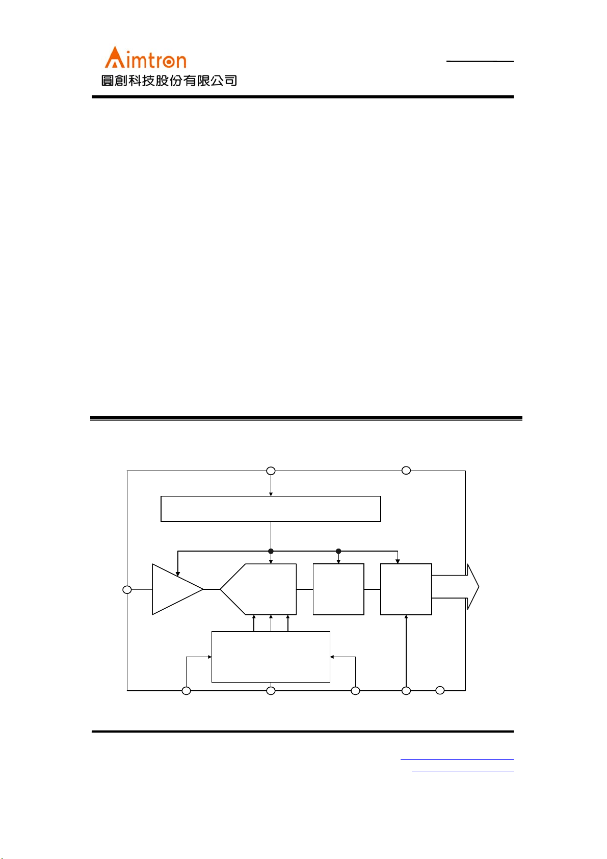
Block Diagram
VIN
S/H
AVDD
CLK
Timing Circuitry
12-Bit
Pipelined
A/D Core
VRT
3.5V
Internal Reference Generator
VCM
VRB
1.5V
Modified
Coding
algorithm
AGND
DVDD
3-State
Output
/OE
D0
.
.
D11
DGND
2F, No.10, Prosperity RD. II, Science-Based Industrial Park, Hsinchu 300,Taiwan, R.O.C.
Tel: 886-3-563-0878 WWW: http://www.aimtron.com.tw
Fax: 886-3-563-0879 Email: service@aimtron.com.tw
1
Page 2
AT2101
12-Bit 6MSPS A/D CONVERTER
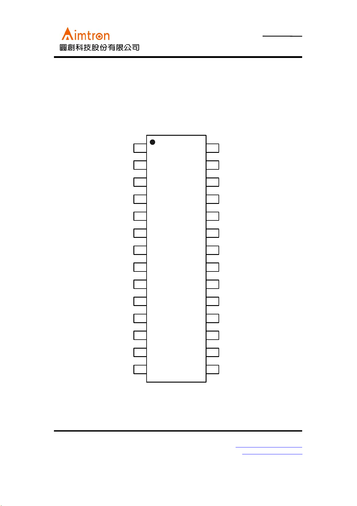
Pin Configuration
AT2101 (28-Pin 300 mil SOP)
DGND
D0
D1
D2
D3
D4
D5
D6
D7
D8
D9
1
2
3
4
5
6
7
8
9
10
11
28
27
26
25
24
23
22
21
20
19
18
NC
VIN
VCM
NC
AVDD
AVDD
NC
NC
AGND
AGND
NC
CLK
D10
D11 /OE
2F, No.10, Prosperity RD. II, Science-Based Industrial Park, Hsinchu 300,Taiwan, R.O.C.
Tel: 886-3-563-0878 WWW: http://www.aimtron.com.tw
Fax: 886-3-563-0879 Email: service@aimtron.com.tw
12
13
14
2
17
16
15
NC
DVDD
Page 3
AT2101
12-Bit 6MSPS A/D CONVERTER
Pin Description
PIN NAME FUNCTION PIN NAME FUNCTION
16 DV
DD
Digital +5V Supply 2324AV
DD
Analog +5V Supply
1 DGND Digital GND 1920AGND Analog GND
2~11 D0~D9
Digital Output Data
D0 (LSB) ~D9
13
14
D10
D11
Digital Output Data
D11 (MSB)
Output Enable Control
15 OE
D0~D11 Output Enabled
When OE = Low
26 VCM Common-Mode Voltage
Output
D0~D11 at High Impedance
When OE= High
12 CLK Clock Input 27 VIN Analog Input
17,18
21,22
NC
25,28
Absolute Maximum Ratings (Beyond which damage may occur) 250C
Supply Voltages
…………………………………………...-0.5 to +7.0 V
V
DD
Input Voltages
Analog Input ………………………………...AGND to V
Reference Input Voltage …………………...AGND to V
ESD Susceptibility ………………………………± 1,500V
DD
DD
2F, No.10, Prosperity RD. II, Science-Based Industrial Park, Hsinchu 300,Taiwan, R.O.C.
Tel: 886-3-563-0878 WWW: http://www.aimtron.com.tw
Fax: 886-3-563-0879 Email: service@aimtron.com.tw
Temperature
Operating Temperature …………..…………-20 to +70
Junction Temperature ………………………………175
Lead Temperature, (Soldering 10 seconds) ……..300
Storage Temperature …………………...…-55 to +125
3
0
C
0
C
0
C
0
C
Page 4

AT2101
12-Bit 6MSPS A/D CONVERTER
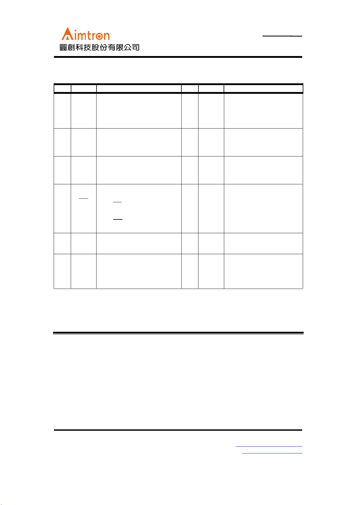
Electrical Specifications
Ta=+250C, AVDD=DVDD=+5.0V, AGND=DGND=0.0V, VRB=1V and VRT=3V, unless otherwise specified.
PARAMETERS TEST CONDICTION MIN TYP MAX UNITS
Resolution
DC Accuracy (+250C)
Integral Nonlinearity
Differential Nonlinearity
No Missing Codes
Zero Error(+25
Gain Error(+25
0
C)
0
C)
Analog Input
Input Voltage Range
Common-Mode Voltage
Input Bias Current
Sample-Hold Input Bandwidth
Input Resistance
Input Capacitance
Dynamic Performance
Signal-to-Noise Ratio
fin=500KHz
fin=1MHz
Spurious Free Dynamic Range
fin=500KHz
fin=1MHz
Timing Characteristics
Output Data Delay (td)
Output Data Delay (tdsl)
Data Valid Time
Sampling Time Offset
Digital Inputs
Input Current, Logic High
Input Current, Logic Low
Pulse Width High (CLK)
Pulse Width Low (CLK)
Voltage, Logic High
Voltage, Logic Low
Digital Outputs
Output Current, Logic High
Output Current, Logic Low
Voltage, Logic High
Voltage, Logic Low
Power Supply Requirements
AV
DV
(Analog Supply Voltage)
DD
(Digital Supply Voltage)
DD
Supply Voltage Difference
Supply Current
Power Dissipation
-3dBFS
Referred to Full Scale
Referred to Full Scale
(High ‘Z’)
Tri-state circuit
=5.25V, VIH=V
V
DD
VDD=5.25V, VIL=DGND
=min VOH=4.25V
V
DD
V
=min VOL=0.4V
DD
(AV
-DVDD)
DD
fs=6MSPS
12 Bits
± 1.5
± 0.5
Guaranteed
± 7.5
± 1.25
1.5 3.5
2.5
5
100
50
10
59
54
68
58 66
18 30
100
5 10
DD
10
83
83
4.0
1.0
-1.1
3.7
4.0
0.4
+4.75 +5.0 +5.25
+4.75 +5.0 +5.25
-0.1 0.0 0.1
65
325
100
100
LSB
LSB
%FSR
%FSR
V
V
µA
MHz
KΩ
pF
dB
dB
dB
dB
ns
ns
ns
ns
μA
μA
ns
ns
V
V
mA
mA
V
V
V
V
V
mA
mW
2F, No.10, Prosperity RD. II, Science-Based Industrial Park, Hsinchu 300,Taiwan, R.O.C.
Tel: 886-3-563-0878 WWW: http://www.aimtron.com.tw
Fax: 886-3-563-0879 Email: service@aimtron.com.tw
4
Page 5

AT2101
12-Bit 6MSPS A/D CONVERTER
Timing Specifications
Operating characteristic at VDD=5V, VRT=3.0V, VRB=1.0V, f
PARAMETERS TEST CONDICTION MIN TYP MAX UNITS
f
Maximum conversion rate 6 MSPS
CONV
td Sampling delay time 4 ns
tAJ Aperture jitter time 30 ps
tw(H) Clock pulse High 83 ns
tw(L) Clock Pulse Low 83 ns
t1 Data Hold time CL=10pF 15 ns
t2 New Data delay time CL=10pF 20 ns
tw(H) tw(L)
=20MHz, TA=250C (unless otherwise noted)
(CLK)
Clock
Analog
input
Data
Output
N
N-7
Data
Invalid
N+1
td
N-6
N+2
N+3
N+4
t2
N-5 N-4 N-3 N-2 N-1
N+5
t1
N+6
N+7
N
2F, No.10, Prosperity RD. II, Science-Based Industrial Park, Hsinchu 300,Taiwan, R.O.C.
Tel: 886-3-563-0878 WWW: http://www.aimtron.com.tw
Fax: 886-3-563-0879 Email: service@aimtron.com.tw
5
Page 6

AT2101
12-Bit 6MSPS A/D CONVERTER
Typical Application Schematic
+5V
+5V
15
16
17
18
19
20
21
22
23
24
25
14
13
12
11
10
9
8
7
6
5
4
D11 (MSB)
D10
Clock
Input
D9
D8
D7
D6
D5
D4
D3
(MSB)
D2
26
27
3
2
D1
D0
Analog
Input
2F, No.10, Prosperity RD. II, Science-Based Industrial Park, Hsinchu 300,Taiwan, R.O.C.
Tel: 886-3-563-0878 WWW: http://www.aimtron.com.tw
Fax: 886-3-563-0879 Email: service@aimtron.com.tw
28
6
1
Page 7

AT2101
12-Bit 6MSPS A/D CONVERTER
Package Outline (28-pin 300 mil SSOP)
DIMENSIONS IN
DIMENSIONS IN INCHESSYMBOLS
MILLIMETERS
MIN NOM MAX MIN NOM MAX
A 2.36 2.49 2.64 0.093 0.098 0.104
A1 0.10 - 0.30 0.004 - 0.012
A2 - 2.34 - - 0.092 -
B 0.33 0.41 0.51 0.013 0.016 0.020
C 0.23 0.25 0.33 0.009 0.010 0.012
D 17.70 - 18.10 0.697 - 0.713
E 7.39 7.49 7.59 0.291 0.295 0.299
e - 1.27 - - 0.050 H 10.01 10.31 10.64 0.394 0.406 0.419
L 0.38 0.81 1.27 0.015 0.032 0.050
y0- 80-8
h 0.25 - 0.75 0.01 - 0.029
2F, No.10, Prosperity RD. II, Science-Based Industrial Park, Hsinchu 300,Taiwan, R.O.C.
Tel: 886-3-563-0878 WWW: http://www.aimtron.com.tw
Fax: 886-3-563-0879 Email: service@aimtron.com.tw
7
Page 8

AT2101
12-Bit 6MSPS A/D CONVERTER
Reflow Condition (IR/Convection or VPR Reflow)
Reference JEDEC Standard J-STD-020A
Classification Reflow Profiles
Convection or
IR/Convction
Average Heating Rate(180°C to peak) 5°C/second max. 10°C/second max.
Preheat Temperature(125±20°C)
Temperature maintained above 180°C
Time within 5°C of actual Peak
Temperature
Peak Temperature Range(Note 1)
Cooling Rate
Time 25°C to Peak Temperature
*1 The maximum peak temperatures for IR and VP reflow are depending on package dimensions.
120 seconds max.
10~150 seconds
10~20 seconds 60 seconds
219~225°C or
235~240°C
6°C /second max. 10°C/second max.
6 minutes max.
219~225°C or
235~240°C
Package Reflow Conditions
Pkg. Thickness ≥2.5mm
and all bags
Pkg. Thickness <2.5mm
and
Pkg. Volume ≥350 mm
Convection 219~225°C Convection 235~240°C
VPR 219~225°C VPR 235~240°C
IR/Convection 219~225°C IR/Convection 235~240°C
Pkg. Thickness <2.5mm
and
3
Pkg. Volume <350 mm
VPR
3
2F, No.10, Prosperity RD. II, Science-Based Industrial Park, Hsinchu 300,Taiwan, R.O.C.
Tel: 886-3-563-0878 WWW: http://www.aimtron.com.tw
Fax: 886-3-563-0879 Email: service@aimtron.com.tw
8
 Loading...