

Page 1
AT1382A
4-Channel DC-DC Converter for DSC
Features
• Low start-up power supply voltage :1.4V(CH4)
• Wide supply voltage range from 1.8V to 7V
(CH1~4)
• High speed operation is possible: Maximum
1 MHz
• Supports for up, flyback and up/down SEPIC
conversion (CH1~4)
• Totem-pole type output for MOSFET
• Built-in On/Off function
• Built-in Short-Circuit Protection.
Applications
• Digital Cameras
• CCD Imaging Devices
• Camcorders
General Description
The AT1382A is a 4-channel PWM DC/DC control
IC for low voltage applications with a soft start
function and short circuit detection function. This
IC is ideal for up conversion, down conversion,
and up/down conversion (using a step-up/stepdown SEPIC system with free input and output
settings). Four channels can be built in the
LQFP48 package, each channel be controlled, and
soft-start.
The AT1382A include one comparator to generate
low-battery warning outputs. It also contains a gain
block that can be used with an external P-channel
MOSFET to make a low-dropout linear regulator.
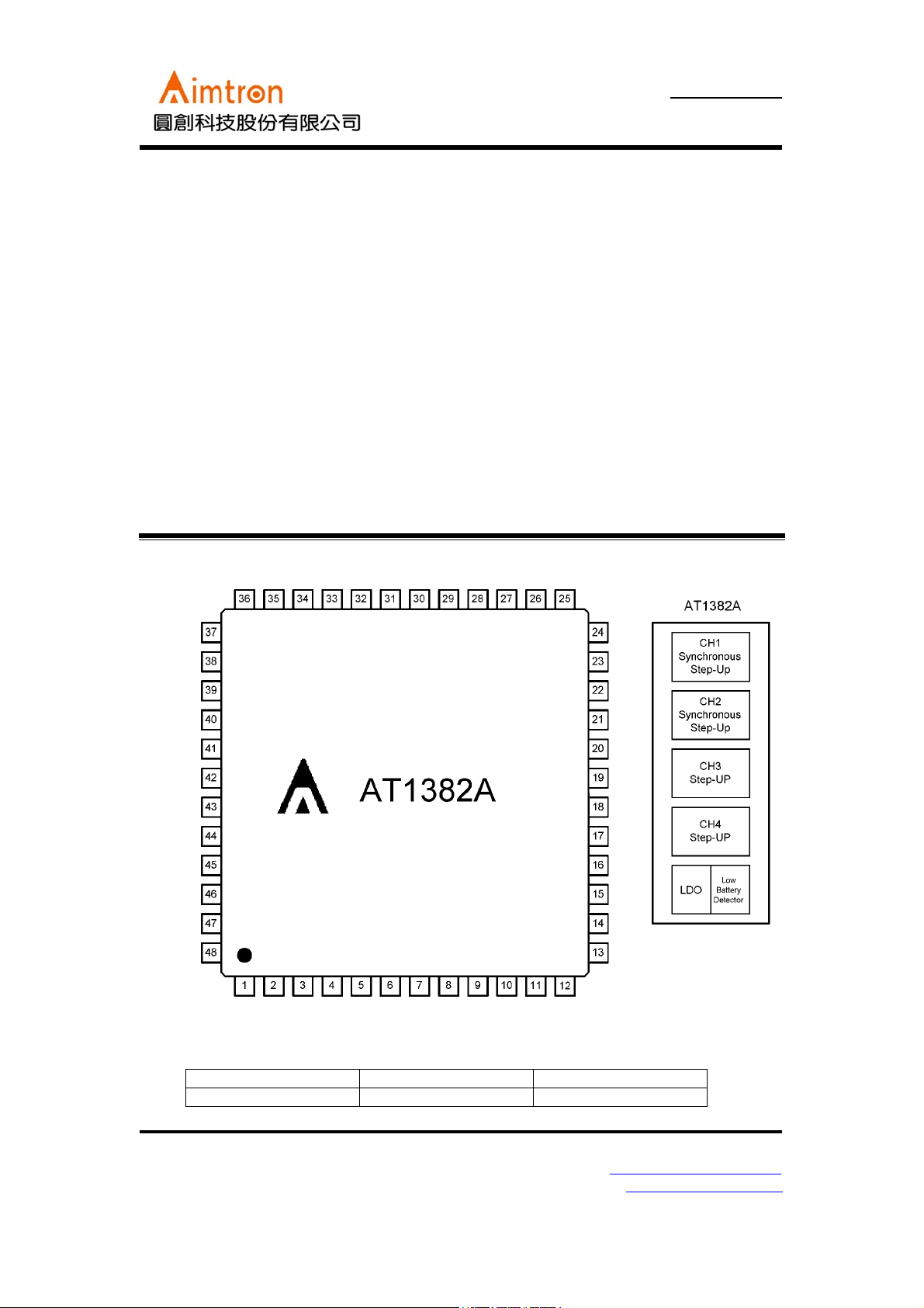
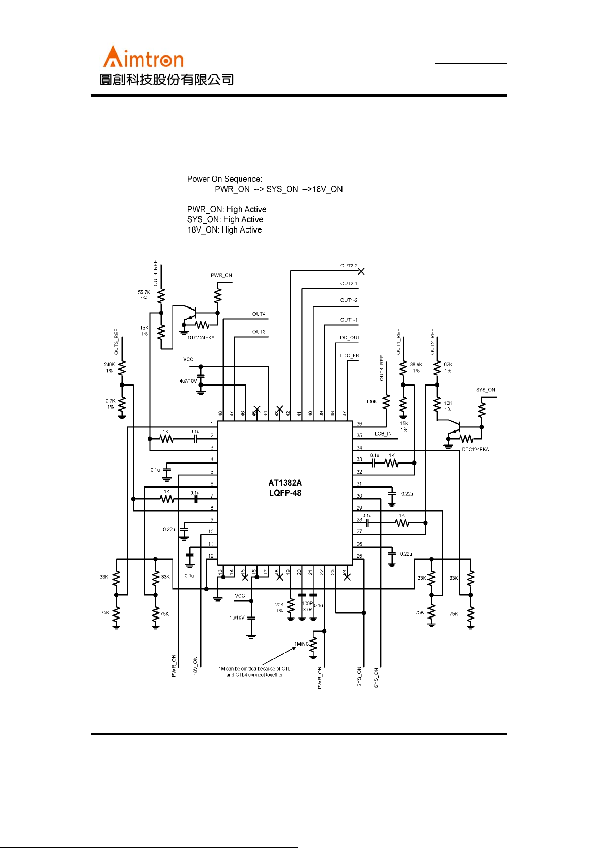
Pin Assignment
Ordering Information
Part number Package Marking
AT1382A LQFP48 AT1382AF
2F, No.10, Prosperity RD. II, Science-Based Industrial Park, Hsinchu 300,Taiwan, R.O.C.
Tel: 886-3-563-0878 WWW: http://www.aimtron.com.tw
Fax: 886-3-563-0879 Email: service@aimtron.com.tw
1
Page 2
AT1382A
4-Channel DC-DC Converter for DSC
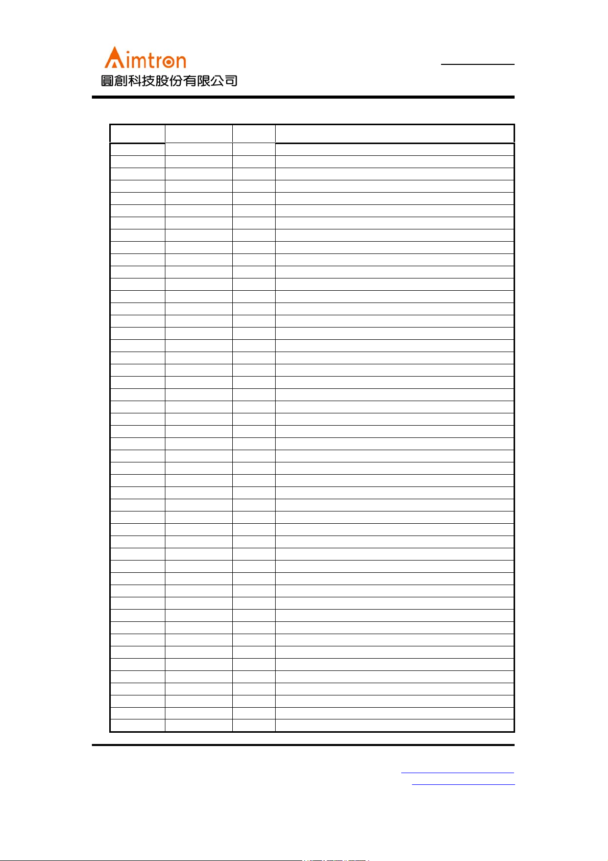
Pin Description
Pin No. Pin name I/O Function
1 DTC4 I CH4 Dead Time Control
2 FB4 O CH4 Error Amplifier Output
3 IN4 I CH4 Error Amplifier Inverted Input
4 CS4 - CH4 Soft Start Setting Capacitor
5 CTL4 I CH4 ON/OFF Control
6 DTC3 I CH3 Dead Time Control
7 FB3 O CH3 Error Amplifier Output
8 IN3 I CH3 Error Amplifier Inverted Input
9 CS3 - CH3 Soft Start Setting Capacitor
10 CTL3 I CH3 ON/OFF Control
11 CSCP - Timer Latch Short-Circuit Detection Capacitor Input
12 VREF O Reference 0.9V Output
13 GND P Ground
14 GND P Ground
15 VBG TEST Reference Test Pin
16 VCC P Power Supply
17 VCC P Power Supply
18 POR TEST Pre-OSC Change to Main-OSC Indicator
19 RT - Oscillation Frequency Setting Resistor
20 CT - Oscillation Frequency Setting Capacitor
21 VB O Reference 1.8V Output
22 CTL I Power Supply Control
23 ENLD I Gain Block Enable Input
24 CT2 TEST Triangular wave OSC Inverted output Test Pin
25 CTL2 I CH2 ON/OFF Control
26 CS2 - CH2 Soft Start Setting Capacitor
27 IN2 I CH2 Error Amplifier Inverted Input
28 FB2 O CH2 Error Amplifier Output
29 DTC2 I CH2 Dead Time Control
30 CTL1 I CH1 ON/OFF Control
31 CS1 - CH1 Soft Start Setting Capacitor
32 IN1 I CH1 Error Amplifier Inverted Input
33 FB1 O CH1 Error Amplifier Output
34 DTC1 I CH1 Dead Time Control
35 LBI I Low Battery Detected Input
36 LBO O Low Battery Indicator
37 AI I LDO Regulated Input
38 AO O LDO Drive Output
39 OUT1_1 O CH1 Main Side Output
40 OUT1_2 O CH1 Synchronous Rectifier Side Output
41 OUT2_1 O CH2 Main Side Output
42 OUT2_2 O CH2 Synchronous Rectifier Side Output
43 N.C. 44 PVCC P Drive Output Block Power Supply
45 N.C. 46 PGND P Drive Output Block Ground
47 OUT3 O CH3 Output
48 OUT4 O CH4 Output
2F, No.10, Prosperity RD. II, Science-Based Industrial Park, Hsinchu 300,Taiwan, R.O.C.
Tel: 886-3-563-0878 WWW: http://www.aimtron.com.tw
Fax: 886-3-563-0879 Email: service@aimtron.com.tw
2
Page 3
AT1382A
4-Channel DC-DC Converter for DSC
Block Diagram
2F, No.10, Prosperity RD. II, Science-Based Industrial Park, Hsinchu 300,Taiwan, R.O.C.
Tel: 886-3-563-0878 WWW: http://www.aimtron.com.tw
Fax: 886-3-563-0879 Email: service@aimtron.com.tw
3
Page 4
AT1382A
g
yp
4-Channel DC-DC Converter for DSC
Absolute Maximum Ratings
Parameter Symbol Condition
Ratin
Min Max
Unit
Power supply voltage Vcc -- -- 8 V
Output current Io Output pin -- 20 mA
Output peak current Io
Power dissipation P
Operation temperature Topr -- -30 85
Storage temperature Tstg -- -55 125
Semiconductor devices can be permanently damaged by application of stress in excess of absolute ratings. Do not
*
exceed these ratings.
Output pin, Duty≦5%
Ta≦25℃ (LQFP-48P)
D
-- 200 mA
-- 860 mW
℃
℃
Recommended Operating Conditions
Val ue
Parameter Symbol Condition
Min T
Startup power supply voltage Vcc CH4 1.4 -- 7 V
Power supply voltage Vcc
Reference voltage output current I
VB pin output current I
Input voltage V
Control input voltage V
Output current Io
Oscillator f
Timing capacitor C
Timing resistor R
Soft start capacitor
C
Short detection capacitor C
VB pin capacitor C
Operating ambient temperature Ta -- -30 25 85
CH4 1.5 5.0 7 V
CH1 to CH3 1.8 5.0 7 V
VREF pin -1 -- 0 mA
OR
VB pin -0.5 -- 0 mA
B
IN1 to IN4 pins 0 -- Vcc-1.8 V
IN
CTL pin 0 -- 7 V
CTL
OUT pin (CH1 to CH3) -- 2 15 mA
OUT pin (CH4) 1 2 15 mA
OSC
T
T
-- 100 500 1000 kHz
-- 47 100 560 pF
-- 8.2 18 100
Cs CH1 to CH3 -- 0.027 1.0
CH4 -- 0.47 1.0
+IN6
SCP
VB
-- -- 0.1 1.0
-- 0.082 0.1 --
Max
Unit
kΩ
μF
μF
μF
μF
℃
2F, No.10, Prosperity RD. II, Science-Based Industrial Park, Hsinchu 300,Taiwan, R.O.C.
Tel: 886-3-563-0878 WWW: http://www.aimtron.com.tw
Fax: 886-3-563-0879 Email: service@aimtron.com.tw
4
Page 5
AT1382A
4-Channel DC-DC Converter for DSC
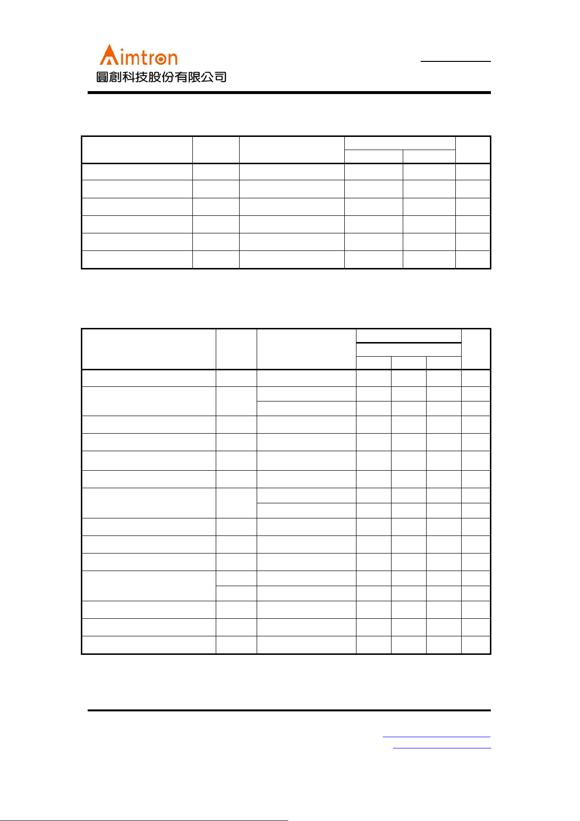
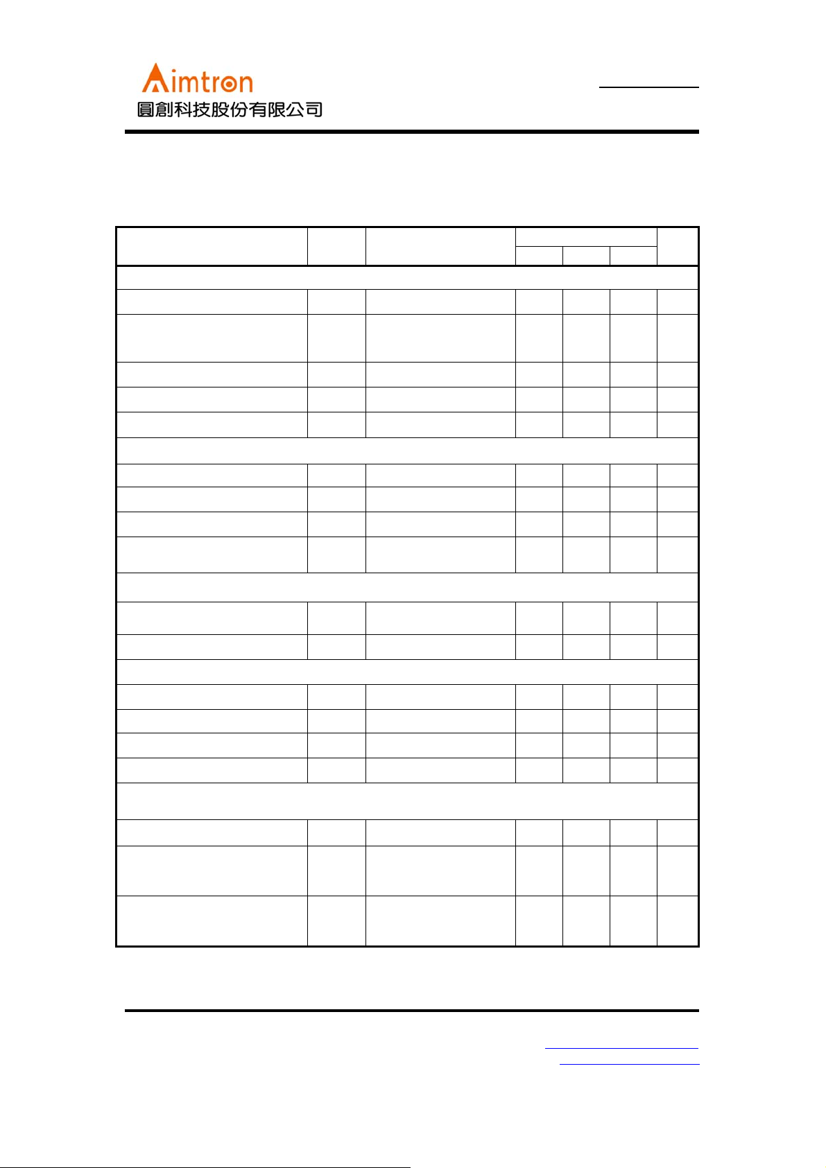
Electrical Characteristics
(Ta=25℃, VCC=PVCC=5V)
Parameter Symbol Condition
Reference voltage block [REF]
Measure result
Min. Typ. Max.
Unit
Reference voltage V
Output voltage temperature
△V
stability
/V
REF
REF
Ta = -30℃ to 85℃
REF
0.88 0.90 0.92 V
-0.5-%
Input stability Line VCC=1.8V to 7V -10 - 10 mV
Load stability Load VREF=0mA to –1mA -10 - 10 mV
Shout circuit output current I
VREF=0.7V -20 -5 -1 mA
OSC
Under voltage lockout block [U.V.L.O]
Threshold voltage(CH1~CH3) V
Hysteresis width(CH1~CH3) V
Reset voltage(CH1~CH3) V
CH4 Pre-OSC change to MainOSC threshold
V
TH
H
RST
TH2
1.5 1.6 1.7 V
-0.2-V
1.6 1.7 1.8 V
-1.7-V
Soft start block [CS]
Input standby voltage V
Charge current I
STB
CS
-50100mV
-6.0 -5.0 -4.0
μA
Short circuit detection block [SCP]
Threshold voltage V
Input standby voltage V
Input latch voltage V
Input source current I
TH
STB
I
CSCP
0.65 0.70 0.75 V
-50100mV
-50100mV
-1.4 -1.0 -0.6
μA
Triangular wave oscillator block [OSC]
Oscillator frequency f
Frequency stability for voltage
Frequency stability for
temperature
OSC
△f
/fdv
△f
/fdt
CT=100pF, RT=20kΩ
VCC=1.8V to 7V - 1 10 %
Ta=-30℃ to 85℃
450 500 550 kHz
-1-%
2F, No.10, Prosperity RD. II, Science-Based Industrial Park, Hsinchu 300,Taiwan, R.O.C.
Tel: 886-3-563-0878 WWW: http://www.aimtron.com.tw
Fax: 886-3-563-0879 Email: service@aimtron.com.tw
5
Page 6
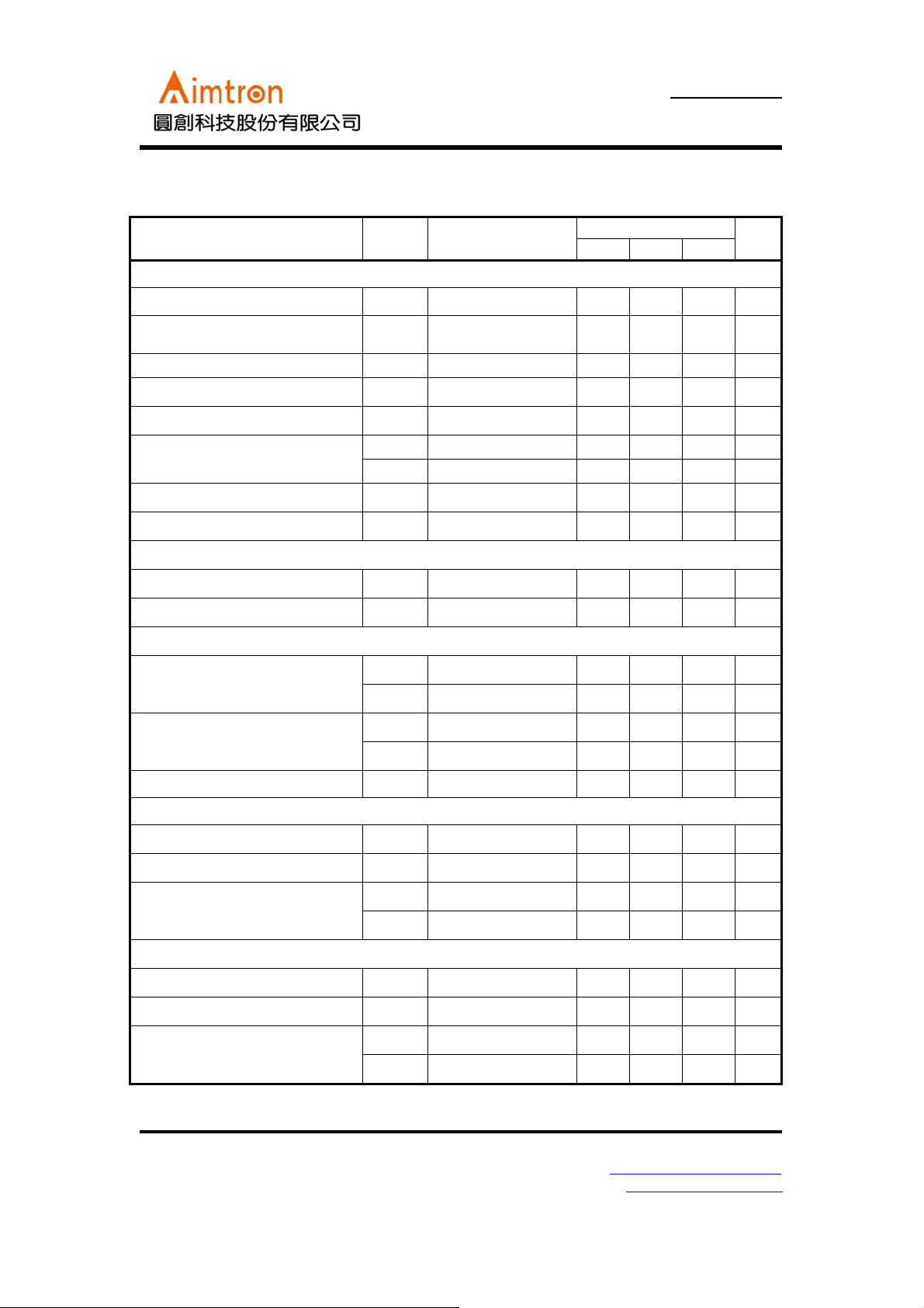
AT1382A
4-Channel DC-DC Converter for DSC
Parameter Symbol Condition
Measure result
Min. Typ. Max.
Unit
Error amplifier block [Error Amp](CH1~CH4)
Threshold voltage V
VT temperature stability
△V
Input bias current I
Voltage gain A
FB=0.9V 0.69 0.70 0.71 V
TH
Ta = -30℃ to 85℃
T/VT
IN=0V -320 -80 - nA
B
DC - 100 - dB
V
-0.5-%
Frequency bandwidth BW AV=0dB - 10 - MHz
Output voltage
Output source current I
Output sink current I
V
OH
V
OL
SOURCE
SINK
FB=0.5V - -4.0 -1.0 mA
FB=0.5V 70 140 -
1.3 1.4 - V
-50200mV
μA
Short detect comparator [SCP Comp]
Threshold voltage
Input bias current I
V
CH1 to CH4 0.65 0.7 0.75 V
TH
IN=0V -320 -80 - nA
B
PWM Comp. [PWM Comp]
V
Duty = 0 % 0.25 0.3 - V
Threshold voltage(CH4)
Threshold voltage(CH1~3)
Input current I
T0
V
V
Duty = 100 % - 0.75 0.80 V
Tmax
V
Duty = 0 % 0.20 0.25 -
T0
Duty = 100 % - 0.65 0.70
Tmax
DTC=0.4V -1.0 -0.3 -
DTC
μA
Output block (CH1,2) [Pin 39,41]
Output source current I
Output sink current I
Output ON resistor
SOURCE
SINK
R
OH
R
OL
Duty≧95%, OUT=0V
Duty≦5%, OUT=5V
OUT = -15mA - 18 30
OUT = 15mA - 16 25
- -130 -80 mA
65 100 - mA
Ω
Ω
Output block (CH1 to CH3) [Pin 40,42,47]
Output source current I
Output sink current I
Output ON resistor
SOURCE
SINK
R
OH
R
OL
Duty≧95%, OUT=0V
Duty≦5%, OUT=5V
OUT = -15mA - 18 30
OUT = 15mA - 16 25
- -130 -80 mA
65 100 - mA
Ω
Ω
2F, No.10, Prosperity RD. II, Science-Based Industrial Park, Hsinchu 300,Taiwan, R.O.C.
Tel: 886-3-563-0878 WWW: http://www.aimtron.com.tw
Fax: 886-3-563-0879 Email: service@aimtron.com.tw
6
Page 7
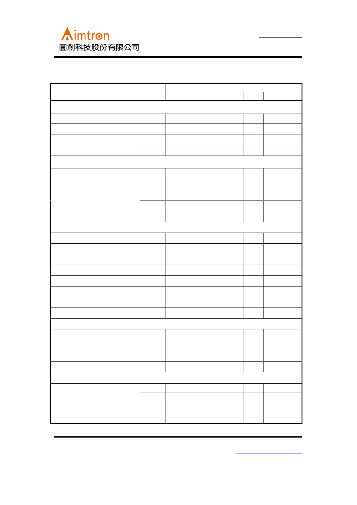
AT1382A
yp
4-Channel DC-DC Converter for DSC
Parameter Symbol Condition
Measure result
Min. T
Max.
Unit
Output block (CH4) [Pin 48]
Output source current I
Output sink current I
Output ON resistor
SOURCE
SINK
R
OH
R
OL
Duty≧95%, OUT=0V
Duty≦5%, OUT=5V
OUT = -15mA - 9 15
OUT = 15mA - 9 15
- -260 -160 mA
150 260 - mA
Ω
Ω
Control block [CTL]
V
Active mode 1.3 - 7 V
CTL input voltage
CTL1 to CTL4 input voltage
Input current I
IH
V
Standby mode 0 - 0.8 V
IL
V
Active mode 1.3 - 7 V
IH
V
Standby mode 0 - 0.8 V
IL
CTL = 5V - 5 20
CTL
μA
Analog gain block [AO,AI]
AI feedback regulation voltage VAO=V
-1.22V 1.20 1.22 1.24 V
OUT
AI input common-mode range -0.1 - 1.3 V
AI input current VAI=1.32V - - 100 nA
AI to AO voltage gain 70 100 140 V/V
AO output sink current VAI=1V, VAO=2V 0.5 2.5 - mA
AO output source current VAI=1.5V, VAO=2V 0.5 2.5 - mA
ENLD enable V
ENLD disable V
Active mode 1.2 - 7 V
IH
Standby mode 0 - 0.8 V
IL
Low battery detect block [LBI, LBO]
LBI detect threshold 1.20 1.22 1.24 V
Detect Hysteresis -50 +50 mV
LBO output voltage low Isink=1mA - - 0.4 V
LBO output high leakage
LBO
=5V
-0.011
μA
V
General
Standby current
Icss CTL=0V - - 10
Icss(o) CTL=0V - - 10
μA
μA
CTL=CTL1=CTL2=C
Power supply current Icc
TL3=CTL4=ENLD="
-36mA
H"
2F, No.10, Prosperity RD. II, Science-Based Industrial Park, Hsinchu 300,Taiwan, R.O.C.
Tel: 886-3-563-0878 WWW: http://www.aimtron.com.tw
Fax: 886-3-563-0879 Email: service@aimtron.com.tw
7
Page 8
AT1382A
4-Channel DC-DC Converter for DSC
Typical Application
A.
2F, No.10, Prosperity RD. II, Science-Based Industrial Park, Hsinchu 300,Taiwan, R.O.C.
Tel: 886-3-563-0878 WWW: http://www.aimtron.com.tw
Fax: 886-3-563-0879 Email: service@aimtron.com.tw
8
Page 9

AT1382A
4-Channel DC-DC Converter for DSC
2F, No.10, Prosperity RD. II, Science-Based Industrial Park, Hsinchu 300,Taiwan, R.O.C.
Tel: 886-3-563-0878 WWW: http://www.aimtron.com.tw
Fax: 886-3-563-0879 Email: service@aimtron.com.tw
9
Page 10

AT1382A
4-Channel DC-DC Converter for DSC
B. Using AT1382A on Buck Cnverter
2F, No.10, Prosperity RD. II, Science-Based Industrial Park, Hsinchu 300,Taiwan, R.O.C.
Tel: 886-3-563-0878 WWW: http://www.aimtron.com.tw
Fax: 886-3-563-0879 Email: service@aimtron.com.tw
10
Page 11

AT1382A
4-Channel DC-DC Converter for DSC
Function Description
1. Power Converter Functions
•Reference voltage block
The reference voltage circuit generates a temperature independence voltage (typical = 0.9V) from
the power source, which is used as reference voltage for the IC’s internal circuitry and supply load
current above 1mA to external device.
•Triangular oscillator block
The triangular wave oscillator is generated by timing resistor (RT) and timing capacitor(CT) to
incorporate each other. The waveforms CT (amplitude of 0.3V to 0.7V), CT1 (amplitude 0.25V
to 0.65V in phase with CT) and CT2 (amplitude 0.25V to 0.65V in inverse phase with CT) are
input to the PWM comparator.
•Error amplifier block
The error amplifier outputs controlling error signal to PWM comparator from sensing DC/DC
converter output voltage. In addition , an arbitrary loop gain can be set by connecting feedback
resistor and capacitor from the output pin to inverted input pin of the error amplifier, in order to
make a stable phase compensation to the system.
•PWM comparator block
The PWM comparator is a voltage-to-pulse width converter for controlling the duty cycle of
DC/DC converter.
Channels 1and 2 main sides, channel 3 and 4 : The comparator keeps the output transistor turn on
while the error amplifier output voltage and DTC voltage still higher than the triangular wave
voltage.
Channels 1 and 2 synchronous rectification sides : The comparator keeps the output transistor turn
on while the error amplifier output voltage still lower than the triangular wave voltage
•Output block
The output block is the totem pole configuration , which could drive external MOSFET or
transistor.
•Battery low detect block
The AT1382A battery-low comparator open-drain output LBO sinks up to 1mA if the LBI input is
below its threshold voltage. Connect LBO to power source with a 100K~1MΩ pullup resistor.
•Analog gain block
The AT1382A analog gain block is a voltage amplifier with a gain of 100 and a push-pull output
stage with 2mA drive capability. The analog gain block can be used with an external P-channel
MOSFET pass transistor to build a low-dropout linear regulator. Connect ENLD to High to enable
the gain block.
.
2F, No.10, Prosperity RD. II, Science-Based Industrial Park, Hsinchu 300,Taiwan, R.O.C.
Tel: 886-3-563-0878 WWW: http://www.aimtron.com.tw
Fax: 886-3-563-0879 Email: service@aimtron.com.tw
11
Page 12

AT1382A
4-Channel DC-DC Converter for DSC
2. Channel control function
The channels are turned on and turned off depending on the voltage levels at the CTL, CTL1,
CTL2, CTL3 and CTL4. Described as follow.
Voltage level at CTL pin Channel on / off state
CT L CLT1 C LT2 C LT3 CLT 4 CH 1 CH2 C H3 C H4
L X X X X OFF (Standby state)
L
H
H
X:Undefined
L
H
L
H
H
H
H
H
LOFFL
H
OFF
LOFF
H
LOFFL
H
OFF
ON
LOFF
H
LOFFL
H
OFF
LOFF
H
LOFFL
H
ON
ON
LOFF
H
OFF
ON
ON
ON
OFF
ON
ON
ON
OFF
ON
ON
ON
OFF
ON
ON
ON
3. Protective Functions
•Short circuit protection and timer latch
The short circuit detection comparator in each channel detects the output voltage level of power
converter. When any channel output voltage falls below the short-circuit detection level, there is a
constant current bias charging the external capacitor C
the capacitor voltage level reaches about 0.7V then turn off the output transistor and disable the IC.
It could reset the actuated protection by restart the power source.
•Under-voltage lockout protection
The under-voltage lockout protection is to disable the IC while the supply voltage transient state or
momentary decrease, which may cause the IC to malfunction. To prevent such malfunctions, the
under-voltage lockout protection circuit detects a decrease in internal reference voltage with
respect to the power supply voltage, turns off the output transistor, and sets the dead time to 100%
while holding the CSCP pin at the “L” level.
The circuit restores the output transistor to normal when the power source voltage reaches the
threshold voltage of the under-voltage lockout protection circuit.
2F, No.10, Prosperity RD. II, Science-Based Industrial Park, Hsinchu 300,Taiwan, R.O.C.
Tel: 886-3-563-0878 WWW: http://www.aimtron.com.tw
Fax: 886-3-563-0879 Email: service@aimtron.com.tw
12
which connected to the CSCP pin until
SCP
Page 13

AT1382A
4-Channel DC-DC Converter for DSC
Soft Start Operation
4.
When the CTL , CTL1, CTL2, CTL3 and CTL4 terminals are driven high level at the same time. The
driving scheme is described as follow diagram.
The capacitor connected to the CS1,CS2,CS3 and CS4 terminal starts charging and provides a soft
start by comparing the CH1 to CH4 output voltage .
2F, No.10, Prosperity RD. II, Science-Based Industrial Park, Hsinchu 300,Taiwan, R.O.C.
Tel: 886-3-563-0878 WWW: http://www.aimtron.com.tw
Fax: 886-3-563-0879 Email: service@aimtron.com.tw
13
Page 14

AT1382A
4-Channel DC-DC Converter for DSC
• When the CTL terminal is switch on, then each of the terminals CTL1, CTL2, CTL3, and CTL4
can be switched on or off independently. Any of the CTL1, CTL2, CTL3 and CTL4 terminals
are driven high level. The driving scheme is described as follow diagram.
2F, No.10, Prosperity RD. II, Science-Based Industrial Park, Hsinchu 300,Taiwan, R.O.C.
Tel: 886-3-563-0878 WWW: http://www.aimtron.com.tw
Fax: 886-3-563-0879 Email: service@aimtron.com.tw
14
Page 15

AT1382A
4-Channel DC-DC Converter for DSC
5. Soft start setting
The soft start operation is determined by the capacitor connected to the CS1~CS4 terminal.
Consider the input voltage and load current to design the soft start time.
The soft start time until the DC/DC converter output voltage reaches 95%. It can calculate the soft
start time Ts (s).
Ts (s) = 0.084 * C
(μF)
S
Ts
−
)(
×
CsR
eV
CS
= KR
The soft start function of CH1 to CH4 are the same. It could be disabled soft start function by
floating CS pin.
−×=
×
6.1176.33
6.1176.33
+
)1(7.0
Ω
6. Setting the output voltage
2F, No.10, Prosperity RD. II, Science-Based Industrial Park, Hsinchu 300,Taiwan, R.O.C.
Tel: 886-3-563-0878 WWW: http://www.aimtron.com.tw
Fax: 886-3-563-0879 Email: service@aimtron.com.tw
15
Page 16

AT1382A
4-Channel DC-DC Converter for DSC
7. Setting time constant for Time-latch Short-circuit protection
The SCP comparator detects each channel output voltage while the power converter work at
normal condition. Q1 is turn on, and the voltage level of CSCP pin is held at low level. If the load
of one channel rapidly due to a short of the load, causing the output voltage to drop, the SCP
comparator output on that channel goes to "H" level. The transistor Q1 to be turned off and the
external capacitor C
below equation.
t
(s): Short detection time
PE
to be charged at 1.0μA. The time period of short circuit protection as show
SCP
When the C
(s) = 0.7 * C
t
PE
is charged to the 0.7V, the timer-latch is set and output is turn off (dead time is set to 100
SCP
SCP
(μF)
﹪). At this point, the timer-latch is closed and the CSCP terminal is held at "L" level. It could be
disabled short circuit protection function by connecting CSCP pin into the ground.
2F, No.10, Prosperity RD. II, Science-Based Industrial Park, Hsinchu 300,Taiwan, R.O.C.
Tel: 886-3-563-0878 WWW: http://www.aimtron.com.tw
Fax: 886-3-563-0879 Email: service@aimtron.com.tw
16
Page 17

AT1382A
﹪
4-Channel DC-DC Converter for DSC
8. Setting the triangular oscillator frequency
The triangular oscillator frequency is determined by the timing capacitor (CT) connected to the CT
terminal, and the timing resistor (R
) connected to the RT terminal.
T
1000000
)()(
Ω×
kRPFC
TT
OSC
)(
=
kHzf
9. Setting the DEAD time
When using step up or SEPIC or flyback DC/DC converter, it must prevent that output transistor
works at full-ON state (ON duty = 100%). To prevent this situation, set the maximum duty of these
channels. To set it, set the voltage at the DTC terminal by applying a resistive voltage divider to
the VREF as shown below.
When the voltage at the DTC pin is higher than the triangular wave voltage (CT), the output
transistor is turned on. The maximum duty calculation formula assuming that triangular wave
amplitude = ∆V1(CH4=0.45,CH1~3=0.4) and triangular wave minimum voltage = Vx
(CH4=0.3,CH1~3=0.25).
−
VxVd
max)( ×
ONDUTY
If don't setting maximum duty, connect DTC terminal directly to the VREF terminal.
=
V
∆
100
1
2F, No.10, Prosperity RD. II, Science-Based Industrial Park, Hsinchu 300,Taiwan, R.O.C.
Tel: 886-3-563-0878 WWW: http://www.aimtron.com.tw
Fax: 886-3-563-0879 Email: service@aimtron.com.tw
17
Page 18

AT1382A
4-Channel DC-DC Converter for DSC
10. Setting low battery detector threshold voltage
The low battery detected threshold voltage is determined by the external resistor connected to the
LBI terminal. If Vin (battery voltage) under setting threshold voltage, low battery detect output
terminal (LBO) is hold at "L" level. The driving scheme is described as follow diagram.
11. Decrease the Output Overshoot
2F, No.10, Prosperity RD. II, Science-Based Industrial Park, Hsinchu 300,Taiwan, R.O.C.
Tel: 886-3-563-0878 WWW: http://www.aimtron.com.tw
Fax: 886-3-563-0879 Email: service@aimtron.com.tw
18
Page 19

AT1382A
4-Channel DC-DC Converter for DSC
Synchronous Rectification Reference Data
2F, No.10, Prosperity RD. II, Science-Based Industrial Park, Hsinchu 300,Taiwan, R.O.C.
Tel: 886-3-563-0878 WWW: http://www.aimtron.com.tw
Fax: 886-3-563-0879 Email: service@aimtron.com.tw
19
Page 20

AT1382A
4-Channel DC-DC Converter for DSC
2F, No.10, Prosperity RD. II, Science-Based Industrial Park, Hsinchu 300,Taiwan, R.O.C.
Tel: 886-3-563-0878 WWW: http://www.aimtron.com.tw
Fax: 886-3-563-0879 Email: service@aimtron.com.tw
20
Page 21

AT1382A
4-Channel DC-DC Converter for DSC
*if VCC=PVCC=3.3V, the efficiency will decrease about 0.2~05 % because of the N-
MOSFET AO3400 Rds(on) increase.
2F, No.10, Prosperity RD. II, Science-Based Industrial Park, Hsinchu 300,Taiwan, R.O.C.
Tel: 886-3-563-0878 WWW: http://www.aimtron.com.tw
Fax: 886-3-563-0879 Email: service@aimtron.com.tw
21
Page 22

AT1382A
4-Channel DC-DC Converter for DSC
Typical Characteristics
2F, No.10, Prosperity RD. II, Science-Based Industrial Park, Hsinchu 300,Taiwan, R.O.C.
Tel: 886-3-563-0878 WWW: http://www.aimtron.com.tw
Fax: 886-3-563-0879 Email: service@aimtron.com.tw
22
Page 23

AT1382A
4-Channel DC-DC Converter for DSC
2F, No.10, Prosperity RD. II, Science-Based Industrial Park, Hsinchu 300,Taiwan, R.O.C.
Tel: 886-3-563-0878 WWW: http://www.aimtron.com.tw
Fax: 886-3-563-0879 Email: service@aimtron.com.tw
23
Page 24

AT1382A
4-Channel DC-DC Converter for DSC
Typical Characteristics
LQFP48
2F, No.10, Prosperity RD. II, Science-Based Industrial Park, Hsinchu 300,Taiwan, R.O.C.
Tel: 886-3-563-0878 WWW: http://www.aimtron.com.tw
Fax: 886-3-563-0879 Email: service@aimtron.com.tw
24
Page 25

AT1382A
C
4-Channel DC-DC Converter for DSC
Reflow Condition (IR/Convection or VPR Reflow)
Reference JEDEC Standard J-STD-020A
Classification Reflow Profiles
Convection or
IR/Convction
Average Heating Rate(180°C to peak) 5°C/second max. 10°C/second max.
Preheat Temperature(125±20°C)
Temperature maintained above 180°C
Time within 5°C of actual Peak
Temperature
Peak Temperature Range(Note 1)
Cooling Rate
Time 25°C to Peak Temperature
*1 The maximum peak temperatures for IR and VP reflow are depending on package dimensions.
120 seconds max.
10~150 seconds
10~20 seconds 60 seconds
219~225°C or
235~240°C
6°C /second max. 10°C/second max.
6 minutes max.
219~225°C or
235~240°C
Package Reflow Conditions
Pkg. Thickness ≥2.5mm
and all bags
Convection 219~225
VPR 219~225
°C
IR/Convection 219~225
°C
°C
Pkg. Thickness <2.5mm
and
Pkg. Volume ≥350 mm
Pkg. Thickness <2.5mm
and
3
Pkg. Volume <350 mm
Convection 235~240
VPR 235~240
IR/Convection 235~240
VPR
3
°C
°C
°
2F, No.10, Prosperity RD. II, Science-Based Industrial Park, Hsinchu 300,Taiwan, R.O.C.
Tel: 886-3-563-0878 WWW: http://www.aimtron.com.tw
Fax: 886-3-563-0879 Email: service@aimtron.com.tw
25
 Loading...