

Page 1
AT1380A
Switching Regulator Controller for LCD Bias
Features
•2.5 to 15 V supply voltage operating range.
•Low current consumption: 6 mA in operation,
1 µA or less in stand-by.
•20 kHz to 1 MHz operation frequency range.
•Provides a fixed output current with minimal
supply voltage fluctuations by using an external
resistor to set the output current.
• Totem-pole output.
• Built-in soft start circuit.
• Built-in timer-latch short circuit detection and
protection circuit (SCP).
Applications
• LCD Displays
• PDAs
• Digital Still Cameras
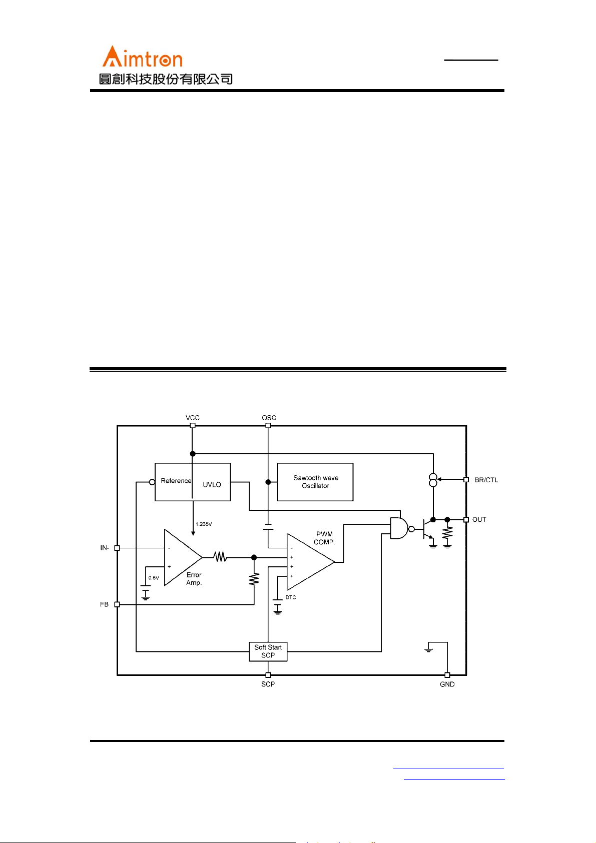
Block Diagram
General Description
The AT1380A is a single-channel PWM control IC
for DC/DC conversion with soft start function and
short circuit detection. Adjustable soft start is
programmed with an external capacitor on SCP
pin. The AT1380A is ideal for up, down and flyback conversion.
2F, No.10, Prosperity RD. II, Science-Based Industrial Park, Hsinchu 300,Taiwan, R.O.C.
Tel: 886-3-563-0878 WWW: http://www.aimtron.com.tw
Fax: 886-3-563-0879 Email: service@aimtron.com.tw
1
Page 2
AT1380A
Switching Regulator Controller for LCD Bias
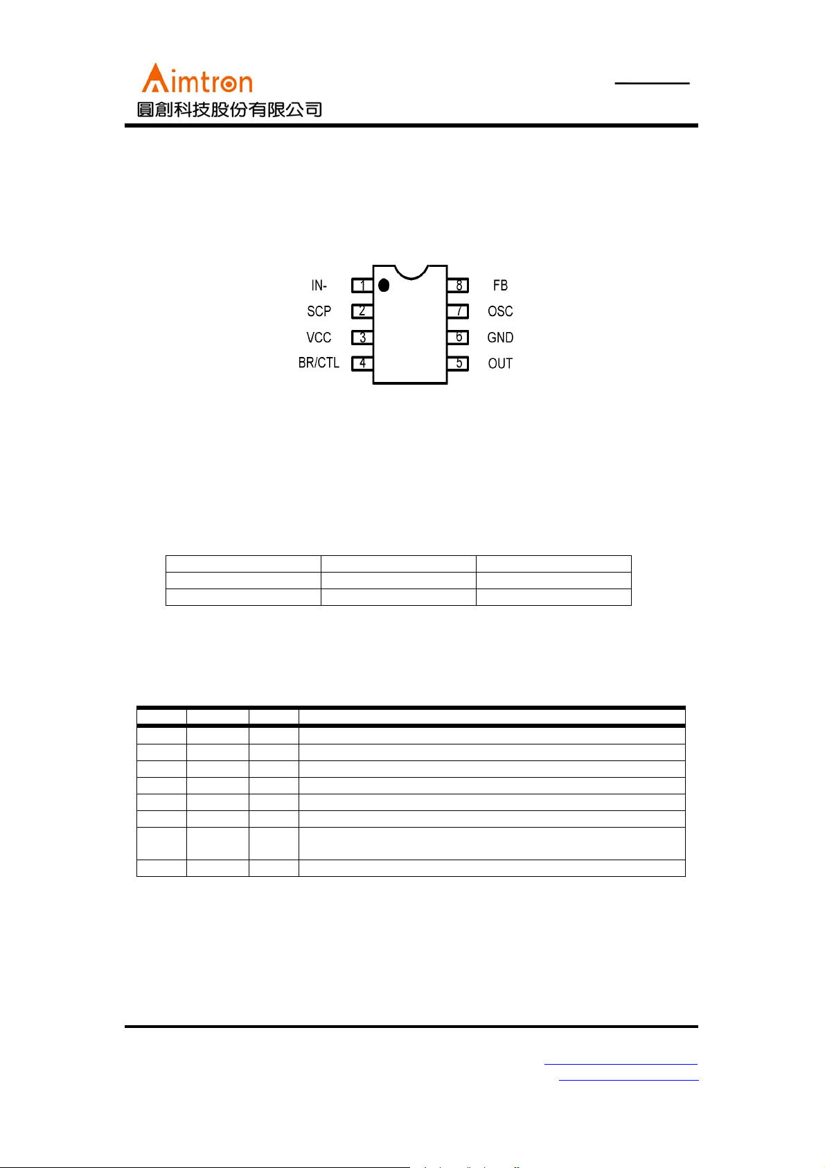
Pin Configuration
Ordering Information
Part number Package Remarks
AT1380A 8-pin Plastic SOP AT1380AS
AT1380A 8-pin TSSOP AT1380AP
Pin Description
Pin No. Symbol I/O Description
1 IN- I Error amplifier inverting input
2 SCP — Soft start and SCP setting capacitor connection
3 VCC — Power supply
4 BR/CTL I Output current setting
5 OUT O Totem-pole type output
6GND—Ground
7 OSC — Capacitor and resistor connection pin for setting the oscillation
frequency
8 FB O Error amplifier output
2F, No.10, Prosperity RD. II, Science-Based Industrial Park, Hsinchu 300,Taiwan, R.O.C.
Tel: 886-3-563-0878 WWW: http://www.aimtron.com.tw
Fax: 886-3-563-0879 Email: service@aimtron.com.tw
2
Page 3
AT1380A
Switching Regulator Controller for LCD Bias
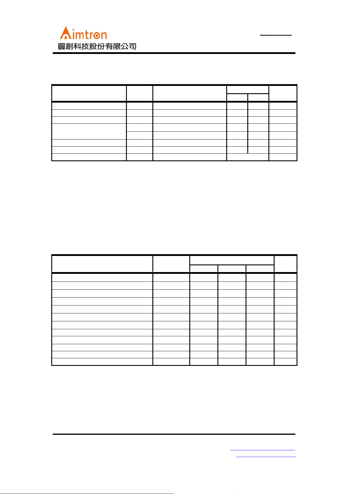
Absolute Maximum Ratings
(Ta=+250C)
Rated ValueParameter Symbol Condition
Unit
Min. Max.
Power supply voltage V
Output source current I
Output sink current I
Allowable dissipation
Operating temperature T
Storage temperature T
CC
+
O
-
O
P
D
P
D
OP
stg
SOP-8, Ta ≦+25°C
TSSOP-8, Ta ≦+25°C
——15V
——-50mA
——50mA
—570 mW
—430 mW
—-30+85
— -55 +125
0
C
0
C
ESD Classification MIL-STD-883 Class 2
* : When mounted on a 10 cm square double-sided epoxy board
WA R N IN G : Do not exceed these ratings. IC devices can be permanently damaged by stress (voltage,
current, temperature, etc.) in excess of absolute maximum ratings.
Recommended Operating Conditions
(Ta=+250C)
Va lu esParameter Symbol
Min. Typ. Max.
Power supply voltage V
Error amplifier input voltage V
BR/CTL pin input voltage V
Output source current I
Output sink current I
SCP pin capacitance C
Phase compensation capacitance C
Output current setting resistance R
Timing resistance R
Timing capacitance C
Oscillation frequency f
Operating temperature T
O
O
OSC
OP
CC
BR
PE
I
+
-
P
B
T
T
2.5 -- 13.5
-0.2 -- 1.0
-0.2 -- V
CC
-20 -- --
-- -- 40
-- 0.1 --
-- 0.1 --
150 390 5000 Ω
1.0 3.0 10.0
100 270 10000 pF
10 500 1000 kHz
-30 +25 +85 °C
WA R N IN G : Recommended operating conditions are normal operating ranges for the IC device. All
the device’s electrical characteristics are warranted for operation within these ranges. Use IC devices
only within the recommended operating conditions. Operation outside these ranges may adversely
affect the reliability and can result in device failure.
Unit
V
V
V
mA
mA
μF
μF
kΩ
2F, No.10, Prosperity RD. II, Science-Based Industrial Park, Hsinchu 300,Taiwan, R.O.C.
Tel: 886-3-563-0878 WWW: http://www.aimtron.com.tw
Fax: 886-3-563-0879 Email: service@aimtron.com.tw
3
Page 4
AT1380A
Switching Regulator Controller for LCD Bias
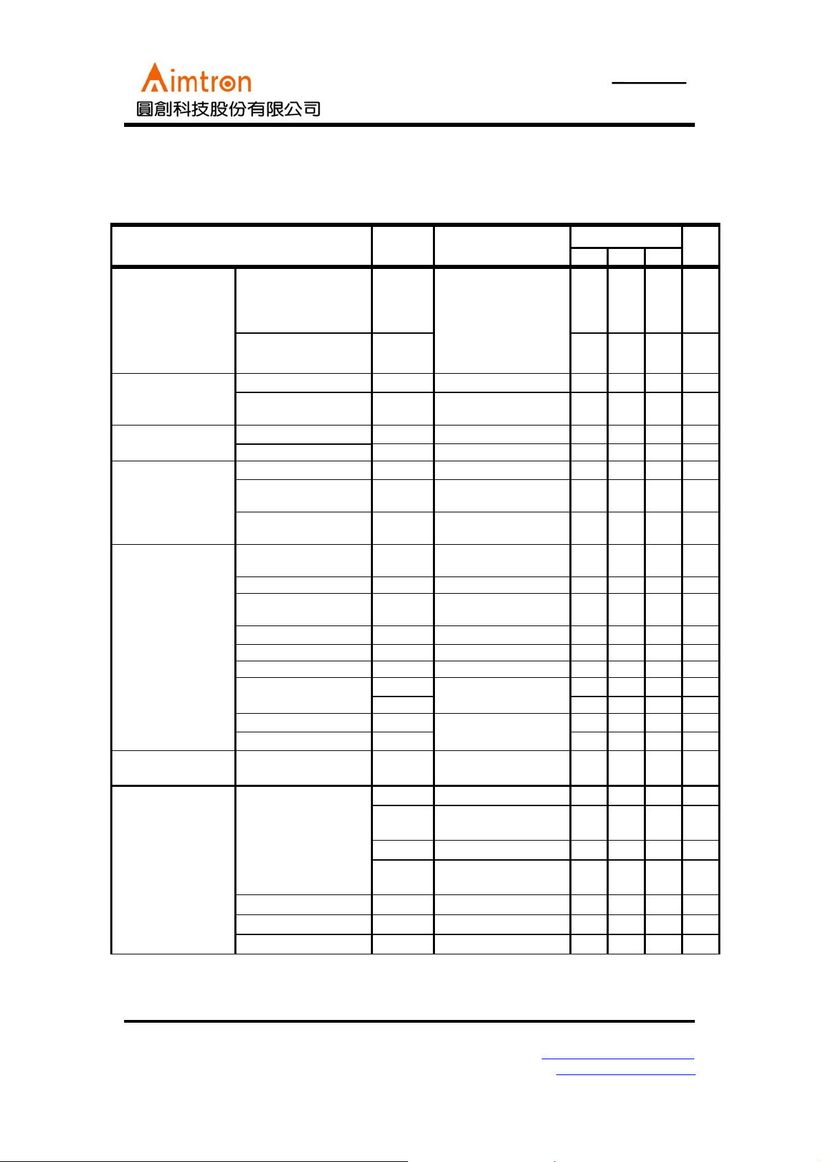
Electrical Characteristics
(VCC=+3.0V, Ta=+250C)
Va lu esParameter Symbol Condition
Min. Typ. Max.
Lockout
(U.V.L.O.)
Reset voltage for
falling Vcc. OUT
remains off if Vcc is
below this level.
Startup voltage for
rising Vcc.
V
R
-- 1.8 1.9 VVCC Under voltage
--
V
TH
2.4 2.5 2.6 V
Unit
Soft start
Short circuit
detection (S.C.P.)
Sawtooth waveform
oscillator (OSC)
Error amplifier
Idle period
adjustment section
Output section
Charging current I
Voltage at soft start
V
CS
V
ts
=0V -1.5 -1.0 -0.7
SCP
-- 0.7 0.8 0.9 V
μA
completion
Charging current I
Threshold voltage V
Oscillation frequency f
Frequency input
V
CPC
OSC
f
tPC
∆V
=0V -1.5 -1.0 -0.7
SCP
-- 0.7 0.8 0.9 V
RT=3kΩ, CT=270pF
400 500 600 kHz
VCC=2.5V to 13.5V -- 2 10 %
μA
Stability
Frequency variation
f
Ta =-300C to 850C--5--%
∆T
with temperature
Input threshold
V
V
T
= 450mV 480 500 520 mV
FB
Voltage
VT input stability V
VT variation with
V
VCC=2V to 13.5V -- 5 20 mV
T∆V
Ta = -300C to 850C--1--%
T∆T
Temperature
Input bias current I
Voltage gain A
Frequency bandwidth BW AV = 0 dB -- 6 -- MHz
V
voltage range
V
Output source current I
Output sink current I
Maximum duty cycle T
V
V
Output voltage
V
V
Output source current I
Output sink current I
Pull down resistance R
VIN = 0V -1.0 -0.2 1.0
B
V
+
OM
_
OM
+
V
OM
OM
DUTY
OH1
OH2
OL1
OL2
O
O
FB
_
RT=3.3kΩ, CT=270pF
f
OSC
RB= 390Ω, IO= -15 mA
RB= 750Ω, VCC = 3.0V
= -10 mA
I
O
RB= 390Ω, IO= -15 mA
RB= 750Ω, VCC = 3.0V
= -10 mA
I
O
+
RB= 390Ω, VO = 0.9V
-
RB= 390Ω, VO = 0.3V
O
-- 70 100 145 V/V
--
0.78 0.87 -- VMaximum output
= 450mV
= 500KHz
-- 20 30 40
μA
-- 0.05 0.2 V
-- -40 -24
24 40 --
μA
μA
75 -- 85 %
1.0 1.2 -- V
0.8 1.0 -- V
-- 0.1 0.2 V
-- 0.1 0.2 V
-- -40 -30 mA
40 70 -- mA
kΩ
2F, No.10, Prosperity RD. II, Science-Based Industrial Park, Hsinchu 300,Taiwan, R.O.C.
Tel: 886-3-563-0878 WWW: http://www.aimtron.com.tw
Fax: 886-3-563-0879 Email: service@aimtron.com.tw
4
Page 5

AT1380A
Switching Regulator Controller for LCD Bias
0.10 0.19 0.25 V
-20 -- 0
-- -- -45
-1.8 -- -0.1
-- -- 1
-- 6 10.0
Output current
Setting section/
Control section
Entire device
Pin voltage V
Input off condition I
Input on condition I
Pin current range I
Stand-by current I
Average supply current I
RB= 390Ω
BR
OFF
ON
BR
BR/CTL pin open or
CCS
V
CC
RB= 390,
CC
=2.5~13.5V
V
CC
--
Timing Chart
μA
μA
mA
μA
mA
2F, No.10, Prosperity RD. II, Science-Based Industrial Park, Hsinchu 300,Taiwan, R.O.C.
Tel: 886-3-563-0878 WWW: http://www.aimtron.com.tw
Fax: 886-3-563-0879 Email: service@aimtron.com.tw
5
Page 6

AT1380A
Switching Regulator Controller for LCD Bias
Typical Application Schematic
2F, No.10, Prosperity RD. II, Science-Based Industrial Park, Hsinchu 300,Taiwan, R.O.C.
Tel: 886-3-563-0878 WWW: http://www.aimtron.com.tw
Fax: 886-3-563-0879 Email: service@aimtron.com.tw
6
Page 7

AT1380A
Switching Regulator Controller for LCD Bias
2F, No.10, Prosperity RD. II, Science-Based Industrial Park, Hsinchu 300,Taiwan, R.O.C.
Tel: 886-3-563-0878 WWW: http://www.aimtron.com.tw
Fax: 886-3-563-0879 Email: service@aimtron.com.tw
7
Page 8

AT1380A
Switching Regulator Controller for LCD Bias
Functional Description
Soft Start SCP
Figure 1. Soft-Start SCP circuit
At power-on, the AT1380A enters the soft-start mode to prevent current spike and overshoot. The
capacitor CS is charged from 0V at a constant current of 1µA.
The soft-start time for the duty cycle to reach 50%
)(35.0 FCSt
µ
S
When V
the SCP function. If the output load conditions change rapidly causing the output to drop suddenly, the
external capacitor CS will start to charge because the error amplifier output (FB pin) is fixed at V
When the external capacitor is charged above 0.8V, the output pin is set low. Once the latch circuit has
set, the capacitor CS will be discharged to low state and the latch circuit will not reset until power is
turned off or the power supply is restarted.
Short-circuit detection time (or full soft-start time) :
reaches 0.8V, the AT1380A leaves the soft-start mode to enter the normal mode and enable
SCP
PE
×=
OM
µ
×=
)(8.0 FCSt
.
+
2F, No.10, Prosperity RD. II, Science-Based Industrial Park, Hsinchu 300,Taiwan, R.O.C.
Tel: 886-3-563-0878 WWW: http://www.aimtron.com.tw
Fax: 886-3-563-0879 Email: service@aimtron.com.tw
8
Page 9

AT1380A
Switching Regulator Controller for LCD Bias
Setting Oscillating Frequency
The oscillator circuit generates a triangular sawtooth wave with a peak of 0.8V and a trough of 0.1V
using the timing capacitor (CT) and the timing resistor (RT) that are connected to the OSC pin. This
oscillator can provide oscillating frequency in the range from 20KHz to 1MHz. The waveform of the
OSC pin is shown as Figure 2.
Figure 2 Oscillator Waveform
The cycle (T) can be determined as follows:
t
−
RTCT
VHeVX
=
Switching Regulator Function
(1) Reference voltage circuit
A temperature-compensated reference voltage (~1.25V) is generated by the reference voltage
circuit from the voltage supplied by the power supply pin (pin 3). The circuit also sets the idle
period besides providing the reference voltage for the switching regulator.
(2) Error amplifier
The error amplifier detects the output voltage of the switching regulator and sets the PWM
control signal. The voltage gain is fixed. The system is made stable by connecting a phase
×
e
RTCTt
××−=
VX
)(log
e
VH
[]
sRTCTRTCTT
××=××−= 1.2)8.0/1.0(log
compensation capacitor to the FB pin (pin 8).
(3) PWM comparator
The voltage comparator includes one inverting and three non-inverting inputs. The comparator is
2F, No.10, Prosperity RD. II, Science-Based Industrial Park, Hsinchu 300,Taiwan, R.O.C.
Tel: 886-3-563-0878 WWW: http://www.aimtron.com.tw
Fax: 886-3-563-0879 Email: service@aimtron.com.tw
9
Page 10

AT1380A
Switching Regulator Controller for LCD Bias
a voltage to pulse width converter that controls the ON time of the output pulse depending on the
level of input voltage. The output level remains high when the sawtooth wave is lower than the
error amplifier output voltage, the soft start setting voltage, and the idle period setting voltage.
(4) Output circuit
The output circuit can drive an external NPN transistor directly and has a totem pole
configuration. The value of the ON/OFF current can be set by a resistor connected to the
BR/CTL pin (pin 4). Stand-by mode (supply current 1µA or less) can be set by connecting the
BR/CTL pin (pin4) to VCC or by making the pin open.
(5) Under-Voltage Lockout (UVLO)
Transients during powering on or instantaneous glitches in the supply voltage can cause the
control IC to malfunction and damage the system. To prevent malfunction at low input voltage,
the circuit compares the supply voltage to the internal reference voltage to detect a low input
voltage. Once detected, the circuit sets the output pin low.
To cancel the status, set V
recommended operation range and the latch will be restored to operate normally.
below the reset voltage VR (0.9V) and then set VCC up to the
CC
2F, No.10, Prosperity RD. II, Science-Based Industrial Park, Hsinchu 300,Taiwan, R.O.C.
Tel: 886-3-563-0878 WWW: http://www.aimtron.com.tw
Fax: 886-3-563-0879 Email: service@aimtron.com.tw
10
Page 11

AT1380A
Switching Regulator Controller for LCD Bias
Small Outline 8-pin Plastic SOL
SYMBOL
INCHES MILLIMETERS
MIN MAX MIN MAX
NOTES
A 0.188 0.197 4.80 5.00 B 0.149 0.158 3.80 4.00 C 0.228 0.244 5.80 6.20 D 0.050 BSC 1.27 BSC E 0.013 0.020 0.33 0.51 -
F 0.004 0.010 0.10 0.25 -
H 0.053 0.069 1.35 1.75 -
J 0.011 0.019 0.28 0.48
K 0.007 0.010 0.19 0.25 -
M 0.016 0.050 0.40 1.27
L 0.150 REF 3.81 REF -
e1 45
α
0
0
0
0
8
0
0
45
0
0
8
-
-
2F, No.10, Prosperity RD. II, Science-Based Industrial Park, Hsinchu 300,Taiwan, R.O.C.
Tel: 886-3-563-0878 WWW: http://www.aimtron.com.tw
Fax: 886-3-563-0879 Email: service@aimtron.com.tw
11
Page 12

AT1380A
Switching Regulator Controller for LCD Bias
Small Outline 8-pin TSSOP
SYMBOL
INCHES MILLIMETERS
MIN MAX MIN MAX
NOTES
A 0.114 0.122 2.90 3.10 B 0.169 0.177 4.30 4.50 C 0.244 0.260 6.20 6.60 D 0.026 BSC 0.65 BSC E 0.010 0.012 0.25 0.30 -
F 0.002 0.006 0.05 0.15 H 0.041 0.047 1.05 1.20 K 0.005 BSC 0.127 BSC -
M 0.020 0.028 0.50 0.70
α
0
0
0
8
0
0
0
8
-
2F, No.10, Prosperity RD. II, Science-Based Industrial Park, Hsinchu 300,Taiwan, R.O.C.
Tel: 886-3-563-0878 WWW: http://www.aimtron.com.tw
Fax: 886-3-563-0879 Email: service@aimtron.com.tw
12
Page 13

C
AT1380A
Switching Regulator Controller for LCD Bias
Reflow Condition (IR/Convection or VPR Reflow)
Reference JEDEC Standard J-STD-020A
Classification Reflow Profiles
Convection or
IR/Convction
Average Heating Rate(180°C to peak)
Preheat Temperature(125±20°C)
Temperature maintained above 180°C
Time within 5°C of actual Peak Temperature
Peak Temperature Range(Note 1)
Cooling Rate
Time 25°C to Peak Temperature
*1 The maximum peak temperatures for IR and VP reflow are depending on package dimensions.
5
°C/second max.
120 seconds max.
10~150 seconds
10~20 seconds 60 seconds
219~225°C or
235~240°C
6°C /second max. 10°C/second max.
6 minutes max.
Package Reflow Conditions
Pkg. Thickness ≥2.5mm
and all bags
Convection 219~225
VPR 219~225
°C
IR/Convection 219~225
°C
°C
Pkg. Thickness <2.5mm
and
Pkg. Volume ≥350 mm
Pkg. Thickness <2.5mm
and
3
Pkg. Volume <350 mm
Convection 235~240
VPR 235~240
IR/Convection 235~240
VPR
10
°C/second max.
219~225°C or
235~240°C
°C
3
°C
°
2F, No.10, Prosperity RD. II, Science-Based Industrial Park, Hsinchu 300,Taiwan, R.O.C.
Tel: 886-3-563-0878 WWW: http://www.aimtron.com.tw
Fax: 886-3-563-0879 Email: service@aimtron.com.tw
13
 Loading...