

Page 1
Programmable Multi-Phase Synchronous
Buck Converter with PMBus
Preliminary Technical Data
ASP0800
ERY FEATURES
Selectable 1-, 2-, 3-, 4-, 5-, 6, 7 or 8- phase operation at up to
1 MHz per phase
PMBus Interface - enables digital programmability of set
points and readback of monitored values
Logic-level PWM outputs for interface to external high
power drivers
Fast-Enhanced PWM flex mode for excellent load transient
performance
Active current balancing between all output phases
Built-in power-good/crowbar blanking supports on-the-fly
VID code changes
Digitally programmable 0.375 V to 1.6 V output supports
both VR11 and VR11.1 specifications
Programmable Offset up to ±200mV
Programmable short-circuit protection with programmable
latch-off delay
Supports PSI# – Power saving mode during light loads
Over – Clocking Control
APPLICATIONS
CPU Power controllers for Servers, Workstations and high
end Desktops.
Next generation Intel® VRM modules
POL Applications such as Memory
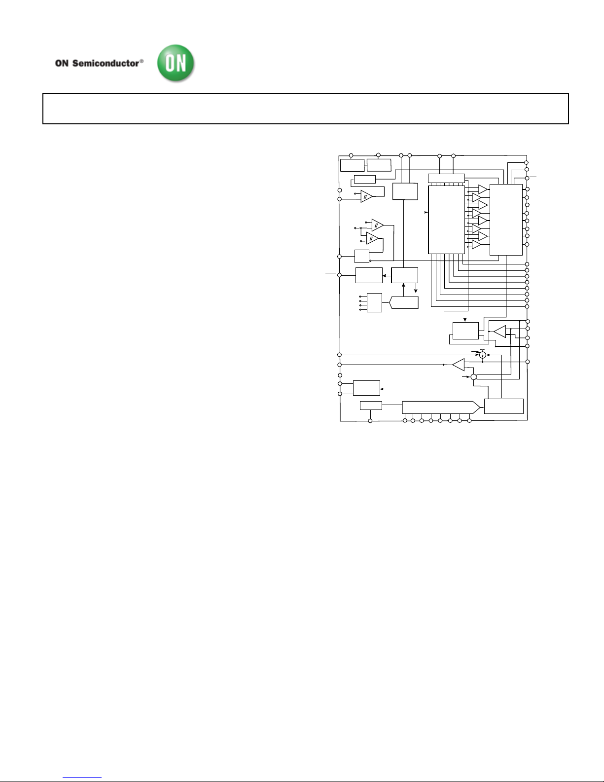
FUNCTIONAL BLOCK DIAGRAM
VCC
PRECISION
REFERENCE
DEL AY
–
+
GND
ASP0800
EN/VTT
13
PWRGD
6
RAMPADJ
18
RT
17
28
SW3
PWM2
37
CSREF
7
CSCOMP
PWM3
36
PWM4
35
CSSUM
22
FB
19
PWM1
VID2VID1 VID3 VID4 VID5 VID7VID6
2
COMP
FBRTN
VID DAC
CURRENT
MEASUREMENT
AND LIMIT
CROWBAR
CURRENT
LIMIT
+
–
40444546
47
OD1
SW2
29
SW4
27
12
16
+
–
OSCILLATOR
–
+
SW1
30
38
4143 42
11
IREF
VID0
10
IMON
CONTROL
CONTROL
CONTROL
CONTROL
CONTROL
ADC
PSI#
39
14
48
SMBUS
SCL
SD
A
5
4
BOOT VOLTAGE&
SOFT START CONTROL
ILIMITFS
20
1
VCC3
CONTROL
–
+
850mV
–
+
CONTROL
+
–
CSREF
UVLO
SHUTDOWN
SHUNT
REGULATOR
3.3V
REGULATOR
CLOCK
CONTROL
OC1
OC2
CONTROL
9
8
15
21
ODN
DIG ITAL
REGISTERS
24
SW7
SW6
25
SW8
23
SW5
26
+
–
CMP
PWM6
33
PWM7
32
PWM8
31
+
–
CMP
+
–
CMP
+
–
CMP
+
–
CMP
+
–
CMP
+
–
CMP
+
–
CMP
PWM5
34
CURRENT
BALANCING
CIRCUIT
1- 8 PHASE
DRIVER LOGIC
EN
SET
RESET
RESET
RESET
RESET
RESET
RESET
RESET
RESET
EN
FB
FBRTN
IMON
MUX
ALERT
3
COMPARATORS
Figure 1. Functional Block Diagram
GENERAL DESCRIPTION
The ASP08001 is an integrated power control IC with a PMBus
interface. The ASP0800 is a highly efficient, multiphase,
synchronous buck switching regulator controller, which aids
design of High Efficiency and High Density solutions.
The PMBus interface enables digital programming of key
system parameters to optimize system performance and provide
feedback to the system. The ASP0800 is compatible for use with
coupled inductors,
The ASP0800 is optimized for converting a 12 V main supply
into the core supply voltage required by high performance Intel
processors. It uses an internal 8-bit DAC to read the voltage
identification (VID) code directly from the processor, which is
used to set the output voltage between 0.375 V and 1.6 V.
This device uses a multimode PWM architecture to drive the
logic-level outputs at a programmable switching frequency that
can be optimized for VR size and efficiency. The ASP0800 can
be programmed for 1-, 2-, 3-, 4-, 5-, 6, 7 or 8- phase operation,
allowing for the construction of up to 8 complementary buck
switching stages. The ASP0800 support PSI#, which is a power
phases at light loads.
The ASP0800 includes a PMBus interface, which can be used to
program system set points such as voltage offset, load line,
phase balance and output voltage. Key system performance data
such as CPU current, CPU voltage, and power and fault
conditions can also be read back over the PMBus from the
ASP0800.
The ASP0800 OC Feature allows programming different offset
voltages depending on the load current being supplied. 3 OC
Thresholds and 4 OC Offsets value registers are supported.
The ASP0800 has a built in shunt regulator that allows the part
to be powered from the +12V system supply through a series
resistor. The ASP0800 is specified over the extended
commercial temperature range of 0°C to +85°C and is available
in a 48 Lead LFCSP package.
1
Protected by U.S. Patent Number 6,683,441; other patents pending.
Downloaded from DatasheetLib.com - datasheet search engine Downloaded from DatasheetLib.com - datasheet search engine
©2008 SCILLC. All rights reserved. Publication Order Number:
March 2008 - Rev. P1 ASP0800/S
Page 2

ASP0800 Preliminary Technical Data
TABLE OF CONTENTS
Features.............................................................................................. 1
Applications....................................................................................... 1
Functional Block Diagram .............................................................. 1
General Description ......................................................................... 1
Specifications..................................................................................... 3
Test Circuits....................................................................................... 6
Absolute Maximum Ratings............................................................ 7
Thermal Resistance ...................................................................... 7
ESD Caution.................................................................................. 7
Pin Configuration and Function Descriptions............................. 8
Typical Performance Characteristics ........................................... 10
Theory of Operation ...................................................................... 11
Start-Up Sequence...................................................................... 11
Phase Detection Sequence......................................................... 11
Master Clock Frequency............................................................ 12
Output Voltage Differential Sensing ........................................ 12
Output Current Sensing ............................................................ 12
Output current monitor ............................................................ 12
Dynamic VID ............................................................................. 13
INTERNAL Delay Timer .......................................................... 14
Soft Start ...................................................................................... 14
Current-Limit, Short-Circuit, and Latch-Off Protection...... 16
Power-Good Monitoring........................................................... 17
POWER STATE INDICATOR ................................................. 17
Output Crowbar......................................................................... 18
Output Enable and UVLO........................................................ 18
OVERCLOCKING (OC) LIMITS AND OFFSETS .............. 18
PMBUS Interface........................................................................ 18
Write Operations........................................................................ 21
Read Operations......................................................................... 22
PMBus Timeout.......................................................................... 23
Outline Dimensions....................................................................... 38
03/08—Rev P1: Conversion to ON Semiconductor
REVISION HISTORY
Downloaded from DatasheetLib.com - datasheet search engine Downloaded from DatasheetLib.com - datasheet search engine
Rev. P1 | Page 2 of 36 | www.onsemi.com
Page 3

Preliminary Technical Data ASP0800
SPECIFICATIONS
VCC = 5 V, FBRTN = GND, TA = 0°C to 85°C, unless otherwise noted.1
Table 1
Parameter Symbol Conditions Min Typ Max Unit
REFERENCE CURRENT
Reference Bias Voltage V
IREF
1.75 1.8 1.85 V
Reference Bias Current I
IREF
R
IREF
= 121 kΩ 15 uA
ERROR AMPLIFIER
Output Voltage Range2 V
COMP
0 4.4 V
Accuracy VFB
Relative to nominal DAC output,
referenced to FBRTN (see Figure 3)
−10 +10 mV
V
FB(BOOT)
In startup 1.09 1.1 1.11 V
Load Line Positioning Accuracy −77 −80 −83 mV
Load Line Range −350 0 mV
Load Line Attenuation 0 100 %
Differential Nonlinearity −1 +1 LSB
Input Bias Current IFB I
FB = IIREF
13.5 15 16.5 µA
Offset Accuracy VR Offset Register = TBD, VID = 1.0V −200 mV
VR Offset Register = TBD , VID = 1.0V 200 mV
FBRTN Current I
FBRTN
70 200 µA
Output Current I
COMP
FB forced to V
OUT
– 3% 500 µA
Gain Bandwidth Product GBW
(ERR)
COMP = FB 20 MHz
Slew Rate COMP = FB 25 V/µs
BOOT Voltage Hold Time t
BOOT
Internal Timer 2 ms
VID INPUTS
Input Low Voltage V
IL(VID)
VID(X) 0.3 V
Input High Voltage V
IH(VID)
VID(X) 0.8 V
Input Current I
IN(VID)
−5 µA
VID Transition Delay Time2 VID code change to FB change 400 ns
No CPU Detection Turn-Off
Delay Time
2
VID code change to PWM going low 5 µs
OSCILLATOR
Frequency Range2 f
OSC
0.25 9 MHz
Frequency Variation f
PHASE
T
A
= 25°C, RT = 500 kΩ, 4-phase 170 195 225 kHz
T
A
= 25°C, RT = 250 kΩ, 4-phase 375 kHz
T
A
= 25°C, RT = 121 kΩ, 4-phase 750 kHz
Output Voltage VRT R
T
= 500 kΩ to GND 1.9 2.0 2.1 V
RAMPADJ Output Voltage V
RAMPADJ
RAMPADJ − FB, VFB = 1V, −50 +50 mV
RAMPADJ Input Current Range I
RAMPADJ
5 125 µA
CURRENT SENSE AMPLIFIER
Offset Voltage V
OS(CSA)
CSSUM − CSREF (see Figure 3) −1.0 +1.0 mV
Input Bias Current, CSREF I
BIAS(CSREF)
CSREF = 1V −20 +20 µA
Input Bias Current, CSSUM I
BIAS(CSSUM)
CSREF = 1V −10 +10 nA
Gain Bandwidth Product GBW
(CSA)
CSSUM = CSCOMP 10 MHz
Slew Rate C
CSCOMP
= 10 pF 10 V/µs
Input Common-Mode Range CSSUM and CSREF 0 3.0 V
Output Voltage Range 0.05 3.0 V
Output Current I
CSCOMP
500 µA
Current Limit Latch off Delay Time Internal Timer 8 ms
1
All limits at temperature extremes are guaranteed via correlation using standard statistical quality control (SQC).
2
Guaranteed by design or bench characterization, not tested in production.
Downloaded from DatasheetLib.com - datasheet search engine Downloaded from DatasheetLib.com - datasheet search engine
Rev. P1 | Page 3 of 36 | www.onsemi.com
Page 4

ASP0800 Preliminary Technical Data
Parameter Symbol Conditions Min Typ Max Unit
PSI#
Input Low Voltage 0.3 V
Input High Voltage 0.8 V
Input Current −5 µA
Assertion Timing Fsw = 300kHz 3.3 µs
Deassertion Timing Fsw = 300kHz 825 ns
IMON OUTPUT
Clamp Voltage 1.0 1.15 V
Accuracy
10 × (CSREF − CSCOMP)/RILIM
−3 3 %
Output Current
800 µA
Offset
−3 3 mV
CURRENT LIMIT COMPARITOR
ILIM Bias Current I
LIM
CSREF − CSCOMP)/RILIM , (CSREF −
CSCOMP)=150 mV, RI
LIMC=7.5 kΩ
20 µA
Current Limit Threshold Current ICL
4/3 × IIREF
20 µA
CURRENT BALANCE AMPLIFIER
Common-Mode Range V
SW(X)CM
−600 +200 mV
Input Resistance R
SW(X)
SW(X) = 0 V 14 19 25 kΩ
Input Current I
SW(X)
SW(X) = 0 V 7 12 20 µA
Input Current Matching
'I
SW(X)
SW(X) = 0 V −6 +6 %
Phase Balance Adjustment Range Low Phase Bal Registers = 00000 -25 %
Phase Balance Adjustment Range
High
Phase Bal Registers = 11111 +25 %
DELAY TIMER
Internal Timer Delay Time Register = 011 2 ms
Timer Range Low Delay Time Register = 000 0.5 ms
Timer Range High Delay Time Register = 111 4 ms
SOFT START
Internal Timer Soft Start Slope Register = 010 0.5 V/ms
Timer Range Low Soft Start Slope Register = 000 0.1 V/ms
Timer Range High Soft Start Slope Register = 111 1.5 V/ms
ENABLE INPUT
Input Low Voltage V
IL(EN)
0.3 V
Input High Voltage V
IH(EN)
0.8 V
Input Current I
IN(EN)
−1 µA
Delay Time t
DELAY(EN)
EN > 0.8V , Internal Delay 2 ms
ODN / OD1 OUTPUTS
Output Low Voltage V
OL(
ODN/1
, )
I
OD(SINK)
= −400 PA
160 500 mV
Output High Voltage V
OH(
ODN/1
)
I
OD(SOURCE)
= 400 PA
4 5 V
ODN / OD1 Pull-Down Resistor
60 kΩ
OVER-CLOCKING OUTPUTS (OC1, OC2)
Output Low Voltage VOL I
OC(SINK)
= -1 mA 160 500 mV
POWER GOOD COMPARATOR
Undervoltage Threshold V
PWRGD(UV)
Relative to nominal DAC output −600 −500 −400 mV
Undervoltage Adjustment Range Low PWRGD_LO Register = 000 −500 mV
Undervoltage Adjustment Range
High
PWRGD_LO Register = 111 −150 mV
Overvoltage Threshold V
PWRGD(OV)
Relative to DAC output, PWRGD_Hi = 00 200 300 400 mV
Overvoltage Adjustment Range Low PWRGD_Hi Register = 11 150 mV
Overvoltage Adjustment Range High PWRGD_Hi Register = 00 300 mV
Output Low Voltage V
OL(PWRGD)
I
PWRGD(SINK)
= −4 mA 150 300 mV
Power Good Delay Time
Downloaded from DatasheetLib.com - datasheet search engine Downloaded from DatasheetLib.com - datasheet search engine
Rev. P1 | Page 4 of 36 | www.onsemi.com
Page 5

Preliminary Technical Data ASP0800
Rev. Pr H| Page 5 of 38
Parameter Symbol Conditions Min Typ Max Unit
During Soft Start2 Internal Timer 2 ms
VID Code Changing 100 250 µs
VID Code Static 200 ns
Crowbar Trip Point V
CROWBAR
Relative to DAC output, PWRGD_Hi = 00 200 300 400 mV
Overvoltage Adjustment Range Low PWRGD_Hi Register = 11 150 mV
Overvoltage Adjustment Range High PWRGD_Hi Register = 00 300 mV
Crowbar Reset Point Relative to FBRTN 250 300 350 mV
Crowbar Delay Time t
CROWBAR
Overvoltage to PWM going low
VID Code Changing 100 250 µs
VID Code Static 400 ns
PWM OUTPUTS
Output Low Voltage V
OL(PWM)
I
PWM(SINK)
= −400 µA 160 500 mV
Output High Voltage V
OH(PWM)
I
PWM(SOURCE)
= 400 µA 4 5 V
PMBus Interface
Logic High Input Voltage V
IH(SDA, SCL)
2.1 V
Logic Input Low Voltage V
IL(SDA, SCL)
0.8 V
Hysteresis 500 mV
SDA Output Low Voltage VOL I
SDA
= −6mA 0.4 V
Input Current I
IH
; IIL −1 1 µA
Input Capacitance C
SCL, SDA
5 pF
Clock Frequency f
SCL
400 kHz
SCL Falling Edge to SDA Valid Time 1 µs
ALERT
FAU LT
OUTPUTS
Output Low Voltage VOL I
OUT
= -6mA 0.4 V
Output High Leakage Current IOH V
OH
= 5V 1 uA
ANALOG/DIGITAL CONVERTER
Total Unadjusted Error (TUE) ±2 %
Differential Non linearity (DNL) TBD Bits 1 LSB
Conversion Time Averaging Enabled (32 averages) 80 ms
SUPPLY V
SYSTEM
= 12 V, R
SHUNT
= 340 Ω
VCC2 VCC 4.70 5 5.45 V
DC Supply Current I
VCC
V
SYSTEM
= 13.2 V, R
SHUNT
= 340 Ω 21 26 mA
UVLO Turn-On Current 6.5 11 mA
UVLO Threshold Voltage V
UVLO
VCC rising 9 V
UVLO Turn-Off Voltage VCC falling 4.1 V
VCC3 Output Voltage VCC3 I
VCC3
= 1mA 3.0 3.3 3.6 V
Downloaded from DatasheetLib.com - datasheet search engine Downloaded from DatasheetLib.com - datasheet search engine
Rev. P1 | Page 5 of 36 | www.onsemi.com
Page 6
ASP0800 Preliminary Technical Data
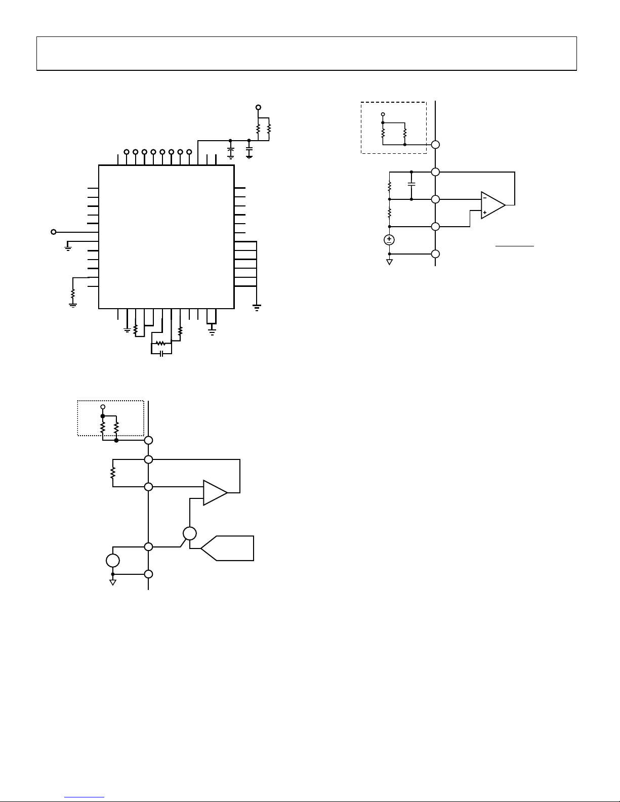
TEST CIRCUITS
VCC3
PWRGD
ALERT
SDA
SCL
EN
GND
OC1
OC2
IMON
IREF
RT
RAMPADJ
FBRTN
COMPFBCSREF
CSSUM
CSCOMP
ILIMITFS
ODN
OD1
SW8
SW7
PWM3
PWM4
PWM5
PWM6
PWM7
PWM8
SW1
SW2
SW3
SW4
SW5
SW6
PSI
VID0
VID1
VID2
VID3
VID4
VID5
VID6
VID7
VCC
PWM1
PWM2
ASP0800
8 BIT
VID CODE
100nF
+12V
680
:
680
:
1
µF
+
121k:
10k:
20k:
100nF
1k:
+1.25V
Figure 2. Closed-Loop Output Voltage Accuracy
+
–
39
VCC
CSREF
GND
7
FB
15
COMP
16
10k
A
SP0800
+
–
+
'VFB = FB'V=80mV - F B'V=0mV
VID
DAC
1.0V
+
–
+12V
680:
680:
17
Figure 3 . Current Sense Amplifier V
OS
CSSUM
19
CSCOMP
18
39
VCC
CSREF
17
GND
7
39k
680 680
100nF
1k
1V
ASP0800
VOS =
CSCOMP – 1V
40
12V
Figure 4 . Positioning Voltage
Downloaded from DatasheetLib.com - datasheet search engine Downloaded from DatasheetLib.com - datasheet search engine
Rev. P1 | Page 6 of 36 | www.onsemi.com
Page 7
Preliminary Technical Data ASP0800
Rev. Pr H| Page 7 of 38
ABSOLUTE MAXIMUM RATINGS
Table 2.
Parameter Rating
VCC −0.3 V to +6 V
FBRTN −0.3 V to +0.3 V
PWM2 to PWM8, RAMPADJ −0.3 V to VCC + 0.3 V
SW1 to SW8 −5 V to +25 V
<200 ns −10 V to +25 V
All Other Inputs and Outputs −0.3 V to VCC + 0.3 V
Storage Temperature Range −65°C to +150°C
Operating Ambient Temperature Range 0°C to 85°C
Operating Junction Temperature 125°C
Lead Temperature
Soldering (10 sec)
300°C
Infrared (15 sec) 260°C
Stresses above those listed under Absolute Maximum Ratings
may cause permanent damage to the device. This is a stress
rating only; functional operation of the device at these or any
other conditions above those indicated in the operational
section of this specification is not implied. Exposure to absolute
maximum rating conditions for extended periods may affect
device reliability.
THERMAL RESISTANCE
θJA is specified for the worst-case conditions, that is, a device
soldered in a circuit board for surface-mount packages.
Table 3. Thermal Resistance
Package Type θJA θ
JC
Unit
Thermal Impedance (θJA) 27°C/W
ESD CAUTION
Downloaded from DatasheetLib.com - datasheet search engine Downloaded from DatasheetLib.com - datasheet search engine
Rev. P1 | Page 7 of 36 | www.onsemi.com
Page 8
ASP0800 Preliminary Technical Data
PIN CONFIGURATION AND FUNCTION DESCRIPTIONS
13141516171819
2021222324
FBRTN
COMP
FB
CSREF
CSSUM
CSCOMP
ILIMFS
ODN
OD1
SW8
SW7
RAMPADJ
4847464544434241403938
37
PSI
VID0
VID1
VID2
VID3
VID4
VID5
VID6
PWM1
PWM2
1
2
3
4
5
6
7
8
9
10
11
12
VCC3
PWRGD
ALERT
SDA
SCL
EN
GND
OC1
OC2
IMON
IREF
RT
PWM4
PWM5
PWM6
PWM7
PWM8
SW1
SW2
SW3
SW4
SW5
SW6
35
PWM336
34
33
32
31
30
29
28
27
26
25
ASP0800
JCPZ
XXXXX
XXXXXXX
(Not to Scale)
PIN 1
INDICATOR
VCC
VID7
Figure 5. Pin Configuration
Table 4. Pin Function Descriptions
Pin No. Mnemonic Description
1 VCC3 3.3V Power Supply Output. A capacitor from this pin to ground provided decoupling for the interval 3.3V LDO.
2 PWRGD
Power-Good Output: Open-drain output that signals when the output voltage is outside of the proper operating
range.
3
ALERT
ALERT
Output : Open drain output that asserts low when the VR exceeds a programmable limit. Can be
configured for Comparator Mode or Interrupt Mode.
4 SDA
Digital Input / Output. PMBus serial data bidirectional pin. Requires PMBus pull up.
5 SCL
Digital Input. PMBus serial bus clock open drain input. Requires PMBus pull up.
6 EN Power Supply Enable Input. Pulling this pin to GND disables the PWM outputs and pulls the PWRGD output low.
7 GND Ground. All internal biasing and the logic output signals of the device are referenced to this ground
8 OC1 Over Clocking Bit 1 Output. The pin is connected to the clock control chip to set the over-clocking state.
9 OC2 Over Clocking Bit 2 Output. The pin is connected to the clock control chip to set the over-clocking state.
10 IMON
Total Current Output Pin.
11
IREF Current Reference Input. An external resistor from this pin to ground sets the reference current for I
FB
, and I
ILIMFS
.
12 RT
Frequency Setting Resistor Input. An external resistor connected between this pin and GND sets the oscillator
frequency of the device.
13 RAMPADJ PWM Ramp Current Input. An external resistor from the converter input voltage to this pin sets the internal PWM ramp.
14 FBRTN Feedback Return. VID DAC and error amplifier reference for remote sensing of the output voltage.
15 COMP Error Amplifier Output and Compensation Point.
16 FB
Feedback Input. Error amplifier input for remote sensing of the output voltage. An external resistor between this
pin and the output voltage sets the no load offset point.
17 CSREF
Current Sense Reference Voltage Input. The voltage on this pin is used as the reference for the current sense
amplifier and the power-good and crowbar functions. This pin should be connected to the common point of the
output inductors.
18 CSSUM
Current Sense Summing Node. External resistors from each switch node to this pin sum the average inductor
currents together to measure the total output current.
19 CSCOMP
Current Sense Compensation Point. A resistor and capacitor from this pin to CSSUM determines the gain of the
current sense amplifier and the positioning loop response time.
20 ILIMFS
Current Sense and Limit Scaling Pin. An external resistor from this pin to CSCOMP sets the internal current
sensing signal for current-limit and IMON. This value can be over-written using the PMBus interface.
21
ODN
Output Disable Logic Output for PSI# operation. This pin is actively pulled low when PSI# is low, otherwise it
functions in the same way as
OD1
.
22
OD1
Output Disable Logic Output. This pin is actively pulled low when the EN input is low or when VCC is below its
UVLO threshold to signal to the Driver IC that the driver high-side and low-side outputs should go low.
Downloaded from DatasheetLib.com - datasheet search engine Downloaded from DatasheetLib.com - datasheet search engine
Rev. P1 | Page 8 of 36 | www.onsemi.com
Page 9

Preliminary Technical Data ASP0800
Rev. Pr H| Page 9 of 38
Pin No. Mnemonic Description
23 to
30
SW8 to SW1 Current Balance Inputs. Inputs for measuring the current level in each phase. The SW pins of unused phases
should be left open.
31 to
38
PWM8 to
PWM1
Logic-Level PWM Outputs. Each output is connected to the input of an external MOSFET driver such as the
ADP3121. Connecting the PWM8, PWM7, PWM6, PWM5, PWM4, PWM3 and PWM2 outputs to VCC causes that
phase to turn off, allowing the ASP0800 to operate as a 1, 2-, 3-, 4-, 5-, 6, 7 or 8-phase controller.
39 VCC
Supply Voltage for the Device. A 340 Ω resistor should be placed between the 12 V system supply and the VCC
pin. The internal shunt regulator maintains VCC = 5 V.
40 to
47
VID7 to VID0
Voltage Identification DAC Inputs. These eight pins are pulled down to GND, providing a logic zero if left open. When
in normal operation mode, the DAC output programs the FB regulation voltage from 0.375 V to 1.6
48
PSI
Power State Indicator. Pulling this pin low places the controller in lower power state operation.
Downloaded from DatasheetLib.com - datasheet search engine Downloaded from DatasheetLib.com - datasheet search engine
Rev. P1 | Page 9 of 36 | www.onsemi.com
Page 10

ASP0800 Preliminary Technical Data
TYPICAL PERFORMANCE CHARACTERISTICS
TBD
Rev. P1 | Page 10 of 36 | www.onsemi.com
Downloaded from DatasheetLib.com - datasheet search engine Downloaded from DatasheetLib.com - datasheet search engine
Page 11
Preliminary Technical Data ASP0800
Rev. Pr H| Page 11 of 38
THEORY OF OPERATION
The ASP0800 combines a multi-mode, fixed frequency PWM
control with multi-phase logic outputs for use in multi-phase
synchronous buck CPU core supply power converters. The
internal VID DAC is designed to interface with the Intel 8-bit
VR 11 and VR 11.1 compatible CPUs .
In addition, the ASP0800 incorporates a serial interface to allow
the programming of key system performance specifications and
read back CPU data such as voltage, current and power.
Multiphase operation is important for producing the high
currents and low voltages demanded by today’s
microprocessors. Handling the high currents in a single-phase
converter would place high thermal demands on the
components in the system such as the inductors and MOSFETs.
The multimode control of the ASP0800 ensures a stable, high
performance topology for:
x Balancing currents and thermals between phases for
both static and dynamic operation.
x High speed response at the lowest possible switching
frequency and output decoupling
x FEPWM improves load step response.
x Minimizing thermal switching losses by utilizing
lower frequency operation
x High current output due to 8 phase operation
x Tight load line regulation and accuracy
x Reduced output ripple due to multiphase cancellation
x PC board layout noise immunity
x Ease of use and design due to independent component
selection
x Flexibility in operation for tailoring design to low cost
or high performance
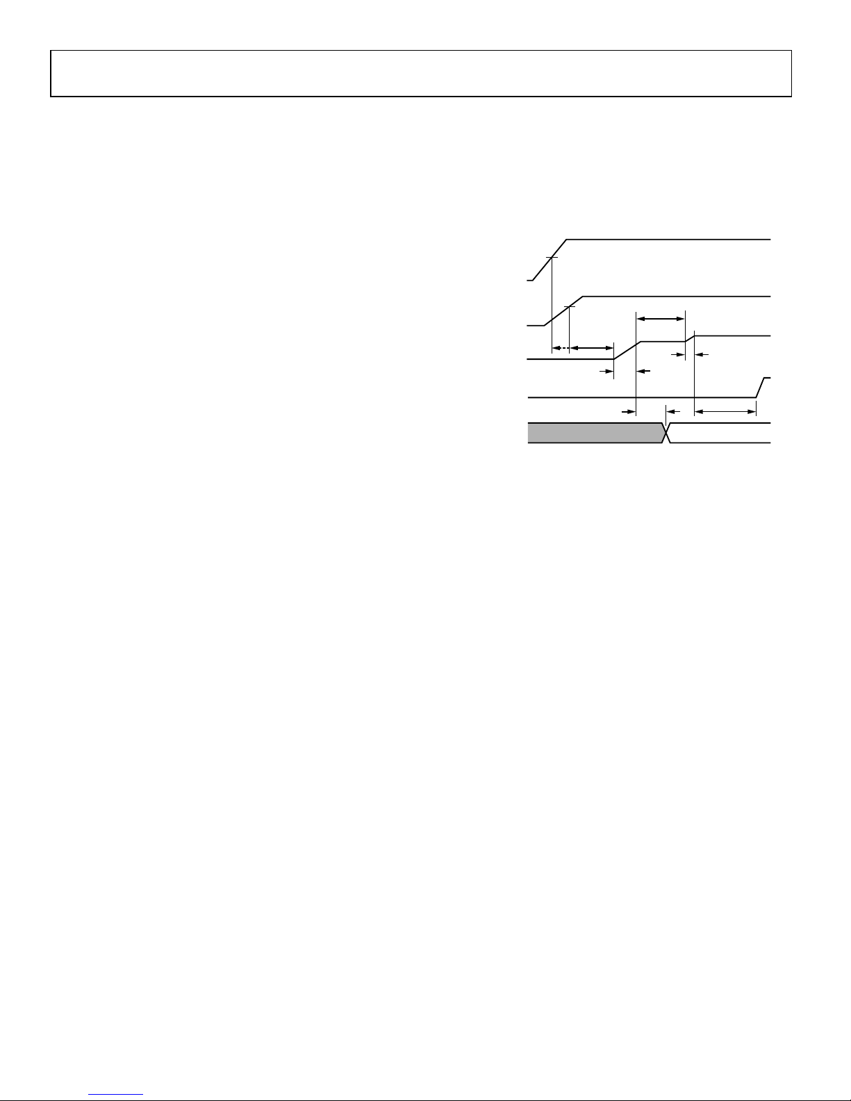
START-UP SEQUENCE
The ASP0800 follows the VR11 start-up sequence shown in
Figure 7. After both the EN and UVLO conditions are met, a
programmable internal timer goes through one cycle TD1. This
delay cycle is programmed using Delay Command, default
delay = 2ms). The first eight clock cycles of TD2 are blanked
from the PWM outputs and used for phase detection as
explained in the following section. Then the programmable
internal soft-start ramp is enabled (TD2) and the output comes
up to the boot voltage of 1.1V. The boot hold time is also set by
the Delay Command. This second delay cycle is called TD3.
During TD3 the processor VID pins settle to the required VID
code. When TD3 is over, the ASP0800 reads the VID inputs
and soft starts either up or down to the final VID voltage
(TD4). After TD4 has been completed and the PWRGD
masking time (equal to VID on the fly masking) is finished, a
third cycle of the internal timer sets the PWRGD blanking
(TD5).
The internal delay and soft start times are programmable using
the serial interface and the Delay Command and Soft Start
Command.
TD1
TD3
TD2
TD5
50µs
TD4
5V
SUPPLY
VTT I/O
(ADP3298 EN)
VCC_CORE
VR READY
(ADP3298 PWRG D)
CPU
VID I NPUTS
VID INVALID VID VALID
V
BOOT
(1.1V)
UVLO
THRESHOL D
0.85V
V
VID
Figure 7. System Start-Up Sequence for VR11
PHASE DETECTION SEQUENCE
During startup, the number of operational phases and their
phase relationship is determined by the internal circuitry that
monitors the PWM outputs. Normally, the ASP0800 operates as
a 8-phase PWM controller.
To operate as a 7-phase controller connect PWM8 to VCC.
To operate as a 6-phase controller connect PWM7 and PWM8
to VCC.
To operate as a 5-phase controller connect PWM6, PWM7 and
PWM8 to VCC.
To operate as a 4-phaase controller connect PWM5, PWM6,
PWM7 and PWM8 to VCC.
To operate as a 3-phase controller connect PWM4, PWM5,
PWM6, PWM7 and PWM8 to VCC.
To operate as a 2-phase controller connect PWM3, PWM4,
PWM5, PWM6, PWM7 and PWM8 to VCC.
To operate as a 1-phase controller connect PWM2, PWM3,
PWM4, PWM5, PWM6, PWM7 and PWM8 to VCC.
Prior to soft start, while EN is low, the PWM8, PWM7, PWM6,
PWM5, PWM4, PWM3 and PWM2 pins sink approximately
100 µA each. An internal comparator checks each pin’s voltage
vs. a threshold of 3 V. If the pin is tied to VCC, it is above the
threshold. Otherwise, an internal current sink pulls the pin to
GND, which is below the threshold. PWM1 is low during the
phase detection interval that occurs during the first eight clock
cycles of TD2. After this time, if the remaining PWM outputs
are not pulled to VCC, the 100 µA current sink is removed, and
they function as normal PWM outputs. If they are pulled to
Downloaded from DatasheetLib.com - datasheet search engine Downloaded from DatasheetLib.com - datasheet search engine
Rev. P1 | Page 11 of 36 | www.onsemi.com
Page 12

ASP0800 Preliminary Technical Data
VCC, the 100 µA current source is removed, and the outputs
are put into a high impedance state.
The PWM outputs are logic-level devices intended for driving
fast response external gate drivers such as the ADP3121 and
ADP3122. Because each phase is monitored independently,
operation approaching 100% duty cycle is possible. In addition,
more than one output can be on at the same time to allow
overlapping phases.
MASTER CLOCK FREQUENCY
The clock frequency of the ASP0800 is set with an external
resistor connected from the RT pin to ground. The frequency
follows the graph in Figure 6. To determine the frequency per
phase, the clock is divided by the number of phases in use. If all
phases are in use, divide by 6. If 4 phases are in use divide by 4.
OUTPUT VOLTAGE DIFFERENTIAL SENSING
The ASP0800 combines differential sensing with a high
accuracy VID DAC and reference, and a low offset error amplifier. This maintains a worst-case specification of ±10 mV
differential sensing error over its full operating output voltage
and temperature range. The output voltage is sensed between
the FB pin and FBRTN pin. FB is connected through a resistor,
R
B,
to the regulation point, usually the remote sense pin of the
microprocessor. FBRTN is connected directly to the remote
sense ground point. The internal VID DAC and precision
reference are referenced to FBRTN, which has a minimal
current of 70 µA to allow accurate remote sensing. The internal
error amplifier compares the output of the DAC to the FB pin to
regulate the output voltage.
OUTPUT CURRENT SENSING
The ASP0800 provides a dedicated current-sense amplifier
(CSA) to monitor the total output current for proper voltage
positioning vs. load current, for the IMON output and for
current-limit detection. Sensing the load current at the output
gives the total real time current being delivered to the load,
which is an inherently more accurate method than peak current
detection or sampling the current across a sense element such
as the low-side MOSFET. This amplifier can be configured
several ways, depending on the objectives of the system, as
follows:
x Output inductor DCR sensing without a thermistor for
lowest cost.
x Output inductor DCR sensing with a thermistor for
improved accuracy with tracking of inductor temperature.
x Sense resistors for highest accuracy measurements.
The positive input of the CSA is connected to the
CSREF pin, which is connected to the average output
voltage. The inputs to the amplifier are summed together
through resistors from the sensing element, such as the
switch node side of the output inductors, to the inverting
input CSSUM. The feedback resistor between CSCOMP and
CSSUM sets the gain of the amplifier and a filter capacitor is
placed in parallel with this resistor. The gain of the amplifier
is programmable by adjusting the feedback resistor.
This difference signal is used internally to offset the
VID DAC for voltage positioning. This different signal can
be adjusted between 50%-150% of the external value using
the PMBus Loadline Calibration (0xDE) and Loadline Set
(0xDF) commands.
The difference between CSREF and CSCOMP is then used
as a differential input for the current-limit comparator.
To provide the best accuracy for sensing current, the CSA is
designed to have a low offset input voltage. Also, the sensing
gain is determined by external resistors to make it extremely
accurate.
The CPU current can also be monitored over the PMBus.
The current limit and the load line can be programmed over
PMBus.
OUTPUT CURRENT MONITOR
IMON is an analog output from the ASP0800 representing the
total current being delivered to the load. It outputs an accurate
current that is directly proportional to the current set by the
ILIMFS resistor. The current is then run through a parallel RC
connected from the IMON pin to the FBRTN pin to generate an
accurately scaled and filtered voltage as per the VR11.1
specification. The size of the resistor is used to set the IMON
scaling.
If the IMON and the OCP need to be changed based on the
TDC of the CPU, then the ILIMFS resistor is the only
component that needs to be changed. If the IMON scaling is the
only change needed then changing the IMON resistor
accomplishes this.
The IMON pin also includes an active clamp to limit the IMON
voltage to 1.15V MAX while maintaining 900mV MIN full scale
accurate reporting.
ACTIVE IMPEDANCE CONTROL MODE
For controlling the dynamic output voltage droop as a
function of output current, the CSA gain and load line
programming can be scaled to be equal to the droop
impedance of the regulator times the output current. This
droop voltage is then used to set the input control voltage to
the system. The droop voltage is subtracted from the DAC
reference input voltage directly to tell the error amplifier
where the output voltage should be. This allows enhanced
feed-forward response.
Downloaded from DatasheetLib.com - datasheet search engine Downloaded from DatasheetLib.com - datasheet search engine
Rev. P1 | Page 12 of 36 | www.onsemi.com
Page 13

Preliminary Technical Data ASP0800
Rev. Pr H| Page 13 of 38
CURRENT CONTROL MODE AND THERMAL
BALANCE
The ASP0800 has individual inputs (SW1 to SW8) for each
phase that are used for monitoring the current of each
phase. This information is combined with an internal ramp
to create a current balancing feedback system that has been
optimized for initial current balance accuracy and dynamic
thermal balancing during operation. This current balance
information is independent of the average output current
information used for positioning as described in the Output
Current Sensing section.
The magnitude of the internal ramp can be set to optimize
the transient response of the system. It also monitors the
supply voltage for feed-forward control for changes in the
supply. A resistor connected from the power input voltage
to the RAMPADJ pin determines the slope of the internal
PWM ramp.
The balance between the phases can be programmed using
the PMBus Phase Bal SW(x) commands (TBD to TBD).
This allows each phase to be adjusted if there is a difference
in temperature due to layout and airflow considerations.
The phase balance can be adjusted from a default gain of 5
(Bits 4:0 = 10000). The minimum gain programmable is 3.75
(Bits 4:0 = 00000) and the max gain is 6.25 (Bits 4:0 =
11111).
VOLTAGE CONTROL MODE
A high gain, high bandwidth, voltage mode error amplifier
is used for the voltage mode control loop. The control input
voltage to the positive input is set via the VID logic
according to the voltages listed in
Ta bl e 5. The VID code is
set using the VID Input pins or it can be programmed over
the PMBus using the VOUT_Command. By default, the
ASP0800 outputs a voltage corresponding to the VID
Inputs. To output a voltage following the VOUT_Command
the user first needs to program the required VID Code.
Then the VID_EN Bits need to be enabled. The following is
the sequence
1. Program the required VID Code to the
VOUT_Command code (0x21)
2. Set the VID_EN bit (Bit 3) in the VR Config 1A (0xD2)
and on the VR Config 1B (0xD3).
This voltage is also offset by the droop voltage for active
positioning of the output voltage as a function of current,
commonly known as active voltage positioning. The output
of the amplifier is the COMP pin, which sets the
termination voltage for the internal PWM ramps.
The negative input (FB) is tied to the output sense location
with Resistor R
B
and is used for sensing and controlling the
output voltage at this point. A current source (equal to
IREF) from the FB pin flowing through R
B
is used for setting
the no load offset voltage from the VID voltage. The no load
voltage is negative with respect to the VID DAC for Intel
CPU’s. The main loop compensation is incorporated into
the feedback network between FB and COMP.
An offset voltage can be added to the control voltage over
the serial interface. This is done using Bits <5:0> of the
VOUT_TRIM (0xDB) and VOUT_CAL (0xDC)
Commands. The max offset that can be applied is +/200mV (even if the sum of the offsets > 200mV). The LSB
size id 6.25mV. A positive offset is applied when Bit 4 = 0. A
negative offset is applied when Bit 4 = 1.
Table 5. Offset Codes
VOUT_TRI
M CODE
TRIM
OFFSET
V O LTA G
E
VOUT_CA
L CODE
CAL
OFFSET
V O LTA G
E
TOTAL
OFFSET
V O LTA G
E
TBD TBD TBD TBD TBD
TBD TBD TBD TBD TBD
TBD TBD TBD TBD TBD
DYNAMIC VID
The ASP0800 has the ability to dynamically change the VID
inputs while the controller is running. This allows the output
voltage to change while the supply is running and supplying
current to the load. This is commonly referred to as Dynamic
VID (DVID). A DVID can occur under either light or heavy
load conditions. The processor signals the controller by
changing the VID inputs (or by programming a new
VOUT_Command) in a single or multiple steps from the start
code to the finish code. This change can be positive or negative.
When a VID bit changes state, the ASP0800 detects the change
and ignores the DAC inputs for a minimum of 200 ns. This time
prevents a false code due to logic skew while the VID inputs are
changing. Additionally, the first VID change initiates the
PWRGD and CROWBAR blanking functions for a minimum of
100 µs to prevent a false PWRGD or CROWBAR event. Each
VID change resets the internal timer.
If a VID off code is detected the ASP0800 will wait for 5usec to
ensure that the code is correct before initiating a shutdown of
the controller.
Rev. P1 | Page 13 of 36 | www.onsemi.com
Downloaded from DatasheetLib.com - datasheet search engine Downloaded from DatasheetLib.com - datasheet search engine
Page 14

ASP0800 Preliminary Technical Data
The ASP0800 also uses the TON_Transition (0xD6) to limit the
DVID slew rates. These can be encountered when the system
does a large single VID step for power state changes, thus the
DVID slew rate needs to be limited to prevent large inrush
currents.
The transition slew rate is programmed using Bits <2:0> of
the Ton_Transition (0xD6) command code.
Ta bl e 6
provides the transition rate values.
Table 6. Transition Rate Codes
Code Transition Rate (V/msec)
000 1
001 3
010 5 = default
011 7
100 9
101 11
110 13
111 15
ENHANCED TRANSIENTS MODE
The ASP0800 incorporates enhanced transient response for
both load step up and load release. For load step up it senses
the output of the error amp to determine if a load step up
has occurred and then sequences on the appropriate
number of phases to ramp up the output current.
CURRENT REFERENCE
The IREF pin is used to set an internal current reference.
This reference current sets I
FB
. A resistor to ground
programs the current based on the 1.8 V output.
Typically, R
IREF
is set to 121 k to program IREF = 15 µA.
The following currents are then equal to
I
FB
= IREF = 15 µA
INTERNAL DELAY TIMER
The delay times for the start up timing sequence are set by an
internal timer. The default time is 2msec which can be changed
through the PMBus interface. This timer is used for multiple
delay timings (TD1, TD3, and TD5) during the start-up
sequence. Also, it is used for timing the current limit latch off
as explained in the CURRENT LIMIT section. The current
limit timer is set to 4 times the delay timer.
The delay timer is programmed using Bits <2:0> of the Ton
Delay command (0xD4). The delay can be programmed
between 0.5msec and 4msec.
Ta bl e 7 provides the
programmable delay values
Table 7. Delay Codes
Code Delay (msec)
000 0.5
001 1
010 1.5
011 2 = default
100 2.5
101 3
110 3.5
111 4
SOFT START
The Soft Start slope for the output voltage is set by an internal
timer. The default value is 0.5V/msec., which can be
programmed through the PMBus interface. After TD1 and the
phase detection cycle have been completed, the SS time (TD2 in
Figure 7) starts. The SS circuit uses the internal VID DAC to
increase the output voltage in 6.25mV steps up to the 1.1 V boot
voltage.
Once the SS circuit has reached the boot voltage, the boot
voltage delay time (TD3) is started. The end of the boot voltage
delay time signals the beginning of the second soft start time
(TD4). The SS voltage changes from the boot voltage to the
programmed VID DAC voltage (either higher or lower) using
6.25mV steps.
The soft start slew rate is programmed using Bits <2:0> of
the Ton_Rise (0xD5) command code.
Downloaded from DatasheetLib.com - datasheet search engine Downloaded from DatasheetLib.com - datasheet search engine
Rev. P1 | Page 14 of 36 | www.onsemi.com
Page 15

Preliminary Technical Data ASP0800
Table 8. Soft Start Codes provides the soft start values. Figure
8 shows typical start-up waveforms for the ASP0800.
Preliminary Technical Data ASP0800
ASP0800 Preliminary Technical Data
Table 8. Soft Start Codes
Code Soft Start (V/msec)
000 0.3
001 0.3
010 0.5 = default
011 0.7
100 0.9
101 1.1
110 1.3
111 1.5
Figure 8 shows typical start up waveforms for the ASP0800.
Figure 8. Typical Start up waveforms
Channel 1: CSREF
Channel 2: EN
Channel 3: PWM1
CURRENT-LIMIT, SHORT-CIRCUIT, AND LATCHOFF PROTECTION
The ASP0800 compares a programmable current limit set point
to the voltage from the output of the current sense amplifier.
The level of current limit is set with the resistor from the
ILIMFS pin to CSCOMP, and can be adjusted using the PMBus
interface.
The current limit threshold can be modified from the
resistor programmed value by using the PMBus interface
using Bits <4:0> of the Current Limit Threshold command
(0xE2). The limit is programmable between 50% of the
external limit and 146.7% of the external limit. The
resolution is 3.3%.
Ta bl e 9 gives some examples codes
Ta bl e 9 gives some examples codes
Preliminary Technical Data ASP0800
Table 9. Current Limit
Code Current Limit (% of external
limit)
0 0000 50%
0 0001 53.3%
1 0000 100% = default
1 0001 103.3%
1 1110 143.3%
1 1111 146.7%
The current limit threshold can be modified from the resistor
programmed value by using the serial interface.
If the limit is reached and TD5 has completed, an internal latchoff delay time will start, and the controller will shut down if the
fault is not removed. This delay is four times longer than the
delay time during the start-up sequence. The current limit
delay time only starts after the TD5 has completed. If there is a
current limit during start-up, the ASP0800 will go through TD1
to TD5, and then start the latch-off time. Because the controller
continues to cycle the phases during the latch-off delay time, if
the short is removed before the timer is complete, the controller
can return to normal operation.
The latch-off function can be reset by either removing and
reapplying the supply voltage to the ASP0800, or by toggling the
EN pin low for a short time.
The OCP latch-off function can be disabled by using the
PMBus interface. Setting the CLIM_EN bit (bit 1) of the VR
Config 1A (0xD2) and VR Config 1B (0xD3) registers to 0
disables the current limit latch off function. The ASP0800 can
continue to operate in current limit indefinitely.
During start-up when the output voltage is below 200 mV, a
secondary current limit is active. This is necessary because the
voltage swing of CSCOMP cannot go below ground. This
secondary current limit limits controls the internal COMP
voltage to the PWM comparators to 1.5 V. This limits the
voltage drop across the low-side MOSFETs through the current
balance circuitry. Typical over-current latch-off waveforms are
shown in Figure 9.
Figure 9. Overcurrent Latch-off Waveforms
Channel 1: CSREF,
Channel 2: COMP, Channel 3: PWM1
An inherent per phase current limit protects individual phases
if one or more phases stops functioning because of a faulty
component. This limit is based on the maximum normal mode
COMP voltage.
POWER-GOOD MONITORING
The power good comparator monitors the output voltage via
the CSREF pin. The PWRGD pin is an open-drain output
whose high level (when connected to a pull-up resistor)
indicates that the output voltage is within the nominal limits
specified in the specifications above based on the VID voltage
setting. PWRGD goes low if the output voltage is outside of this
specified range, if the VID DAC inputs are in no CPU mode, or
whenever the EN pin is pulled low. PWRGD is blanked during a
DVID event for a period of 100 µs to prevent false signals
during the time the output is changing.
The PWRGD circuitry also incorporates an initial turn-on
delay time (TD5). Prior to the SS voltage reaching the
programmed VID DAC voltage and the PWRGD masking time
finishing, the PWRGD pin is held low. Once the SS circuit
reaches the programmed DAC voltage, the internal timer
operates.
The value for the PWRGD high limit and low limit can be
programmed using the serial interface.
POWER STATE INDICATOR
Downloaded from DatasheetLib.com - datasheet search engine Downloaded from DatasheetLib.com - datasheet search engine
Rev. P1 | Page 15 of 36 | www.onsemi.com
Page 16

Figure 9. Overcurrent Latch-off Waveforms
Channel 1: CSREF,
Channel 2: COMP, Channel 3: PWM1
An inherent per phase current limit protects individual phases
if one or more phases stops functioning because of a faulty
component. This limit is based on the maximum normal mode
COMP voltage.
POWER-GOOD MONITORING
The power good comparator monitors the output voltage via
the CSREF pin. The PWRGD pin is an open-drain output
whose high level (when connected to a pull-up resistor)
indicates that the output voltage is within the nominal limits
specified in the specifications above based on the VID voltage
setting. PWRGD goes low if the output voltage is outside of this
specified range, if the VID DAC inputs are in no CPU mode, or
whenever the EN pin is pulled low. PWRGD is blanked during a
DVID event for a period of 100 µs to prevent false signals
during the time the output is changing.
The PWRGD circuitry also incorporates an initial turn-on
delay time (TD5). Prior to the SS voltage reaching the
programmed VID DAC voltage and the PWRGD masking time
finishing, the PWRGD pin is held low. Once the SS circuit
reaches the programmed DAC voltage, the internal timer
operates.
The value for the PWRGD high limit and low limit can be
programmed using the serial interface.
POWER STATE INDICATOR
The PSI# pin is an input used to determine the operating state
of the load. If this input is pulled low, the load is in a low power
state and the controller asserts the
ODN
pin low, which can be
used to disable phases and maintain better efficiency at lighter
loads.
The sequencing into and out of low power operation is
maintained to minimize output deviations as well as providing
full power load transients immediately after exiting a low power
ASP0800 Preliminary Technical Data
ASP0800 Preliminary Technical Data
OUTPUT CROWBAR
As part of the protection for the load and output components of
the supply, the PWM outputs are driven low (turning on the
low-side MOSFETs) when the output voltage exceeds the upper
crowbar threshold. This crowbar action stops once the output
voltage falls below the release threshold of approximately
300 mV.
The value for the crowbar limit follows the programmable
PWRGD high limit.
Turning on the low-side MOSFETs pulls down the output as the
reverse current builds up in the inductors. If the output
overvoltage is due to a short in the high-side MOSFET, this
action current-limits the input supply or blows its fuse,
protecting the microprocessor from being destroyed.
OUTPUT ENABLE AND UVLO
For the ASP0800 to begin switching, the input supply current to
the controller must be higher than the UVLO threshold and the
EN pin must be higher than its 0.8 V threshold. This initiates a
system start-up sequence. If either UVLO or EN is less than
their respective thresholds, the ASP0800 is disabled. This holds
the PWM outputs at ground and forces PWRGD,
ODN
and
OD1
signals low.
In the application circuit (see Figure TBD), the
OD1
pin should
be connected to the
OD
inputs of the external drivers for the
phases that are always on. The
ODN
pin should be connected to
the
OD
inputs of the external drivers on the phases that are shut
down during low power operation. Grounding the driver
OD
inputs disables the drivers such that both DRVH and DRVL are
grounded. This feature is important in preventing the discharge
of the output capacitors when the controller is shut off. If the
driver outputs are not disabled, a negative voltage can be
generated during output due to the high current discharge of
the output capacitors through the inductors.
OVERCLOCKING (OC) LIMITS AND OFFSETS
The ASP0800 includes an overclocking function. The total
output current is monitored by the ASP0800 using the I
MON
output.
Read_IOUT Command gives the total current in Amps
The IOUT value is compared with the Over Clocking or OC
Thresholds. There are three OC thresholds
Command TBD = OC Threshold 1; Default = TBD
Command TBD = OC Threshold 2; Default = TBD
Command TBD = OC Threshold 3; Default = TBD
I
OUT
is first compared with OC3, If I
OUT
is greater than OC3
then the system is in OC State TBD and Offset TBD is applied.
If I
OUT
is less than OC3 but greater than OC2 then the system is
in OC State TBD
.
If I
OUT
is less than OC2 but greater than OC1
then the system is in OC State TBD. If I
OUT
is less than OC1
then the system is in OC State TBD. Each offset state has a
corresponding Offset voltage. The offset voltage for each state is
programmable in TBD mV steps up to a max value of ±200
mV.
Register TBD VR Offset 1 = Offset voltage for State 1, default
value = 0x00
Register TBD VR Offset 2 = Offset voltage for State 2, default
value = 0x00
Register TBD VR Offset 3 = Offset voltage for State 3, default
value = 0x00
Register TBD VR Offset 4 = Offset voltage for State 4, default
value = 0x00
PMBUS INTERFACE
Control of the ASP0800 is carried out using the PMBus
Interface. The physical protocol for PMBus closely matches that
of SMBus.
The ASP0800 is connected to this bus as a slave device, under
the control of a master controller.
To setup the PMBus Address the ASP0800 sources a 10uA
current from the ADD pin through an external resistor. The
voltage is then measured by the ADC and user to set the PMBus
address. The table below gives the thresholds for each possible
PMBus address and also a suitable resistor value.
Table 10: Setting up the PMBus Address
Address
(8 Bits)
High
Threshold
Low
Threshold
Suggested Resistor
Va lu e
0xC0
0.1
0xC2
0.25 0.15
0xC4
0.5 0.3
0xC6
0.75 0.55
0xC8
1.0 0.8
0xCA
1.4 1.1
0xCC
1.9 1.5
0xCE
2.0
Data is sent over the serial bus in sequences of nine clock pulses:
eight bits of data followed by an acknowledge bit from the slave
device. Transitions on the data line must occur during the low
period of the clock signal and remain stable during the high
period, because a low-to-high transition when the clock is high
might be interpreted as a stop signal. The number of data bytes
that can be transmitted over the serial bus in a single read or
Downloaded from DatasheetLib.com - datasheet search engine Downloaded from DatasheetLib.com - datasheet search engine
Rev. P1 | Page 16 of 36 | www.onsemi.com
Page 17

corresponding Offset voltage. The offset voltage for each state is
programmable in TBD mV steps up to a max value of ±200
mV.
Register TBD VR Offset 1 = Offset voltage for State 1, default
value = 0x00
Register TBD VR Offset 2 = Offset voltage for State 2, default
value = 0x00
Register TBD VR Offset 3 = Offset voltage for State 3, default
value = 0x00
Register TBD VR Offset 4 = Offset voltage for State 4, default
value = 0x00
PMBUS INTERFACE
Control of the ASP0800 is carried out using the PMBus
Interface. The physical protocol for PMBus closely matches that
of SMBus.
The ASP0800 is connected to this bus as a slave device, under
the control of a master controller.
To setup the PMBus Address the ASP0800 sources a 10uA
current from the ADD pin through an external resistor. The
voltage is then measured by the ADC and user to set the PMBus
address. The table below gives the thresholds for each possible
PMBus address and also a suitable resistor value.
Table 10: Setting up the PMBus Address
Address
(8 Bits)
High
Threshold
Low
Threshold
Suggested Resistor
Va lu e
0xC0
0.1
0xC2
0.25 0.15
0xC4
0.5 0.3
0xC6
0.75 0.55
0xC8
1.0 0.8
0xCA
1.4 1.1
0xCC
1.9 1.5
0xCE
2.0
Data is sent over the serial bus in sequences of nine clock pulses:
eight bits of data followed by an acknowledge bit from the slave
device. Transitions on the data line must occur during the low
period of the clock signal and remain stable during the high
period, because a low-to-high transition when the clock is high
might be interpreted as a stop signal. The number of data bytes
that can be transmitted over the serial bus in a single read or
Preliminary Technical Data ASP0800
Preliminary Technical Data ASP0800
write operation is limited only by what the master and slave
devices can handle.
1. When all data bytes have been read or written, stop
conditions are established. In write mode, the master pulls the
data line high during the tenth clock pulse to assert a stop
condition. In read mode, the master device overrides the
acknowledge bit by pulling the data line high during the low
period before the ninth clock pulse; this is known as No
Acknowledge. The master takes the data line low during the low
period before the tenth clock pulse, and then high during the
tenth clock pulse to assert a stop condition.
Any number of bytes of data can be transferred over the serial
bus in one operation, but it is not possible to mix read and write
in one operation because the type of operation is determined
at the beginning and cannot subsequently be changed without
starting a new operation.
In the ASP0800, write operations contain one, two or three
bytes, and read operations contain one or two bytes. The
command code or register address determines the number of
bytes to be read or written, See the register map for more
information.
To write data to one of the device data registers or read data
from it, the address pointer register must be set so that the
correct data register is addressed (i.e. command code), and then
data can be written to that register or read from it. The first byte
of a read or write operation always contains an address that is
stored in the address pointer register. If data is to be written to
the device, the write operation contains a second data byte that
is written to the register selected by the address pointer register.
This write byte operation is shown in Figure 11. The device
address is sent over the bus, and then R/
W
is set to 0. This is
followed by two data bytes. The first data byte is the address of
the internal data register to be written to, which is stored in the
address pointer register. The second data byte is the data to be
written to the internal data register.
2. The read byte operation is shown in Figure 12. First
the command code needs to be written to the ASP0800 so that
the required data is sent back. This is done by performing a
write to the ASP0800 as before, but only the data byte
containing the register address is sent, because no data is
written to the register. A repeated start is then issued and a read
operation is then performed consisting of the serial bus address;
R/
W
bit set to 1, followed by the data byte read from the data
register.
Downloaded from DatasheetLib.com - datasheet search engine Downloaded from DatasheetLib.com - datasheet search engine
Rev. P1 | Page 17 of 36 | www.onsemi.com
Page 18

ASP0800 Preliminary Technical Data
R/W
1
SCL
SDA
10
0
0
A1
A0
D7
D6
D5
D4
D3
D2
D1
D0
ACK. BY
ADP3298
STOP BY
MASTER
STA RT BY
MASTER
FRAME 1
SERIAL BUS ADDRESS
BYTE
FRAME 2
COMMAND CODE
1
1
ACK. BY
ADP3298
9
9
Figure 10. Send Byte
R/W
1
SCL
SDA
1
0
0
A1
A0
D7
D6
D5
D4
D3
D2
D1
D0
ACK. BY
ADP3298
START BY
MASTER
FRAME 1
SERIAL BUS ADDRESS
BYTE
FRAME 2
COMMAND CODE
1
1
ACK. BY
ADP3298
9
D7
D6
D5
D4
D3
D2
D1
D0
ACK. BY
ADP3298
STOP BY
MASTER
FRAME 3
DA TA
BYTE
1
9
SCL (CONTINUED)
SDA (CONTINUED)
0
9
Figure 11. Write Byte
R/W
1
SCL
SDA
1
0
0
A1
A0
D7
D6
D5
D4
D3
D2
D1
D0
NO ACK. BY
MASTER
REPEATED START
BY MASTER
FRAME 1
SERIAL BUS ADDRESS
BYTE
FRAME 2
1
1
ACK. BY
ADP3298
9
0
9
DA TA BY TE
FROM ADP3298
R/W
1
SCL
SDA
10
0
0
A1
A0
D7
D6
D5
D4
D3
D2
D1
D0
ACK. BY
ADP3298
START BY
MASTER
FRAME 1
SERIAL BUS ADDRESS
BYTE
FRAME 2
COMMAND CO DE
1
1
ACK. BY
ADP3298
9
9
STOP B
Y
MASTER
Figure 12. Read Byte
Downloaded from DatasheetLib.com - datasheet search engine Downloaded from DatasheetLib.com - datasheet search engine
Rev. P1 | Page 18 of 36 | www.onsemi.com
Page 19

Preliminary Technical Data ASP0800
3. It is not possible to read or write a data byte from a
data register without first writing to the address pointer register,
even if the address pointer register is already at the correct
value.
4. In addition to supporting the send byte, the ASP0800
also supports the read byte, write byte, read word and write
word protocols. (See System Management Bus Specifications Rev.
2.0 and the PMBus Specification Rev 1.1 Part I and Part II for
more information.)
WRITE OPERATIONS
The PMBus specification defines several protocols for different types of read and write operations. The ones used in the
ASP0800 are discussed in this section. The following
abbreviations are used in the diagrams:
S—START
P—STOP
R—READ
W—WRITE
A—ACKNOWLEDGE
A
—NO ACKNOWLEDGE
The ASP0800 uses the following PMBus write protocols.
Send Byte
In this operation, the master device sends a single command
byte to a slave device as follows:
1. The master device asserts a start condition on SDA.
2. The master sends the 7-bit slave address followed by
the write bit (low).
3. The addressed slave device asserts ACK on SDA.
4. The master sends a command code.
5. The slave asserts ACK on SDA.
6. The master asserts a stop condition on SDA and the
transaction ends.
For the ASP0800, the send byte protocol is used to clear Faults.
This operation is shown in Figure 13.
SLAVE
ADDRESS
COMMAND
CODE
AAWSP
2 46531
Figure 13.. Send Byte Command
If the master is required to read data from the register immediately after setting up the address, it can assert a repeat start
condition immediately after the final ACK and carry out a
single byte read without asserting an intermediate stop
condition.
Write Byte
In this operation, the master device sends a command byte and
one data byte to the slave device as follows:
5. The master device asserts a start condition on SDA.
6. The master sends the 7-bit slave address followed by the
write bit (low).
7. The addressed slave device asserts ACK on SDA.
8. The master sends a command code.
9. The slave asserts ACK on SDA.
10. The master sends a data byte.
11. The slave asserts ACK on SDA.
12. The master asserts a stop condition on SDA and the
transaction ends.
The byte write operation is shown in Figure 14.
SL AVE
ADDRESS
COMMAND
CODE
DA TAAAWS AP
2 46531 78
Figure 14. Single Byte Write to a Register
Write Word
In this operation, the master device sends a command byte and
two data bytes to the slave device as follows:
1. The master device asserts a start condition on SDA.
2. The master sends the 7-bit slave address followed by
the write bit (low).
3. The addressed slave device asserts ACK on SDA.
4. The master sends a command code.
5. The slave asserts ACK on SDA.
6. The master sends the first data byte.
7. The slave asserts ACK on SDA.
8. The master sends the second data byte.
9. The slave asserts ACK on SDA.
10. The master asserts a stop condition on SDA and the
transaction ends.
The word write operation is shown in Figure 15.
SL AVE
ADDRESS
COMMAND
CODE
DA TA
(LSB)
AAWS AP
2 46531 78
DA TA
(MSB)
A
109
Figure 15. Single Word Write to a Register
Downloaded from DatasheetLib.com - datasheet search engine Downloaded from DatasheetLib.com - datasheet search engine
Rev. P1 | Page 19 of 36 | www.onsemi.com
Page 20

ASP0800 Preliminary Technical Data
Block Write
In this operation, the master device sends a command byte and
a byte count followed by the stated number of data bytes to the
slave device as follows:
1. The master device asserts a START condition on SDA.
2. The master sends the 7-bit slave address followed by
the write bit (low).
3. The addressed slave device asserts ACK on SDA.
4. The master sends a command code
5. The slave asserts ACK on SDA
6. The master sends the byte count N
7. The slave asserts ACK on SDA
8. The master sends the first data byte
9. The slave asserts ACK on SDA
10. The master sends the second data byte.
11. The slave asserts ACK on SDA
12. The master sends the remainder of the data byes
13. The slave asserts an ACK on SDA after each data byte.
14. After the last data byte the master asserts a STOP
condition on SDA
13.
SLAVE
ADDRESS
COMMAND
CODE
D ATA
BYTE 1
AAWS
2 46531 78
9
BYTE COUNT
= N
AA
...
10
DA TA
BYTE 2
A
...
DA TA
BYTE N
PA
11 12 13 14
Figure 16. Block Write to a Register
READ OPERATIONS
The ASP0800 uses the following PMBus read protocols.
Read Byte
In this operation, the master device receives a single byte from
a slave device as follows:
1. The master device asserts a start condition on SDA.
2. The master sends the 7-bit slave address followed by the
write bit (low).
3. The addressed slave device asserts ACK on SDA.
4. The master sends a command code.
5. The slave asserted ACK on SDA.
6. The master sends a repeated start condition on SDA
7. The master sends the 7 bit slave address followed by the
read bit (high)
8. The slave asserts ACK on SDA
9. The slave sends the Data Byte
10. The master asserts NO ACK on SDA.
11. The master asserts a stop condition on SDA and the
transaction ends.
SL AVE
ADDRESS
COMMAND
CODE
D ATAAAWS AP
2 46531 78
S
SLAVE
ADDRESS
AR
109
11
Figure 17. Single Byte Read from a Register
Read Word
In this operation, the master device receives two data bytes
from a slave device as follows:
1. The master device asserts a start condition on SDA.
2. The master sends the 7-bit slave address followed by
the write bit (low).
3. The addressed slave device asserts ACK on SDA.
4. The master sends a command code.
5. The slave asserted ACK on SDA.
6. The master sends a repeated start condition on SDA
7. The master sends the 7 bit slave address followed by
the read bit (high)
8. The slave asserts ACK on SDA
9. The slave sends the first Data Byte (low Data Byte)
10. The master asserts ACK on SDA.
11. The slave sends the second Data Byte (high Data Byte)
12. The masters asserts a No ACK on SDA
13. The master asserts a stop condition on SDA and the
transaction ends.
SL AVE
ADDRESS
COMMAND
CODE
DA TA
(LSB)
AAWSA
2 46531 78
S
SLAVE
ADDRESS
AR
109
DA TA
(MSB)
AP
1211
13
Figure 18. Word Read from a Command Code
Block Read
In this operation, the master device sends a command byte, the
slave sends a byte count followed by the stated number of data
bytes to the master device as follows:
1. The master device asserts a START condition on SDA.
2. The master sends the 7-bit slave address followed by
the write bit (low).
3. The addressed slave device asserts ACK on SDA.
4. The master sends a REPEATED START condition on
SDA
5. The master sends the 7-bit slave address followed by
the read bit (high).
6. The slave asserts ACK on SDA
7. The slave sends the byte count N
8. The master asserts ACK on SDA
9. The slave sends the first data byte
10. The master asserts ACK on SDA
11. The slave sends the remainder of the data byes, the
master asserts an ACK on SDA after each data byte.
Downloaded from DatasheetLib.com - datasheet search engine Downloaded from DatasheetLib.com - datasheet search engine
Rev. P1 | Page 20 of 36 | www.onsemi.com
Page 21

Preliminary Technical Data ASP0800
12. After the last data byte the master asserts a No ACK
on SDA.
13. The master asserts a STOP condition on SDA
14.
SL AVE
ADDRESS
BYTE COUNT
= N
AWS
2 465317
S
SLAVE
ADDRESS
AR
8 1211
DA TA
BYTE N
AP
13
A
DA TA
BYTE 1
A
...
109
Figure 19. Block Write to a Command Coder
PMBus TIMEOUT
The ASP0800 includes an PMBus timeout feature. If there is
no PMBus activity for 35 ms, the ASP0800 assumes that the
bus is locked and releases the bus. This prevents the device
from locking or holding the PMBus expecting data. Some
PMBus controllers cannot handle the PMBus timeout feature,
so it can be disabled.
Configuration Register 1 (0xTBD)
Bit 3 SMB_TO_EN = 1; PMBus timeout enabled.
Bit 3 TODIS = 0; PMBus timeout disabled (default).
Downloaded from DatasheetLib.com - datasheet search engine Downloaded from DatasheetLib.com - datasheet search engine
Rev. P1 | Page 21 of 36 | www.onsemi.com
Page 22

ASP0800 Preliminary Technical Data
Table 11. VR11 and VR10.x VID Codes for the ASP0800
VR11 DAC CODES: VIDSEL = HIGH
OUTPUT VID7 VID6 VID5 VID4 VID3 VID2 VID1 VID0
OFF 0 0 0 0 0 0 0 0
OFF 0 0 0 0 0 0
0 1
1.60000 0 0 0 0 0 0 1 0
1.59375 0 0 0 0 0 0 1 1
1.58750 0 0 0 0 0 1 0 0
1.58125 0 0 0 0 0 1 0 1
1.57500 0 0 0 0 0 1 1 0
1.56875 0 0 0 0 0 1 1 1
1.56250 0 0 0 0 1 0 0 0
1.55625 0 0 0 0 1 0 0 1
1.55000 0 0 0 0 1 0 1 0
1.54375 0 0 0 0 1 0 1 1
1.53750 0 0 0 0 1 1 0 0
1.53125 0 0 0 0 1 1 0 1
1.52500 0 0 0 0 1 1 1 0
1.51875 0 0 0 0 1 1 1 1
1.51250 0 0 0 1 0 0 0 0
1.50625 0 0 0 1 0 0 0 1
1.50000 0 0 0 1 0 0 1 0
1.49375 0 0 0 1 0 0 1 1
1.48750 0 0 0 1 0 1 0 0
1.48125 0 0 0 1 0 1 0 1
1.47500 0 0 0 1 0 1 1 0
1.46875 0 0 0 1 0 1 1 1
1.46250 0 0 0 1 1 0 0 0
1.45625 0 0 0 1 1 0 0 1
1.45000 0 0 0 1 1 0 1 0
1.44375 0 0 0 1 1 0 1 1
1.43750 0 0 0 1 1 1 0 0
1.43125 0 0 0 1 1 1 0 1
1.42500 0 0 0 1 1 1 1 0
1.41875 0 0 0 1 1 1 1 1
1.41250 0 0 1 0 0 0 0 0
1.40625 0 0 1 0 0 0 0 1
1.40000 0 0 1 0 0 0 1 0
1.39375 0 0 1 0 0 0 1 1
1.38750 0 0 1 0 0 1 0 0
1.38125 0 0 1 0 0 1 0 1
1.37500 0 0 1 0 0 1 1 0
1.36875 0 0 1 0 0 1 1 1
1.36250 0 0 1 0 1 0 0 0
1.35625 0 0 1 0 1 0 0 1
1.35000 0 0 1 0 1 0 1 0
1.34375 0 0 1 0 1 0 1 1
1.33750 0 0 1 0 1 1 0 0
1.33125 0 0 1 0 1 1 0 1
1.32500 0 0 1 0 1 1 1 0
1.31875 0 0 1 0 1 1 1 1
1.31250 0 0 1 1 0 0 0 0
Downloaded from DatasheetLib.com - datasheet search engine Downloaded from DatasheetLib.com - datasheet search engine
Rev. P1 | Page 22 of 36 | www.onsemi.com
Page 23

Preliminary Technical Data ASP0800
VR11 DAC CODES: VIDSEL = HIGH
OUTPUT VID7 VID6 VID5 VID4 VID3 VID2 VID1 VID0
1.30625 0 0 1 1 0 0 0 1
1.30000 0 0 1 1 0 0 1 0
1.29375 0 0 1 1 0 0 1 1
1.28750 0 0 1 1 0 1 0 0
1.28125 0 0 1 1 0 1 0 1
1.27500 0 0 1 1 0 1 1 0
1.26875 0 0 1 1 0 1 1 1
1.26250 0 0 1 1 1 0 0 0
1.25625 0 0 1 1 1 0 0 1
1.25000 0 0 1 1 1 0 1 0
1.24375 0 0 1 1 1 0 1 1
1.23750 0 0 1 1 1 1 0 0
1.23125 0 0 1 1 1 1 0 1
1.22500 0 0 1 1 1 1 1 0
1.21875 0 0 1 1 1 1 1 1
1.21250 0 1 0 0 0 0 0 0
1.20625 0 1 0 0 0 0 0 1
1.20000 0 1 0 0 0 0 1 0
1.19375 0 1 0 0 0 0 1 1
1.18750 0 1 0 0 0 1 0 0
1.18125 0 1 0 0 0 1 0 1
1.17500 0 1 0 0 0 1 1 0
1.16875 0 1 0 0 0 1 1 1
1.16250 0 1 0 0 1 0 0 0
1.15625 0 1 0 0 1 0 0 1
1.15000 0 1 0 0 1 0 1 0
1.14375 0 1 0 0 1 0 1 1
1.13750 0 1 0 0 1 1 0 0
1.13125 0 1 0 0 1 1 0 1
1.12500 0 1 0 0 1 1 1 0
1.11875 0 1 0 0 1 1 1 1
1.11250 0 1 0 1 0 0 0 0
1.10625 0 1 0 1 0 0 0 1
1.10000 0 1 0 1 0 0 1 0
1.09375 0 1 0 1 0 0 1 1
OFF N/A
OFF N/A
OFF N/A
OFF N/A
1.08750 0 1 0 1 0 1 0 0
1.08125 0 1 0 1 0 1 0 1
1.07500 0 1 0 1 0 1 1 0
1.06875 0 1 0 1 0 1 1 1
1.06250 0 1 0 1 1 0 0 0
1.05625 0 1 0 1 1 0 0 1
1.05000 0 1 0 1 1 0 1 0
1.04375 0 1 0 1 1 0 1 1
1.03750 0 1 0 1 1 1 0 0
1.03125 0 1 0 1 1 1 0 1
1.02500 0 1 0 1 1 1 1 0
Downloaded from DatasheetLib.com - datasheet search engine Downloaded from DatasheetLib.com - datasheet search engine
Rev. P1 | Page 23 of 36 | www.onsemi.com
Page 24

ASP0800 Preliminary Technical Data
VR11 DAC CODES: VIDSEL = HIGH
OUTPUT VID7 VID6 VID5 VID4 VID3 VID2 VID1 VID0
1.01875 0 1 0 1 1 1 1 1
1.01250 0 1 1 0 0 0 0 0
1.00625 0 1 1 0 0 0 0 1
1.00000 0 1 1 0 0 0 1 0
0.99375 0 1 1 0 0 0 1 1
0.98750 0 1 1 0 0 1 0 0
0.98125 0 1 1 0 0 1 0 1
0.97500 0 1 1 0 0 1 1 0
0.96875 0 1 1 0 0 1 1 1
0.96250 0 1 1 0 1 0 0 0
0.95625 0 1 1 0 1 0 0 1
0.95000 0 1 1 0 1 0 1 0
0.94375 0 1 1 0 1 0 1 1
0.93750 0 1 1 0 1 1 0 0
0.93125 0 1 1 0 1 1 0 1
0.92500 0 1 1 0 1 1 1 0
0.91875 0 1 1 0 1 1 1 1
0.91250 0 1 1 1 0 0 0 0
0.90625 0 1 1 1 0 0 0 1
0.90000 0 1 1 1 0 0 1 0
0.89375 0 1 1 1 0 0 1 1
0.88750 0 1 1 1 0 1 0 0
0.88125 0 1 1 1 0 1 0 1
0.87500 0 1 1 1 0 1 1 0
0.86875 0 1 1 1 0 1 1 1
0.86250 0 1 1 1 1 0 0 0
0.85625 0 1 1 1 1 0 0 1
0.85000 0 1 1 1 1 0 1 0
0.84375 0 1 1 1 1 0 1 1
0.83750 0 1 1 1 1 1 0 0
0.83125 0 1 1 1 1 1 0 1
0.82500 0 1 1 1 1 1 1 0
0.81875 0 1 1 1 1 1 1 1
0.81250 1 0 0 0 0 0 0 0
0.80625 1 0 0 0 0 0 0 1
0.80000 1 0 0 0 0 0 1 0
0.79375 1 0 0 0 0 0 1 1
0.78750 1 0 0 0 0 1 0 0
0.78125 1 0 0 0 0 1 0 1
0.77500 1 0 0 0 0 1 1 0
0.76875 1 0 0 0 0 1 1 1
0.76250 1 0 0 0 1 0 0 0
0.75625 1 0 0 0 1 0 0 1
0.75000 1 0 0 0 1 0 1 0
0.74375 1 0 0 0 1 0 1 1
0.73750 1 0 0 0 1 1 0 0
0.73125 1 0 0 0 1 1 0 1
0.72500 1 0 0 0 1 1 1 0
0.71875 1 0 0 0 1 1 1 1
0.71250 1 0 0 1 0 0 0 0
Downloaded from DatasheetLib.com - datasheet search engine Downloaded from DatasheetLib.com - datasheet search engine
Rev. P1 | Page 24 of 36 | www.onsemi.com
Page 25

Preliminary Technical Data ASP0800
VR11 DAC CODES: VIDSEL = HIGH
OUTPUT VID7 VID6 VID5 VID4 VID3 VID2 VID1 VID0
0.70625 1 0 0 1 0 0 0 1
0.70000 1 0 0 1 0 0 1 0
0.69375 1 0 0 1 0 0 1 1
0.68750 1 0 0 1 0 1 0 0
0.68125 1 0 0 1 0 1 0 1
0.67500 1 0 0 1 0 1 1 0
0.66875 1 0 0 1 0 1 1 1
0.66250 1 0 0 1 1 0 0 0
0.65625 1 0 0 1 1 0 0 1
0.65000 1 0 0 1 1 0 1 0
0.64375 1 0 0 1 1 0 1 1
0.63750 1 0 0 1 1 1 0 0
0.63125 1 0 0 1 1 1 0 1
0.62500 1 0 0 1 1 1 1 0
0.61875 1 0 0 1 1 1 1 1
0.61250 1 0 1 0 0 0 0 0
0.60625 1 0 1 0 0 0 0 1
0.60000 1 0 1 0 0 0 1 0
0.59375 1 0 1 0 0 0 1 1
0.58750 1 0 1 0 0 1 0 0
0.58125 1 0 1 0 0 1 0 1
0.57500 1 0 1 0 0 1 1 0
0.56875 1 0 1 0 0 1 1 1
0.56250 1 0 1 0 1 0 0 0
0.55625 1 0 1 0 1 0 0 1
0.55000 1 0 1 0 1 0 1 0
0.54375 1 0 1 0 1 0 1 1
0.53750 1 0 1 0 1 1 0 0
0.53125 1 0 1 0 1 1 0 1
0.52500 1 0 1 0 1 1 1 0
0.51875 1 0 1 0 1 1 1 1
0.51250 1 0 1 1 0 0 0 0
0.50625 1 0 1 1 0 0 0 1
0.50000 1 0 1 1 0 0 1 0
OFF 1 1 1 1 1 1 1 0
OFF 1 1 1 1 1 1 1 1
Downloaded from DatasheetLib.com - datasheet search engine Downloaded from DatasheetLib.com - datasheet search engine
Rev. P1 | Page 25 of 36 | www.onsemi.com
Page 26

ASP0800 Preliminary Technical Data
Table 1. PMBus Commands for the ASP0800
Cmd
Code
R/W Default Description #
Bytes
Comment
0x01 R/W 0x80 Operation 1
00xx xxxx – Immediate Off
01xx xxxx – Soft Off
1000 xxxx – On (slew rate set by soft start) - Default
1001 01xx – Margin Low (Ignore Fault)
1001 10xx – Margin Low (Act on Fault)
1010 01xx – Margin High (Ignore Fault)
1010 10xx – Margin High (Act on Fault)
0x02 R/W 0x17 ON_OFF_Config 1 Configures how the controller is turned on and off
Bit Default Comment
7.:5 000 Reserved for Future Use
4 1
This bit is read only. Switching starts when
commanded by the Control Pin and the
Operation Command, as set in Bits 3:0
3 0
0 : Unit ignores OPERATION commands over
the PMBus
1: Unit responds to OPERATION command,
power up may also depend upon Control
input, as described in Bit 2
2 1
0: Unit ignores EN pin
1: Unit responds EN pin, power up may also
depend upon the Operation Register, as
described for Bit 3
1 1
Control Pin polarity
0 = Active Low
1 = Active High
0 1
This bit is read only. 1 means that when the
controller is disabled it will either
immediately turn off or soft off (as set in the
Operation Command)
0x03 W NA Clear_Faults 0
Writing any value to this command code will clear all Status Bits
immediately. The SMBus ALERT is deasserted on this command. If
the fault is still present the fault bit shall immediately be asserted
again.
0x10 R/W 0x00 Write Protect 1
The Write_Protect command is used to control writing to the
PMBus device. There is also a lock bit in the Manufacture Specific
Registers that once set will disable writes to all commands until
the power to the ASP0800 is cycled.
Data Byte Comment
1000 0000
Disables all writes except to the
Write_Protect Command
0100 0000
Disables all writes except to the
Write_Protect and Operation Commands
0010 0000
Disables all writes except to the
Write_Protect, Operation, ON_OFF_Config
and VOUT_COMMAND Commands
0000 0000 Enables writes to all commands
0001 0000
Disables all writes except to WRITE_PROTECT,
PAGE and all MFR-SPECIFIC Commands
Downloaded from DatasheetLib.com - datasheet search engine Downloaded from DatasheetLib.com - datasheet search engine
Rev. P1 | Page 26 of 36 | www.onsemi.com
Page 27

Preliminary Technical Data ASP0800
Cmd
Code
R/W Default Description #
Bytes
Comment
0x19 R 0xB0 Capability 1
This command allows the host to get some information on the
PMBus device
Bit Default Comment
7 1 PEC (Packet Error Checking is supported)
6:5 01 Max supported bus speed is 400kHz
4 1
ASP0800 has an SMBus ALERT pin and ARA
is supported
3:0 000 Reserved for future use
0x20 R 0x20 VOUT_MODE 1
The ASP0800 supports VID mode for programming the output
voltage.
0x21 R/W 0x00 VOUT_COMMAND 2 Sets the output voltage using VID.
0x25 R/W 0x0020 VOUT_MARGIN_HIGH 2
Sets the output voltage when operation command is set to
Margin High. Programmed in VID Mode.
0x26 R/W 0x00B2 VOUT_MARGIN_LOW 2
Sets the output voltage when operation command is set to
Margin Low. Programmed in VID Mode.
0x38 R/W 0x0001 IOUT_CAL_GAIN 2
Sets the ratio of voltage sensed to current output. Scale is Linear
and is expressed in 1/:
0x39 R/W 0x0000 IOUT_CAL_OFFSET 2
This offset is used to null out any offsets in the output current
sensing circuitry. Units are Amps
0x4A R/W 0x0064 IOUT_OC_WARN_LIMIT 2
This sets the high current limit. Once this limit is exceeded
IOUT_OC_WARN_LIMIT bit is set in the Status_IOUT register and
an ALERT is generated. This limit is set in Amps.
0x6A R/W 0x012C POUT_OP_WARN LIMIT 2
This sets the output power over power warn limit. Once exceeded
Bit 0 of the Status IOUT Command gets set and the ALERT output
gets asserted (if not masked)
0x78 R 0x00 STATUS BYTE 1
Bit Name Description
7 BUSY A fault was declared because the ASP0800
was busy and unable to respond
6 OFF
This bit is set whenever the ASP0800 is not
switching
5
VOUT_
OV
This bit gets set whenever the ASP0800 goes
into OVP mode.
4
IOUT_
OC
This bit gets set whenever the ASP0800
latches off due to an over current event.
3
VIN_U
V
Not supported
2 TEMP Not supported
1 CML
A Communications, memory or logic fault
has occurred
0
None
of the
Above
A fault has occurred which is not one of the
above
Downloaded from DatasheetLib.com - datasheet search engine Downloaded from DatasheetLib.com - datasheet search engine
Rev. P1 | Page 27 of 36 | www.onsemi.com
Page 28

ASP0800 Preliminary Technical Data
Cmd
Code
R/W Default Description #
Bytes
Comment
0x79 R 0x0000 STATUS WORD 2
Byte Bit Name Description
Low 7 Res Reserved for future use
Low 6 OFF This bit is set whenever the
ASP0800 is not switching
Low 5
VOUT_
OV
This bit gets set whenever the
ASP0800 goes into OVP mode
Low 4
IOUT_OC This bit gets set whenever the
ASP0800 latches off due to an
over current event
Low 3 Res Reserved for future use
Low 2 TEMP Not supported
Low 1 CML A Communications, memory or
logic fault has occurred
Low 0
None of
the
Above
A fault has occurred which is not
one of the above
High 7 VOUT
This bit gets set whenever the
measured output voltage goes
outside its power good limits or
an OVP event has taken place, i.e.
any bit in Status VOUT is set
High 6
Iout/Po
ut
This bit gets set whenever the
measured output current or
power exceeds its warning limit
or goes into OCP. i.e. any bit in
Status IOUT is set
High 5 INPUT Not supported
High 4 MFR
A manufacturer specific warning
or fault has occurred
High 3
POWER
_
GOOD#
The Power Good signal is
deasserted. Same as PowerGood
in General Status
High 2 Res Reserved for future use
High 1 OTHER
A Status bit in Status Other is
asserted
High 0 Res Reserved for future use
Downloaded from DatasheetLib.com - datasheet search engine Downloaded from DatasheetLib.com - datasheet search engine
Rev. P1 | Page 28 of 36 | www.onsemi.com
Page 29

Preliminary Technical Data ASP0800
Cmd
Code
R/W Default Description #
Bytes
Comment
0x7A R 0x00 STATUS VOUT 1
Bit Name Description
7 Res Not supported
6
VOUT_OVERVO
LTAGE
WARNING
This bit gets set whenever the
measured output voltage goes
above its powergood limit
5
VOUT_UNDERV
OLTAGE
WARNING
This bit gets set whenever the
measured output voltage goes
below its powergood limit
4 Res Reserved for future use
3
VOUT_MAX
Warning
Not supported, Can’t program an
output greater than max VID as
there are no bits to program it
2 Res Not supported
1 Res Not supported
0 Res Not supported
0x7B R 0x00 STATUS IOUT 1
Bit Name Description
7
IOUT
Overcurrent
Fault
This bit gets set if the ASP0800
latches off due to an OCP Event
6 Reserved Reserved for future use
5
IOUT
Overcurrent
Warning
This bit gets set if IOUT exceeds its
programmed high warning limit
4 Reserved Reserved for future use
3 Reserved Reserved for future use
2 Reserved Reserved for future use
1 Res Not supported
0
POUT Over
Power Warning
This bit gets set if the measured
POUT exceeds the Warn Limit
0x7E R 0x00 STATUS CML 1
Bit Name Description
7
Invalid or
Unsupported
Command
Received
Supported
6
Invalid or
Unsupported
Data Received
Supported
5 PEC Failed Supported
4
Memory Fault
Detected
Not supported
3
Processor Fault
Detected
Not supported
2 Reserved Supported
1
A
communication
fault other than
the ones listed
has occurred
Supported
0
Other memory
or Logic Fault
has occurred
Not supported
Downloaded from DatasheetLib.com - datasheet search engine Downloaded from DatasheetLib.com - datasheet search engine
Rev. P1 | Page 29 of 36 | www.onsemi.com
Page 30

ASP0800 Preliminary Technical Data
Cmd
Code
R/W Default Description #
Bytes
Comment
0x80 R 0x00 STATUS_ALERT 1
Bit Name Description
7 Res Reserved for future use
6 Res Reserved for future use
5 Res Reserved for future use
4 Res Reserved for future use
3 Res Reserved for future use
2 VMON WARN
Gets asserted when VMON exceeds
it programmed WARN limits
1 Res Reserved for future use
0 Res Reserved for future use
0x8B R 0x00 READ_ VOUT 2 Readback output voltage. Voltage is read back in VID Mode
0x8C R 0x00 READ_IOUT 2
Readback output current. Current is read back in Linear Mode
(Amps)
0x96 R 0x00 READ_POUT 2 Readback Output Power, read back in Linear Mode in W’s.
0x99 R 0x41 MFR_ID 1 0x41
0x9A R 0x4000 MFR_MODEL 2 0x3298
0x9B R 0x00 MFR_REVISION 1 0
Downloaded from DatasheetLib.com - datasheet search engine Downloaded from DatasheetLib.com - datasheet search engine
Rev. P1 | Page 30 of 36 | www.onsemi.com
Page 31

Preliminary Technical Data ASP0800
Table 2. Manufacturer Specific Command Codes for the ASP0800
Cmd
Code
R/W Default Description #
Bytes
Comment
0xDO R/W 0x00 Lock/Reset 1
Bit Name Description
1 Reset
Resets all registers to their POR
Value. Has no effect if Lock bit is set
0 Lock
Logic 1 locks all limit values to their
current settings. Once this bit is set,
all lockable registers become readonly and cannot be modified until
the ASP0800 is powered down and
powered up again. This prevents
rogue programs such as viruses
from modifying critical system limit
settings. (Lockable.).
0xD1 R/W 0x07 Mfr Config 1
Bit Name Description
7:6 PSI#
These bits sets the number of
phases turned on during PSI.
00 = CL set for 1 Phase (default)
01 = CL set for 2 Phases
10 = CL set for 3 Phases
11 = CL set for 1 Phase
5 OC_Inv
OC Invert Bit. When set to 1 this bit
inverts the polarity of the OC
outputs.
4 ALERT Mode 1 = ??
0 = ??
3 PMB_TO_EN
PMBus Timeout Enable. When the
PMB_TO_EN bit is set to 1, the
PMBus Timeout feature is enabled.
In this
state if, at any point during an
PMBus transaction involving the
ASP0800, activity ceases for more
than 35 ms,
the ASP0800 assumes the bus is
locked and releases the bus. This
allows the ASP0800 to be used with
SMBus controllers that cannot
handle SMBus timeouts. (Lockable.)
2 Reserved Reserved for future use
1
ALERT
_EN Enable the ALERT pin
0
ENABLE_
MONITOR
When the ENABLE_MONITOR bit is
set to 1, the ASP0800 starts
conversions with the ADC and
monitors the voltages and
temperatures.
Downloaded from DatasheetLib.com - datasheet search engine Downloaded from DatasheetLib.com - datasheet search engine
Rev. P1 | Page 31 of 36 | www.onsemi.com
Page 32

ASP0800 Preliminary Technical Data
Cmd
Code
R/W Default Description #
Bytes
Comment
0xD2 R/W 0x52 VR Config. 1A 1
Bit Name Description
6:4
Phase Enable
Bits
000 = Phase 1
001 = Phase 2
010 = Phase 3
011 = Phase 4
100 = Phase 5
101 = Phase 6
110 = Phase 7
111 = Phase 8
3 VID_EN
When the VID_EN bit is set to 1, the
VID code in the VOUT_COMMAND
register sets the output voltage.
When VID_EN is set to 0, the output
voltage follows the VID input pins.
2 LOOP_EN
When the LOOP_EN bit is set to 1 in
both registers, the control loop test
function is enabled. This allows
measurement of the control loop AC
gain and phase response with
appropriate instrumentation. The
control loop signal insertion pin is
IMON. The control loop output pin
is COMP.
1 CLIM_EN
When CLIM_EN is set to 1, the
current limit time out latch off
functions normally. When this bit is
set to 0 in both registers, the current
limit latch off is disabled. In this
state, the part can be in current limit
indefinitely.
0 Res Reserved for future use
0xD3 R/W 0x52 VR Config. 1B 1
This register is for security reasons. It has the same format as
register 0xD2. Bits need to be set in both registers for the function
to take effect.
0xD4 R/W 0x03 Ton Delay 1
0xD5 R/W 0x02 Ton Rise 1
0xD6 R/W 0x03 Ton Transition 1
0xD7 R 0x00 VMON Voltage 2
This is a 16 bit value that reports back the voltage measured
between FB and FBRTN
0xD8 R 0x00 EN/VTT Voltage 2 This is a 16 bit value that reports back the voltage on the VTT Pin.
0xD9 R/W 0x00
OC Offset 1
1 This offset is added to the VID Code when in overclocking state 00
0xDA R/W 0x00
OC Offset 2
1 This offset is added to the VID Code when in overclocking state 01
0xDB R/W 0x00
OC Offset 3
1 This offset is added to the VID Code when in overclocking state 10
0xDC R/W 0x00
OC Offset 4
1 This offset is added to the VID Code when in overclocking state 11
0xDC R/W 0x00 VOUT_CAL 1 Offset Command Code for Vout, max +/- 200mV
0xDE R/W 0x10 Load Line Calibration 1
This value sets the internal load line attenuation DAC calibration
value. The maximum load line is controlled externally by setting
the gain of the current sense amplifier as explained in the
applications section. This maximum load line can then be
adjusted from 100% to 0% in 30 steps. Each LSB represents a
3.33% change in the load line.
00000 = No Load Line
10000 = 50% of external load line
11111 = 100% of external Load Line
Downloaded from DatasheetLib.com - datasheet search engine Downloaded from DatasheetLib.com - datasheet search engine
Rev. P1 | Page 32 of 36 | www.onsemi.com
Page 33

Preliminary Technical Data ASP0800
Cmd
Code
R/W Default Description #
Bytes
Comment
0xDF
R/W
0x00 Load Line Set 1
This value sets the internal load line attenuation DAC value. The
maximum load line is controlled externally by setting the gain of
the current sense amplifier as explained in the applications
section. This maximum load line can then be adjusted from 100%
to 0% in 30 steps. Each LSB represents a 3.33% change in the load
line.
00000 = No Load Line
10000 = 50% of external load line
11111 = 100% of external Load Line
0xE0 R/W 0x00 PWRGD Hi Threshold 1
This value sets the PWRGD Hi Threshold and the CROWBAR
Threshold:
Code = 00, PWRGD HI = 300mV (default)
Code = 01, PWRGD HI = 250mV
Code = 10, PWRGD HI = 200mV
Code = 11, PWRGD HI = 150mV
0xE1 R/W 0x00 PWRGD Lo Threshold
1 This value sets the PWRGD Lo Threshold:
Code = 000, PWRGD Lo = -500mV (default)
Code = 001, PWRGD Lo = -450mV
Code = 010, PWRGD Lo = -400mV
Code = 011, PWRGD Lo = -350mV
Code = 100, PWRGD Lo = -300mV
Code = 101, PWRGD Lo = -250mV
Code = 110, PWRGD Lo = -200mV
Code = 111, PWRGD Lo = -150mV
0xE2 R/W 0x10 Current Limit Threshold 1
This value sets the internal current limit adjustment value. The
default current limit is programmed using a resistor to ground on
the LIMIT pin. The value of this register adjusts this value by a
percentage between 50% and 146.7%. Each LSB represents a
3.33% change in the current limit threshold.
11111 = 146.7% of external current limit
10000 = 100% of external current limit (default)
00000 = 50% of external current limit
0xE3 R/W 0x10 Phase Bal SW1
1
These values adjust the gain of the internal phase balance
amplifiers. The nominal gain is set to 5. These registers can adjust
the gain by +/-25% from 3.75 to 6.25.
Code = 00000, Gain of 3.75
Code = 10000, Gain of 5 (default)
Code = 11111, Gain of 6.25
0xE4
R/W
0x10 Phase Bal SW2 1
These values adjust the gain of the internal phase balance
amplifiers. The nominal gain is set to 5. These registers can adjust
the gain by +/-25% from 3.75 to 6.25.
Code = 00000, Gain of 3.75
Code = 10000, Gain of 5 (default)
Code = 11111, Gain of 6.25
0xE5 R/W 0x10 Phase Bal SW3 1
These values adjust the gain of the internal phase balance
amplifiers. The nominal gain is set to 5. These registers can adjust
the gain by +/-25% from 3.75 to 6.25.
Code = 00000, Gain of 3.75
Code = 10000, Gain of 5 (default)
Code = 11111, Gain of 6.25
0xE6 R/W
0x10 Phase Bal SW4 1
These values adjust the gain of the internal phase balance
amplifiers. The nominal gain is set to 5. These registers can adjust
the gain by +/-25% from 3.75 to 6.25.
Code = 00000, Gain of 3.75
Code = 10000, Gain of 5 (default)
Code = 11111, Gain of 6.25
Downloaded from DatasheetLib.com - datasheet search engine Downloaded from DatasheetLib.com - datasheet search engine
Rev. P1 | Page 33 of 36 | www.onsemi.com
Page 34

ASP0800 Preliminary Technical Data
Cmd
Code
R/W Default Description #
Bytes
Comment
0xE7 R/W
0x10 Phase Bal SW5 1
These values adjust the gain of the internal phase balance
amplifiers. The nominal gain is set to 5. These registers can adjust
the gain by +/-25% from 3.75 to 6.25.
Code = 00000, Gain of 3.75
Code = 10000, Gain of 5 (default)
Code = 11111, Gain of 6.25
0xE8 R/W 0x10 Phase Bal SW6
1
These values adjust the gain of the internal phase balance
amplifiers. The nominal gain is set to 5. These registers can adjust
the gain by +/-25% from 3.75 to 6.25.
Code = 00000, Gain of 3.75
Code = 10000, Gain of 5 (default)
Code = 11111, Gain of 6.25
0xE9 R/W 0x10 Phase Bal SW7
1
These values adjust the gain of the internal phase balance
amplifiers. The nominal gain is set to 5. These registers can adjust
the gain by +/-25% from 3.75 to 6.25.
Code = 00000, Gain of 3.75
Code = 10000, Gain of 5 (default)
Code = 11111, Gain of 6.25
0xEA R/W 0x10 Phase Bal SW8
1
These values adjust the gain of the internal phase balance
amplifiers. The nominal gain is set to 5. These registers can adjust
the gain by +/-25% from 3.75 to 6.25.
Code = 00000, Gain of 3.75
Code = 10000, Gain of 5 (default)
Code = 11111, Gain of 6.25
0xEC R/W 0x00 OC_Counter Limit
1
0xEE R/W 0x00 OC Threshold 1
1
0xEF R/W 0xFF OC Threshold 2
1
0xF0 R/W 0xFF OC Threshold 3
1
0xF1 R 0x00 ICPU MSB
1
0xF2 R 0x00 OC Status
1
0xF6 R/W 0x0002 VMON Warn Limit
2 VMON Warn Limit
0xF9 R/W 0x00
Mask
ALERT
1
Bit Name Description
7 Mask Vout
Masks any ALERT caused by bits in
Status VOUT Register
6 Mask IOUT
Masks any ALERT caused by bits in
Status IOUT Register
5 Mask OC_Chng
Masks any ALERT caused by
changing OC State
4
Mask
Temperature
Not Supported
3 Mask CML
Masks any ALERT caused by bits in
Status CML Register
2 VMON
Masks any ALERT caused by VMON
exceeding its high or low limit
1 Reserved Reserved
0 Mask POUT
Masks any ALERT caused by POUT
exceeding its programmed limit
0xFA
R/W 0x00
Mask
FAU LT
1
Bit Name Description
7
Mask Vout
FAU LT
Masks any ALERT caused by OVP
6
Mask IOUT
FAU LT
Masks any ALERT caused by OCP
Rev. P1 | Page 34 of 36 | www.onsemi.com
Downloaded from DatasheetLib.com - datasheet search engine Downloaded from DatasheetLib.com - datasheet search engine
Page 35

Preliminary Technical Data ASP0800
Cmd
Code
R/W Default Description #
Bytes
Comment
0xFB R 0x0C General Status
1
Bit Name Description
6 ALERT
5 POWER GOOD
Replaced by Bit 3 of the Status Word
Command
4 RDY
0xFC R 0x00 Phase Status
1
Bit. Name Description
7 Phase 8
This bit is set to 1 when Phase 8 is
enabled
6 Phase 7
This bit is set to 1 when Phase 7 is
enabled
5 Phase 6
This bit is set to 1 when Phase 6 is
enabled
4 Phase 5
This bit is set to 1 when Phase 5 is
enabled
3 Phase 4
This bit is set to 1 when Phase 4 is
enabled
2 Phase 3
This bit is set to 1 when Phase 3 is
enabled
1 Phase 2
This bit is set to 1 when Phase 2 is
enabled
0 Phase 1
This bit is set to 1 when Phase 1 is
enabled
Downloaded from DatasheetLib.com - datasheet search engine Downloaded from DatasheetLib.com - datasheet search engine
Rev. P1 | Page 35 of 36 | www.onsemi.com
Page 36

ASP0800 Preliminary Technical Data
Rev. PrH | Page 38 of 38
OUTLINE DIMENSIONS
PIN 1
INDICATOR
TOP
VIEW
6.75
BSC SQ
7.00
BSC SQ
1
48
12
13
37
36
24
25
4.25
4.10 SQ
3.95
0.50
0.40
0.30
0.30
0.23
0.18
0.50 BSC
12° MAX
0.20 REF
0.80 MAX
0.65 TYP
1.00
0.85
0.80
5.50
REF
0.05 MAX
0.02 NOM
0.60 MAX
0.60 MAX
PIN 1
IN DIC ATO
R
COPLANARITY
0.08
SE ATIN G
PLANE
0.25 MIN
EXPOSED
PA D
(BOTTOM VIEW)
COMPLIANT TO JEDEC STANDARDS MO-220-VKKD-2
Figure 20. 48-Lead Lead Frame Chip Scale Package [LFCSP_VQ]
ORDERING GUIDE
Model Temperature Range Package Description Package Option Ordering Quantity
ASP0800JCPZ-RL1 0°C to 85°C 48-Lead Lead Frame Chip Scale Package [LFCSP_VQ] CP-48 2,500
1
Z = Pb-free part.
©2007 Analo g Devices, Inc. All rights reserved. Trademarks and
registered trademarks are the property of their respective owners.
D00000-0-1/07(A)
ON S emicondu ctor a nd the ON lo go are regis tered tradem arks o f Semic onducto r Compo nents Industr ies, L LC (SC ILLC). SCILLC reser ves the ri ght to make changes withou t fur ther n otice to any produc ts he rein. SCIL LC make s no
warr anty, repr esent ation or gua rantee r egarding t he suitabi lity of it s product s for any par ticular p urpose, n or does SCI LLC assume a ny liabilit y arising o ut of the appli cation or u se of any prod uct or circ uit, and sp ecical ly disclaim s any
and all li ability, in cluding wi thout limi tation sp ecial, co nsequent ial or incid ental dama ges. “Ty pical” par ameter s which may be p rovided in SCILLC da ta sheet s and/or speci catio ns can and do va ry in dif ferent ap plicati ons and act ual
perf ormance ma y vary over tim e. All operat ing paramet ers, inclu ding “Typic als” must be vali dated for eac h customer ap plicati on by custome r’s technic al exper ts. SCILLC do es not conve y any license und er its paten t rights nor th e rights
of othe rs. SCIL LC produc ts are not de signed, in tended, or au thorize d for use as co mponent s in system s intended f or surgic al implant int o the body, or ot her applic ations int ended to sup port or sus tain life , or for any othe r applicat ion in
which t he failur e of the SCIL LC produc t could cre ate a situa tion wher e person al injury or d eath may oc cur. Should Bu yer purch ase or use SC ILLC prod ucts for a ny such unin tended or un authoriz ed applic ation, Buy er shall inde mnify and
hold SCI LLC and its of cers, em ployees , subsidiar ies, afl iates, and di stribut ors harml ess agains t all claims, co sts, damag es, and expen ses, and rea sonable at torney fe es arising ou t of, directl y or indirec tly, any claim of per sonal injur y
or dea th assoc iated wi th such u nintende d or unauth orized u se, even i f such cla im alleges that SCI LLC was ne gligent r egardin g the desi gn or manuf acture of the par t. SCI LLC is an E qual Oppor tunit y/Af rmative Action E mployer. This
liter ature is s ubject to a ll applicab le copyri ght laws and i s not for re sale in any man ner.
PUBLICATION ORDERING INFORMATION
LITER ATURE FULFILLMENT:
Literature Distribution Center for ON Semiconductor
P.O. Box 5163, Denver, Colorado 80217 USA
Phone: 303-675-2175 or 800-344-3860 Toll Free USA/Canada
Fa x: 303 -675 -2176 or 800-344 -3867 Toll Free USA/Canada
Email: orderlit@onsemi.c om
N. Amer ican Technical Support: 800-282-9855 Toll Free
USA /Canada.
Europe, Middle East and Africa Technical Suppor t:
Phone: 421 33 790 2910
Japan Customer Focus Center
Phone: 81-3-5773 -3850
ON Semiconductor Website: www.onse mi.com
Order Literature: http://www.onsemi.com/order lit
For additional infor mation, please contact your local
Sales Representative
Downloaded from DatasheetLib.com - datasheet search engine Downloaded from DatasheetLib.com - datasheet search engine
Rev. P1 | Page 36 of 36 | www.onsemi.com
 Loading...