

Page 1
查询ASM690A供应商
October 2003
ASM690A / 692A
ASM802L / 802M
ASM805L
rev 1.0
µP Power Supply Supervisor With Battery Backup Switch
General Description
The AS690A / AS692A / AS802L / AS802M / AS805L offers
complete single chip solutions for power supply monitoring and
control battery functions in microprocessor systems. Each
device implements four functions: Reset control, watchdog
monitoring, battery-backup switching and power-failure
monitoring. In addition to microprocessor reset under power-up
and power-down conditions, these devices provide battery-
backup switching to maintain control in power loss and brown-
out situations. Additional monitoring capabilities can provide an
early warning of unregulated power supply loss before the
voltage regulator drops out. The important features of these
four functions are:
• 1.6 second watchdog timer to keep microprocessor
responsive
• 4.40V or 4.65V V
threshold for microprocessor reset at
CC
power-up and power-down
• SPDT (Single-pole, Double-throw) PMOS switch connects
backup power to RAM if V
CC
fails
• 1.25V threshold detector for power loss or general purpose
voltage monitoring
These features are pin-compatible with the industry standard
power-supply supervisors. Short-circuit and thermal protection
have also been added. The AS690A / AS802L / AS805L
generate a reset pulse when the supply voltage drops below
4.65V and the AS692A / AS802M generate a reset below
4.40V. The ASM802L / ASM802M have power-fail accuracy to
± 2%. The ASM805L is the same as the ASM690A except that
RESET is provided instead of RESET
.
Features
• Two precision supply-voltage monitor options
•4.65V (AS690A / AS802L / AS805L)
•4.40V (AS692A / AS802M )
• Battery-backup power switch on-chip
• Watchdog timer: 1.6 second timeout
• Power failure / low battery detection
• Short circuit protection and thermal limiting
• Small 8-pin SO package
• No external components
• Specified over full temperature range
Applications
• Embedded control systems
• Portable/Battery operated systems
• Intelligent instruments
• Wireless instruments
• Wireless communication systems
• PDAs and hand-held equipments
• µP / µC power supply monitoring
• Safety system
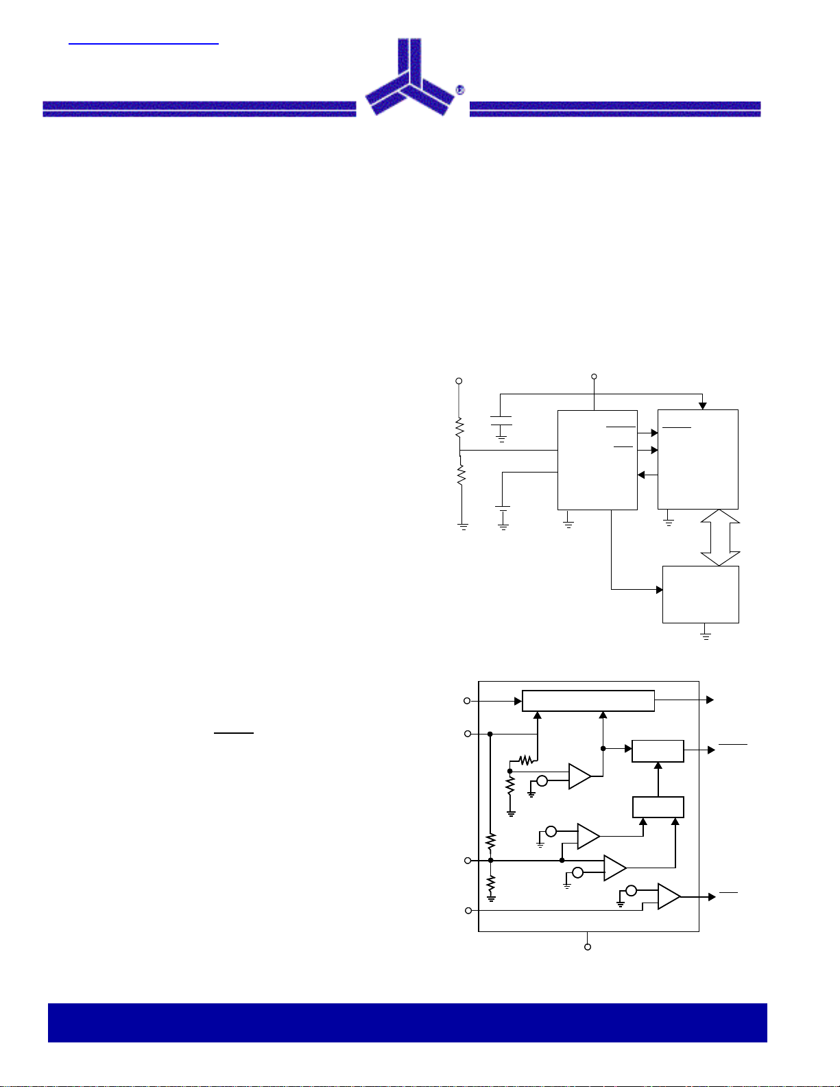
Typical Operating Circuit
Unregulated DC
R
R
0.1 µF
1
2
+
3.6 V
_
Lithium
Battery
PFI
V
BATT
GND
ASM690A
Regulated +5V
V
CC
RESET
PFO
WDI
V
OUT
Block Diagram
8
V
V
BATT
BATT
V
V
WDI
WDI
PFI
PFI
8
2
2
CC
CC
6
6
4
4
ASM690A, ASM692A, ASM802L, ASM802M, (ASM805L)
Battery-Switchover Circuit
Battery-Switchover Circuit
+
+
|+
|+
-
-
1.25V
1.25V
3.5V
3.5V
+
+
|+
|+
-
-
-
-
|+
|+
+
+
0.8V
0.8V
3
GND
Reset
Reset
Generator
Generator
Watchdog
Watchdog
Timer
Timer
1.25V
1.25V
|+
|+
RESET
NMI
I/O LINE
GND
V
CC
GND
-
-
+
+
V
CC
CMOS
RAM
1
1
7
7
5
5
BUS
V
V
OUT
OUT
RESET
RESET
(RESET)
(RESET)
PFO
PFO
Alliance Semiconductor
2575 Augustine Drive . Santa Clara, CA 95054 . Tel: 408.855.4900 . Fax: 408.855.4999 . www.alsc.com
Notice: The information in this document is subject to change without notice
Page 2
ASM690A / 692A
ASM802L / 802M
October 2003
rev 1.0
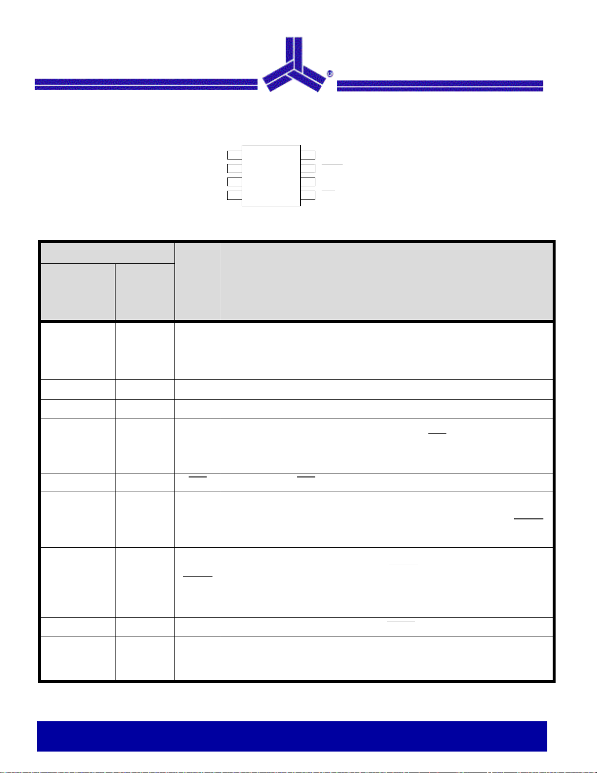
Pin Configuration
Pin Description
Pin Number
ASM690A /
ASM692A
ASM802L /
ASM802M
11
ASM805L
Plastic/CerDip/SO
V
OUT
V
CC
GND
PFI
Name Function
Voltage supply for RAM. When VCC is above the reset threshold, V
V
OUT
V
output will be connected to the backup supply at V
higher) through the MOS switch to provide continuous power to the CMOS RAM.
ASM690A
1
ASM692A
2
ASM802L
3
ASM802M
4
(ASM805L)
through a P-Channel MOS device. If VCC falls below the reset threshold, this
CC
V
8
BATT
7
RESET (RESET)
6
WDI
PFO
5
ASM805L
OUT
(or VCC, whichever is
BATT
connects to
22
3 3 GND Ground
44PFI
55PFO
66WDI
7 - RESET
- 7 RESET Active-HIGH reset output. The inverse of RESET
88
V
CC
V
BATT
+5V power supply input.
Power failure monitor input. PFI is connected to the internal power fail comparator
which is referenced to 1.25V. The power fail output (PFO
remains HIGH if PFI is above 1.25V. If this feature is unused, the PFI pin should be
connected to GND or V
Power-fail output. PFO is active LOW whenever the PFI pin is less than 1.25V.
Watchdog input. The WDI input monitors microprocessor activity. An internal timer
is reset with each transition of the WDI input. If the WDI is held HIGH or LOW for
longer than the watchdog timeout period, typically 1.6 seconds, RESET (or RESET
is asserted for the reset pulse width time, t
Active-LOW reset output. When triggered by VCC falling below the reset threshold
or by watchdog timer timeout, RESET (or RESET
width t
(4.65V in ASM690A / ASM802L and 4.4V in the ASM692A / ASM802L) and
remains low for 200ms after V
Auxiliary power or backup-battery input. V
function is not used. The input has about 40mV of hysteresis to prevent rapid toggling between V
, typically 200ms. It will remain low if VCC is below the reset threshold
RS
and V
CC
OUT
.
, of 140ms, minimum.
RS
rises above the reset threshold.
CC
should be connected to GND if the
BATT
.
BATT
) is active LOW but
)
) pulses low for the reset pulse
.
µP Power Supply Supervisor With Battery Backup Switch
Notice: The information in this document is subject to change without notice
2 of 13
Page 3

ASM690A / 692A
ASM802L / 802M
October 2003
rev 1.0
Detailed Description
It is important to initialize a microprocessor to a known state
in response to specific events that could create code
execution errors and “lock-up”. The reset output of these
supervisory circuits send a reset pulse to the microprocessor
in response to power-up, power-down/power-loss or a
watchdog time-out.
RESET/RESET
Power-up reset occurs when a rising V
threshold, V
output is asserted in the appropriate logic state for the
duration of t
200ms and is LOW for the ASM690A, ASM692A, ASM802
and HIGH for the ASM805L. Figure 1 shows the reset pin
timing.
Timing
reaches the reset
CC
, forcing a reset condition in which the reset
RT
. The reset pulse width, tRS, is typically around
RS
ASM805L
Application Information
Microprocessor Interface
The ASM690 has logic-LOW RESET output while the
ASM805 has an inverted logic-HIGH RESET output.
Microprocessors with bidirectional reset pins can pose a
problem when the supervisory circuit and the microprocessor
output pins attempt to go to opposite logic states. The
problem can be resolved by placing a 4.7kΩ resistor between
the RESET output and the microprocessor reset pin. This is
shown in Figure 2. Since the series resistor limits drive
capabilities, the reset signal to other devices should be
buffered.
Power-loss or “brown-out” reset occurs when V
the reset threshold resulting in a reset assertion for the
duration of t
V
is between VRT and 1.1V, the lowest VCC for which these
CC
devices can provide a guaranteed logic-low output. To ensure
logic inputs connected to the ASM690A / ASM692A/ASM802
RESET pin are in a known state when V
100kΩ pull-down resistor at RESET is needed: the logic-high
ASM805L will need a pull-up resistor to V
Watchdog Timer
A Watchdog time-out reset occurs when a logic “1” or logic
“0” is continuously applied to the WDI pin for more than 1.6
seconds. After the duration of the reset interval, the watchdog
timer starts a new 1.6 second timing interval; the
microprocessor must service the watchdog input by changing
states or by floating the WDI pin before this interval is
finished. If the WDI pin is held either HIGH or LOW, a reset
pulse will be triggered every 1.8 seconds (the 1.6 second
timing interval plus the reset pulse width t
RS. The reset signal remains asserted as long as
CC
CC
RS
dips below
CC
is under 1.1V, a
.
).
Figure 1: RESET/RESET Timing
V
CC
Power Supply
RESET
ASM690A
GND
Bi-directional I/O pin
4.7K
BUF
V
CC
Ω
RESET
GND
Buffered
RESET
Figure 2: Interfacing with bi-directional
microprocessor reset inputs
µP Power Supply Supervisor With Battery Backup Switch
Notice: The information in this document is subject to change without notice
3 of 13
Page 4
ASM690A / 692A
ASM802L / 802M
October 2003
rev 1.0
Watchdog Input
As discussed in the Reset section, the Watchdog input is
used to monitor microprocessor activity. It can be used to
insure that the microprocessor is in a continually responsive
state by requiring that the WDI pin be toggled every second.
If the WDI pin is not toggled within the 1.6 second window
(minimum t
the microprocessor to the initial start-up state. Pulses as
short as 50ns can be applied to the WDI pin. If this feature is
not used, the WDI pin should be open circuited or the logic
placed into a high-impedance state to allow the pin to float.
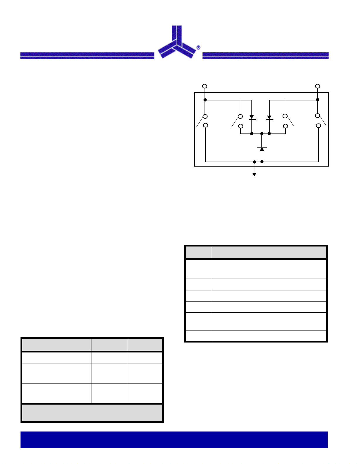
Backup-Battery Switchover
A power loss can be made less severe if the system RAM
contents are preserved. This is achieved in the ASM690/692/
802/805 by switching from the failed V
power source connected at V
reset threshold voltage (V
V
. The V
BATT
2Ω PMOS switch but a brown-out or loss of VCC will cause a
switchover to V
Although both conditions (VCC < VRT and VCC <V
occur for the switchover to V
switched back to V
the voltage at V
device diode (D1 in Figure 3) will be forward biased if V
exceeds VCC by more than a diode drop when VCC is
switched to V
V
be no greater than VRT +0.6V.
BATT
+ tRS), a reset pulse will be asserted to return
WD
to an alternate
CC
when VCC is less than the
BATT
< VRT), and VCC is less than
CC
pin is normally connected to VCC through a
OUT
by means of a 20Ω PMOS switch.
BATT
BATT
to occur, V
BATT
when VCC exceeds VRT irrespective of
CC
. It should be noted that an internal
BATT
. Because of this it is recommended that
OUT
OUT
will be
) must
BATT
ASM805L
V
BATT
D2
SW2
SW1
ASM690A
ASM692A
ASM802L
ASM802M
Figure 3: Internal device configuration of battery
switch-over function
Table 1. Pin Connections in Battery Backup Mode
Pin Connection
V
OUT
V
BATT
PFI Disabled
PFO Logic-LOW
RESET
Connected to V
switch
Connected to V
Logic-LOW (except on ASM805 where it is
HIGH)
D1
ASM805L
D3
V
OUT
through internal PMOS
BATT
OUT
V
SW3
CC
SW4
Condition SW1/SW2 SW3/SW4
V
> Reset Threshold
CC
V
< Reset Threshold
CC
V
> V
CC
BATT
< Reset Threshold
V
CC
V
< V
CC
BATT
ASM690A/802A/805L Reset Threshold = 4.65V
ASM692A /ASM802M Reset Threshold = 4.4V
open closed
open closed
closed open
µP Power Supply Supervisor With Battery Backup Switch
Notice: The information in this document is subject to change without notice
WDI Watchdog timer disabled
During the backup power mode, the internal circuitry of the
supervisory circuit draws power from the battery supply.
While V
and the current drawn by the device is typically 35µA. When
V
CC
switchover comparator, the PFI comparator and WDI
comparator will shut off, reducing the quiescent current drawn
by the IC to less than 1µA.
is still alive, the comparator circuits remain alive
CC
drops more than 1.1V below V
BATT
, the internal
4 of 13
Page 5

ASM690A / 692A
ASM802L / 802M
October 2003
rev 1.0
Backup Power Sources - Batteries
Battery voltage selection is important to insure that the
battery does not discharge through the parasitic device diode
D1 (see Figure 3) when V
VRT.
Table 2: Maximum Battery Voltages
Part Number MAXIMUM Battery Voltage
ASM690A 4.80
ASM802L 4.80
ASM805L 4.80
ASM692A 4.55
ASM802M 4.55
Although most batteries that meet the requirements of Tab le
2 are acceptable, lithium batteries are very effective backup
source due to their high-energy density and very low self-
discharge rates.
is less than V
CC
and VCC >
BATT
ASM805L
diode-resistor pair clamps the capacitor voltage at one diode
drop below V
5V for the ASM692A/802M or within ±10% of 5V for the
ASM690A/802L/805L to insure that the storage capacitor
does not achieve an over voltage state.
Note: SuperCap
+5V
+
Figure 4: Capacitor as a backup power source
. VCC itself should be regulated within ±5% of
CC
TM
is a trademark of Baknor Industries
D1
0.1F
V
CC
V
BATT
ASM692A
ASM802M
GND
V
OUT
RESET
(RESET)
SRAM
To
To µP
Battery replacement while Powered
Batteries can be replaced even when the device is in a
powered state as long as V
threshold voltage VRT. In the ASM devices, a floating V
pin will not cause a powersupply switchover as can occur in
some other supervisory circuits. If V
should be grounded.
Backup Power Sources - SuperCap™
Capacitor storage, with very high values of capacitance, can
be used as a back-up power source instead of batteries.
SuperCap
farad range. A 0.1 farad SuperCap™ would provide a useful
backup power source. Like the battery supply, it is important
that the capacitor voltage remain below the maximum
voltages shown in Table 2. Although the circuit of Figure 4
shows the most simple way to connect the SuperCap™, this
circuit cannot insure that an over voltage condition will not
occur since the capacitor will ultimately charge up to V
insure that an over voltage condition does not occur, the
circuit of Figure 5 is preferred. In this circuit configuration, the
™
are capacitors with capacities in the fractional
remains above the reset
CC
is not used, the pin
BATT
CC
BATT
. To
+5V
(RESET)
GND
V
OUT
RESET
V
D1
D2
100K
Figure 5: Capacitor as a backup power source
+
0.1F
Voltage clamped to 0.5V below V
CC
V
BATT
ASM692A
ASM802M
To SRAM
To µP
CC
µP Power Supply Supervisor With Battery Backup Switch
Notice: The information in this document is subject to change without notice
5 of 13
Page 6

ASM690A / 692A
ASM802L / 802M
October 2003
rev 1.0
Operation without a Backup Power Source
When operating without a back-up power source, the V
pin should be connected to GND and V
connected to VCC, since power source switchover will not
occur. Connecting V
due to the ON-resistance of the PMOS switch.
Power-Fail Comparator
The Power Fail feature is an independent voltage monitoring
function that can be used for any number of monitoring
activities. The PFI function can provide an early sensing of
power supply failure by sensing the voltage of the
unregulated DC ahead of the regulated supply sensing seen
by the backup-battery switchover circuitry. The PFI pin is
compared to a 1.25V internal reference. If the voltage at the
PFI pin is less than this reference voltage, the PFO
low. By sensing the voltage of the raw DC power supply, the
microprocessor system can prepare for imminent power-loss,
especially if the battery backup supply is not enabled. The
input voltage at the PFI pin results from a simple resistor
voltage divider as shown in Figure 6.
V
IN
to VCC eliminates the voltage drop
OUT
+5V
ASM690A
R1
V
CC
ASM692A
ASM802L
ASM802M
ASM805L
should be
OUT
BATT
pin goes
ASM805L
Power Fail Hysteresis
A noise margin can be added to the simple monitoring circuit
of Figure 6 by adding positive feedback from the PFO
The circuit of Figure 7 adds this positive “latching” effect by
means of an additional resistor R3 connected between PFO
and PFI which helps in pulling PFI in the direction of PFO and
eliminating an indecision at the trip point. Resistor R3 is
normally about 10 times higher in resistance than R2 to keep
the hysteresis band reasonable and should be larger than
10kΩ to avoid excessive loading on the PFO
calculations for the correct values of resistors to set the
hysteresis thresholds are given in Figure 7. A capacitor can
be added to offer additional noise rejection by low-pass
filtering.
V
IN
+5V
V
R
1
CC
ASM690A
ASM692A
ASM802L
PFI
R
2
C1*
R
3
ASM802M
ASM805L
PFO
GND
To µP
* Optional
pin.
pin. The
GND
2
1.25V>=
PFO
B
A
+5V
PFO
0V
5R
--------------------
R1R2+
PFI
R2
A
5R
--------------------
2
B
1.25V<=
R1R2+
Figure 6: Simple Voltage divider sets PFI trip point
µP Power Supply Supervisor With Battery Backup Switch
Notice: The information in this document is subject to change without notice
+5V
PFO
0V
V
V
51.25–
-------------------
+
L
TRIP
------------------------------------
=
V
H
⎛⎞
⎝⎠
1.25
----------
=
R
3
R
V
0V
TRIP
1.25
-------------------------
=
R
⎛⎞
2
--------------------
⎜⎟
R2R2+
⎝⎠
V
1.25–
L
-----------------------
R
1
Figure 7: Hysterisis Added To PFI Pin
V
H
1.25
||
R
2R3
------------------------------
R
||
+
1R2R3
2
6 of 13
Page 7

ASM690A / 692A
ASM802L / 802M
October 2003
rev 1.0
Monitoring Capabilities Of The Power-fail Input:
Although designed for power supply failure monitoring, the
PFI pin can be used for monitoring any voltage condition that
can be scaled by means of a resistive divider. An example is
the negative power supply monitor configured in Figure 8. In
this case a good negative supply will hold the PFI pin below
1.25V and the PFO
voltage declines, the voltage at the PFI pin will rise until it
exceeds 1.25V and the PFO
pin will be at logic “0”. As the negative
pin will go to logic “1”.
+5V
PFO
+5V
R
V-
ASM805L
ASM690A
V
CC
ASM692A
PFI
ASM802L
ASM802M
ASM805L
GND
PFO
V- = V
TRIP
1
R
2
0V
V
TRIP
V-
1.25 V
51.25–
-------------------
R
1
Figure 8: Using PFI To Monitor Negative Supply Voltage
–
-------------------------------
=
R
TRIP
2
0V
µP Power Supply Supervisor With Battery Backup Switch
Notice: The information in this document is subject to change without notice
7 of 13
Page 8

October 2003
rev 1.0
Absolute Maximum Ratings
Parameter Min Max Unit
Pin Terminal Voltage with Respect to Ground
ASM690A / 692A
ASM802L / 802M
ASM805L
V
CC
V
BATT
All other inputs * -0.3
Input Current at V
Input Current at V
Input Current at GND 20 mA
Output Current
V
OUT
All other inputs 20 mA
Rate of Rise: V
Continuous Power Dissipation
Plastic DIP (derate 9mW/°C above 70°C) 800 mW
SO (derate 5.9mW/°C above 70°C) 500 mW
CerDIP (derate 8mW/°C above 70°C) 650 mW
Operating Temperature Range (C Devices) 0 70 °C
CC
BATT
BATT
and V
CC
-0.3 6.0 V
-0.3 6.0 V
V
+ 0.3
CC
200 mA
50 mA
Short circuit protected
100 V/µs
V
Operating Temperature Range (E Devices) -40 85 °C
Storage Temperature Range -65 160 °C
Lead Temperature Soldering, (10 sec) 300 °C
* The input voltage limits on PFI and WDI may be exceeded if the current is limited to less than 10mA
Note: These are stress ratings only and functional operation is not implied. Exposure to absolute maximum ratings for prolonged time periods
may affect device reliability.
µP Power Supply Supervisor With Battery Backup Switch
Notice: The information in this document is subject to change without notice
8 of 13
Page 9

ASM690A / 692A
ASM802L / 802M
October 2003
rev 1.0
Electrical Characteristics:
Unless other wise noted, VCC = 4.75V to 5.5V for the ASM690A / ASM802L / ASM805L and VCC = 4.5V to 5.5V for the ASM692A / ASM802M;
V
= 2.8V; and TA = T
BATT
Parameter Symbol Conditions Min Typ Max Unit
, V
BATT
Voltage
V
CC
Range (Note 1)
MIN
to T
.
MAX
ASM69_AC, ASM802_C 1.1 5.5
ASM69_AE, ASM80__E 1.1 5.5
ASM805L
VASM805LC 1.1 5.5
Supply Current
Excluding I
I
SUPPLY
Backup Mode
(Excluding I
V
BATT
Current (Note 2)
V
OUT
V
OUT
Backup Mode
Battery Switch
Threshold,
V
CC
Battery Switch over
Hysteresis
OUT
in Battery
OUT
Standby
Output
in Battery
to V
BATT
)
I
S
ASM69_AC, ASM80__E 35 100
ASM69_AC, ASM802_C 35 100
T
= 25°C
A
V
= 0V, V
CC
5.5V>V
CC>VBATT
= 5mA
I
OUT
= 50mA VCC-0.25 VCC-0.10
I
OUT
I
=250µA, VCC < V
OUT
VCC < V
ASM690A/802L/805L 4.50 4.65 4.75
RT
BATT
=2.8V
-0.2V
TA = T
TA = 25°C
T
A
-0.2V V
BATT
Power Up
Power Down
= T
MIN
MIN
to T
to T
MAX
MAX
-0.1
-1.0
V
CC
0.025
BATT
-
-0.1 V
-0.010
V
CC
-0.001
BATT
20
-20
40 mV
1.0
5.0
0.02
0.02
µA
µA
µA
V
V
mV
ASM692A, ASM802M 4.25 4.40 4.50
Reset Threshold
V
RT
ASM802L, T
= 25°C, VCC falling
A
ASM802M, T
Notes:
1. If V
2. Battery charging-current is “-”. Battery discharge current is “+”.
3. WDI is guaranteed to be in an intermediate level state if WDI is floating and V
input impedance is 50 kΩ. WDI is biased to 0.3V
CC
or V
is 0V, the other must be greater than 2.0V.
BATT
µP Power Supply Supervisor With Battery Backup Switch
Notice: The information in this document is subject to change without notice
=25°C, VCC falling
A
.
CC
4.55 4.70
4.30 4.45
is within the operating voltage range. WDI
CC
V
9 of 13
Page 10

ASM690A / 692A
ASM802L / 802M
October 2003
rev 1.0
Parameter Symbol Conditions Min Typ Max Unit
ASM805L
Reset Threshold
Hysteresis
Reset Pulse Width
Reset Output Voltage
Watchdog Timeout
WDI Pulse Width
WDI Input Current
t
t
t
RS
WD
WP
40 mV
140 200 280 ms
I
SOURCE
I
SINK
ASM69_AC, ASM802_C, V
I
SINK
ASM69_AE, ASM802_E, V
I
SINK
ASM805LC, I
ASM805LE, I
ASM805L, I
ASM805L, I
VIL = 0.4V, VIH = 0.8V
WDI = V
WDI = 0V -150 -50 µA
= 800µA VCC - 1.5
= 3.2mA
=1.0V,
CC
=50µA
=1.2V,
CC
=100µA
SOURCE
SOURCE
SOURCE
SINK
CC
=4µA, VCC = 1.1V
=4µA, VCC = 1.2V
=800µA VCC - 1.5
=3.2mA
CC
0.4
0.3
0.3
0.8
0.9
0.4
1.00 1.60 2.25 sec
50 ns
50 150 µA
V
WDI Input Thresh-
V
old
(Note 3)
PFI Input Threshold
PFI Input Current -25 0.01 25 nA
PFO Output Voltage
Notes:
1. If V
2. Battery charging-current is “-”. Battery discharge current is “+”.
3. WDI is guaranteed to be in an intermediate level state if WDI is floating and V
input impedance is 50 kΩ. WDI is biased to 0.3V
CC
or V
is 0V, the other must be greater than 2.0V.
BATT
= 5V, Logic LOW
CC
ASM69_A,ASM805L, V
ASM802_C/E, V
I
SOURCE
I
SINK
= 800µA VCC - 1.5
= 3.2mA
CC
= 5V
.
CC
CC
= 5V
0.8 V
1.20 1.25 1.30
1.225 1.250 1.275
0.4
is within the operating voltage range. WDI
CC
V
V
10 of 13
µP Power Supply Supervisor With Battery Backup Switch
Notice: The information in this document is subject to change without notice
Page 11

ASM690A / 692A
ASM802L / 802M
October 2003
rev 1.0
Plastic DIP (8-Pin)
CerDIP (8-Pin)
SO (8-Pin)
ASM805L
Package Information
Inches Millimeters
Min Max Min Max
Plastic DIP (8-Pin) *
A - 0.210 - 5.33
A1 0.015 - 0.38 -
A2 0.115 0.195 2.92 4.95
b 0.014 0.022 0.36 0.56
b2 0.045 0.070 1.14 1.78
b3 0.030 0.045 0.80 1.14
D 0.355 0.400 0.80 1.14
D1 0.005 - 0.13 -
E 0.300 0.325 7.62 8.26
E1 0.240 0.280 6.10 7.11
e 0.100 - 2.54
eA 0.300 - 7.62
eB - 0.430 - 10.92
eC - 0.060
L 0.115 0.150 2.92 3.81
CerDIP (8-Pin)
A - 0.200 - 5.08
A1 0.015 0.070 0.38 1.78
b 0.014 0.023 0.36 0.58
B2 0.038 0.065 0.97 1.65
C 0.008 0.015 0.20 0.38
D - 0.405 - 10.29
D1 0.005 - 0.13 -
E 0.290 0.320 7.37 8.13
E1 0.220 0.310 5.59 7.87
e 0.100 2.54
L 0.125 0.200 3.18 5.08
SO (8-Pin) **
A 0.053 0.069 1.35 1.75
A1 0.004 0.010 0.10 0.25
B 0.013 0.020 0.33 0.51
C 0.007 0.010 0.19 0.25
e 0.050 1.27
E 0.150 0.157 3.80 4.00
H 0.228 0.244 5.80 6.20
L 0.016 0.050 0.40 1.27
D 0.189 0.197 4.80 5.00
µP Power Supply Supervisor With Battery Backup Switch
Notice: The information in this document is subject to change without notice
11 of 13
Page 12

ASM690A / 692A
ASM802L / 802M
October 2003
rev 1.0
Ordering Information
Part Number Reset Threshold (V) Temperature Range (°C) Pins-Package
ASM690A
ASM690ACPA 4.5 TO 4.75 0 TO +70 8-Plastic DIP
ASM690ACSA 4.5 TO 4.75 0 TO +70 8-SO
ASM690AC/D 4.5 TO 4.75 25 DICE
ASM690AEPA -40 TO +85 8-Plastic DIP
ASM690AESA 4.5 TO 4.75 -40 TO +85 8-SO
ASM690AMJA 4.5 TO 4.75 Contact Factory 8-Cer DIP
ASM692A
ASM692ACPA 4.25 TO 4.50 0 TO +70 8-Plastic DIP
ASM805L
ASM692ACSA 4.25 TO 4.50 0 TO +70 8-SO
ASM692AC/D 4.25 TO 4.50 25 DICE
ASM692AEPA 4.25 TO 4.50 -40 TO +85 8-Plastic DIP
ASM692AESA 4.25 TO 4.50 -40 TO +85 8-SO
ASM692AMJA 4.25 TO 4.50 Contact Factory 8-Cer DIP
ASM802L
ASM802LCPA 4.5 TO 4.75 0 TO +70 8-Plastic DIP
ASM802LCSA 4.5 TO 4.75 0 TO +70 8-SO
ASM802LAEPA 4.5 TO 4.75 -40 TO +85 8-Plastic DIP
ASM802LESA 4.5 TO 4.75 -40 TO +85 8-SO
ASM802M
ASM802MCPA 4.25 TO 4.50 0 TO +70 8-Plastic DIP
ASM802MCSA 4.25 TO 4.50 0 TO +70 8-SO
ASM802MEPA 4.25 TO 4.50 -40 TO +85 8-Plastic DIP
ASM802MESA 4.25 TO 4.50 -40 TO +85 8-SO
ASM805L
ASM805LCPA 4.5 TO 4.75 0 TO +70 8-Plastic DIP
ASM805LCSA 4.5 TO 4.75 0 TO +70 8-SO
ASM805LC/D 4.5 TO 4.75 25 DICE
ASM805LEPA 4.5 TO 4.75 -40 TO +85 8-Plastic DIP
ASM805LESA 4.5 TO 4.75 -40 TO +85 8-SO
ASM805LMJA 4.5 TO 4.75 Contact Factory 8-Cer DIP
µP Power Supply Supervisor With Battery Backup Switch
Notice: The information in this document is subject to change without notice
12 of 13
Page 13

October 2003
rev 1.0
ASM690A / 692A
ASM802L / 802M
ASM805L
Alliance Semiconductor Corporation
2575, Augustine Drive,
Santa Clara, CA 95054
Tel: 408 - 855 - 4900
Fax: 408 - 855 - 4999
www.alsc.com
© Copyright 2003 Alliance Semiconductor Corporation. All rights reserved. Our three-point logo, our name and Intelliwatt are trademarks or
registered trademarks of Alliance. All other brand and product names may be the trademarks of their respective companies. Alliance reserves the
right to make changes to this document and its products at any time without notice. Alliance assumes no responsibility for any errors that may
appear in this document. The data contained herein represents Alliance's best data and/or estimates at the time of issuance. Alliance reserves the
right to change or correct this data at any time, without notice. If the product described herein is under development, significant changes to these
specifications are possible. The information in this product data sheet is intended to be general descriptive information for potential customers and
users, and is not intended to operate as, or provide, any guarantee or warrantee to any user or customer. Alliance does not assume any responsibility
or liability arising out of the application or use of any product described herein, and disclaims any express or implied warranties related to the sale
and/or use of Alliance products including liability or warranties related to fitness for a particular purpose, merchantability, or infringement of any
intellectual property rights, except as express agreed to in Alliance's Terms and Conditions of Sale (which are available from Alliance). All sales of
Alliance products are made exclusively according to Alliance's Terms and Conditions of Sale. The purchase of products from Alliance does not
convey a license under any patent rights, copyrights; mask works rights, trademarks, or any other intellectual property rights of Alliance or third
parties. Alliance does not authorize its products for use as critical components in life-supporting systems where a malfunction or failure may
reasonably be expected to result in significant injury to the user, and the inclusion of Alliance products in such life-supporting systems implies that
the manufacturer assumes all risk of such use and agrees to indemnify Alliance against all claims arising from such use.
Copyright © Alliance Semiconductor
All Rights Reserved
Part Number: ASM690A / 692A
ASM802L / 802M
ASM805L
Document Version: 1.0
 Loading...