

Page 1
/
(
)
查询ASM5I23S04A-1H-08-SR供应商
September 2005 ASM5P23S04A
rev 1.3
3.3V ‘SpreadTrak’ Zero Delay Buffer
Features
Zero input - output propagation delay, adjustable
by capacitive load on FBK input.
Multiple configurations - Refer “ASM5P23S04A
Configurations Table”.
Input frequency range: 15MHz to 133MHz
Multiple low-skew outputs.
Output-output skew less than 200pS.
Device-device skew less than 500pS.
Two banks of two outputs each.
Less than 200pS Cycle-to-cycle jitter
(-1, -1H, -2, -2H).
Available in space saving, 8 pin 150-mil SOIC
package.
3.3V operation.
Advanced 0.35µ CMOS technology.
Industrial temperature available.
‘SpreadTrak’.
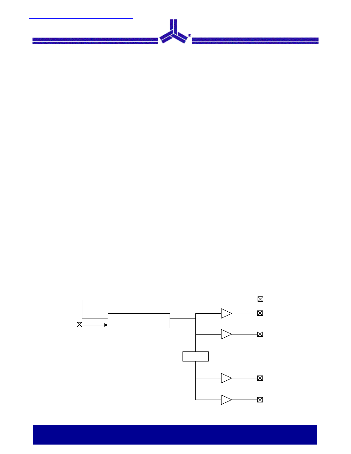
Functional Description
ASM5P23S04A is a versatile, 3.3V zero-delay buffer
designed to distribute high-speed clocks in PC,
workstation, datacom, telecom and other high-performance
applications. It is available in a 8 pin package. The part has
an on-chip PLL, which locks to an input clock, presented on
Block Diagram
the REF pin. The PLL feedback is required to be driven to
FBK pin, and can be obtained from one of the outputs. The
input-to-output propagation delay is guaranteed to be less
than 250pS, and the output-to-output skew is guaranteed to
be less than 200pS.
The ASM5P23S04A has two banks of two outputs each.
Multiple ASM5P23S04A devices can accept the same input
clock and distribute it. In this case the skew between the
outputs of the two devices is guaranteed to be less than
500pS.
The ASM5P23S04A is available in two different
configurations (Refer “ASM5P23S04A Configurations
Table). The ASM5P23S04A-1 is the base part, where the
output frequencies equal the reference if there is no
counter in the feedback path. The ASM5P23S04A-1H is
the high-drive version of the -1 and the rise and fall times
on this device are much faster.
The ASM5P23S04A-2 allows the user to obtain REF and
1/2X or 2X frequencies on each output bank. The exact
configuration and output frequencies depend on which
output drives the feedback pin.
FBK
CLKA1
REF
PLL
Alliance Semiconductor
2
Extra Divider
CLKA2
-2
CLKB1
CLKB2
2575 Augustine Drive • Santa Clara, CA • Tel: 408.855.4900 • Fax: 408.855.4999 • www.alsc.com
Notice: The information in this document is subject to change without notice.
Page 2
September 2005
ASM5P23S04A
rev 1.3
ASM5P23S04A Configurations
Device Feedback From Bank A Frequency Bank B Frequency
ASM5P23S04A-1 Bank A or Bank B Reference Reference
ASM5P23S04A-1H Bank A or Bank B Reference Reference
ASM5P23S04A-2 Bank A Reference Reference /2
ASM5P23S04A-2 Bank B 2 X Reference Reference
ASM5P23S04A-2H Bank A Reference Reference/2
ASM5P23S04A-2H Bank B 2 X Reference Reference
‘SpreadTrak’
Many systems being designed now utilize a technology
called Spread Spectrum Frequency Timing Generation.
ASM5P23S04A is designed so as not to filter off the
Spread Spectrum feature of the Reference Input,
assuming it exists. When a zero delay buffer is not
designed to pass the Spread Spectrum feature through,
the result is a significant amount of tracking skew which
may cause problems in the systems requiring
synchronization.
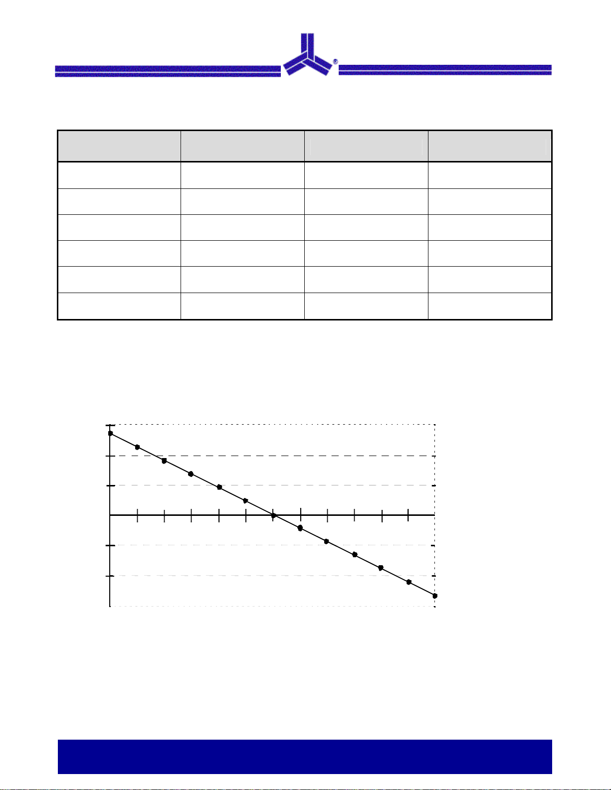
1500
1000
500
0
-30
-25
-20 -15 -10 -5
-500
-1000
REF-Input to CLKA/CLKB Delay (ps)
-1500
REF Input to CLKA/CLKB Delay Vs Difference in Loading between FBK pin and CLKA/CLKB pins
Output Load Difference: FBK Load - CLKA/CLKB Load (pF)
0
5
10 15 20 25
30
3.3 Zero ‘SpreadTrak’ Delay Buffer 2 of 15
Notice: The information in this document is subject to change without notice.
Page 3
September 2005
ASM5P23S04A
rev 1.3
Zero Delay and Skew Control
For applications requiring zero input-output delay, all
outputs must be equally loaded. To close the feedback loop
of ASM5P23S04A, the FBK pin can be driven from any of
the four available output pins. The output driving the FBK
pin will be driving a total load of 7pF plus any additional
load that it drives. The relative loading of this output (with
respect to the remaining outputs) can adjust the input
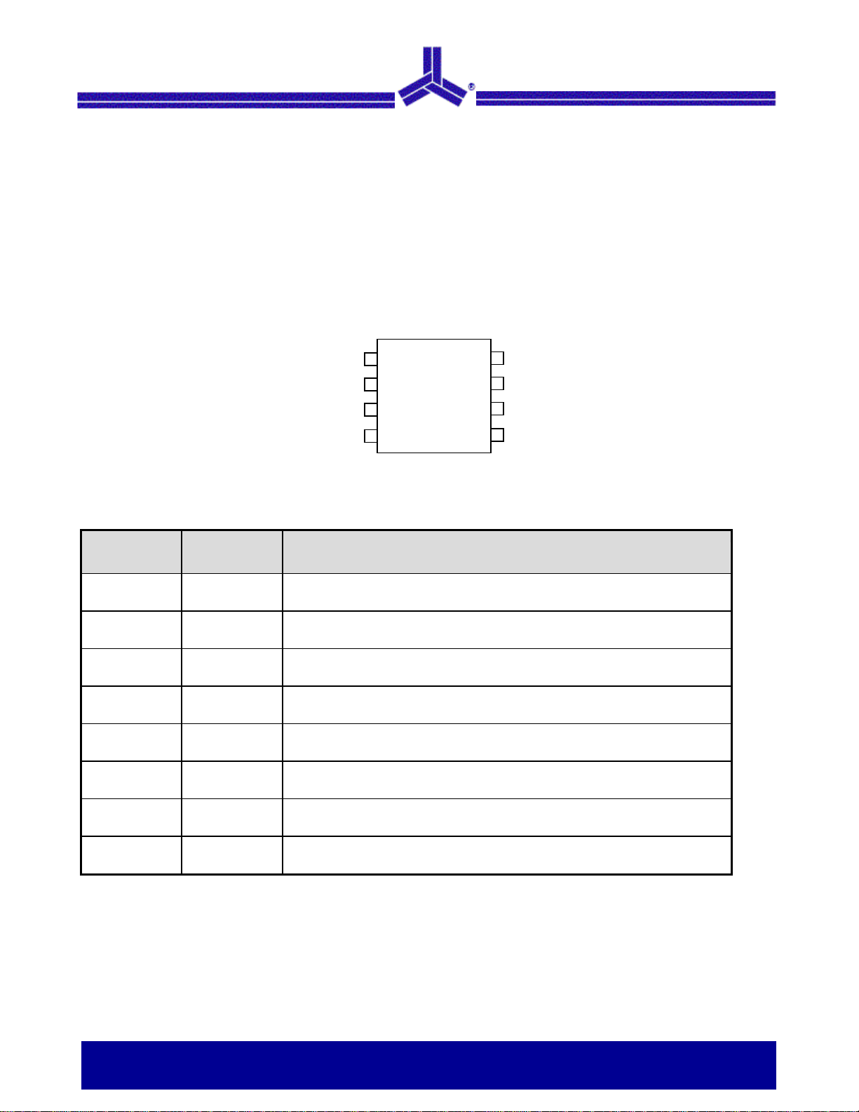
Pin Configuration
GND
1
2
ASM5P23S04A
3
4
Pin Description for ASM5P23S04A
REF
CLKA1
CLKA2
output delay. This is shown in the above graph. For
applications requiring zero input-output delay, all outputs
including the one providing feedback should be equally
loaded. If input-output delay adjustments are required, use
the above graph to calculate loading differences between
the feedback output and remaining outputs. For zero
output-output skew, be sure to load outputs equally.
8FBK
7
V
DD
CLKB2
6
5
CLKB1
Pin # Pin Name Description
1 REF1 Input reference frequency, 5V tolerant input
2 CLKA12 Buffered clock output, bank A
3 CLKA22 Buffered clock output, bank A
4 GND Ground
5 CLKB12 Buffered clock output, bank B
6 CLKB2
7 VDD 3.3V supply
8 FBK PLL feedback input
Notes:
1. Weak pull-down.
2. Weak pull-down on all outputs.
2
Buffered clock output, bank B
3.3 Zero ‘SpreadTrak’ Delay Buffer 3 of 15
Notice: The information in this document is subject to change without notice.
Page 4

September 2005
ASM5P23S04A
rev 1.3
Absolute Maximum Ratings
Parameter Min Max Unit
Supply Voltage to Ground Potential -0.5 +7.0 V
DC Input Voltage (Except REF) -0.5 VDD + 0.5 V
DC Input Voltage (REF) -0.5 7 V
Storage Temperature -65 +150 °C
Max. Soldering Temperature (10 sec) 260 °C
Junction Temperature 150 °C
Static Discharge Voltage
(As per JEDEC STD22- A114-B)
>2000 V
Note: These are stress ratings only and functional usage is not implied. Exposure to absolute maximum ratings for prolonged periods can affect device
reliability.
Operating Conditions for ASM5P23S04A Commercial Temperature Devices
Parameter Description Min Max Unit
VDD Supply Voltage 3.0 3.6 V
TA Operating Temperature (Ambient Temperature) 0 70 °C
CL Load Capacitance, below 100MHz 30 pF
CL Load Capacitance, from 100MHz to 133MHz 15 pF
CIN Input Capacitance3 7 pF
Note:
3. Applies to both Ref Clock and FBK.
3.3 Zero ‘SpreadTrak’ Delay Buffer 4 of 15
Notice: The information in this document is subject to change without notice.
Page 5
September 2005
ASM5P23S04A
rev 1.3
Electrical Characteristics for ASM5P23S04A Commercial Temperature Devices
Parameter Description Test Conditions Min Max Unit
VIL Input LOW Voltage 0.8 V
VIH Input HIGH Voltage 2.0 V
IIL Input LOW Current VIN = 0V 50.0 µA
IIH Input HIGH Current VIN = VDD 100.0 µA
I
= 8mA (-1, -2)
VOL Output LOW Voltage 4
VOH Output HIGH Voltage 4
OL
I
= 12mA (-1H, -2H)
OH
I
= -8mA (-1, -2)
OL
IOH = -12mA (-1H, -2H)
0.4 V
2.4 V
Unloaded outputs 100MHz REF,
Select inputs at V
IDD Supply Current
Note:
4. Parameter is guaranteed by design and characterization. Not 100% tested in production.
Unloaded outputs, 66MHz REF
(-1, -2)
Unloaded outputs, 33MHz REF
(-1, -2)
or GND
DD
45.0
mA
32.0
18.0
3.3 Zero ‘SpreadTrak’ Delay Buffer 5 of 15
Notice: The information in this document is subject to change without notice.
Page 6

September 2005
ASM5P23S04A
rev 1.3
Switching Characteristics for ASM5P23S04A Commercial Temperature Devices
Parameter Description Test Conditions Min Typ Max Unit
1/t1 Output Frequency 30pF load, All devices 15 100 MHz
1/t1 Output Frequency 15pF load, -1H, -2H devices 15 133 MHz
1/t1 Output Frequency 15pF load, -1, -2 devices 15 133 MHz
t3
t3
t3
t4
t4
t4
Duty Cycle
(-1, -2, -1H, -2H)
Duty Cycle
(-1, -2,-1H, -2H)
Output Rise Time
(-1, -2)
Output Rise Time
(-1, -2)
Output Rise Time
(-1H, -2H)
Output Fall Time
(-1, -2)
Output Fall Time
(-1, -2)
Output Fall Time
(-1H, -2H)
5
= (t2 / t1) * 100
5
= (t2 / t1) * 100
5
5
5
5
5
5
Measured at 1.4V, F
30pF load
Measured at 1.4V, F
15 pF load
= 66.66MHz
OUT
= <50MHz
OUT
Measured between 0.8V and 2.0V
30pF load
Measured between 0.8V and 2.0V
15pF load
Measured between 0.8V and 2.0V
30pF load
Measured between 2.0V and 0.8V
30pF load
Measured between 2.0V and 0.8V
15pF load
Measured between 2.0V and 0.8V
30pF load
40.0 50.0 60.0 %
45.0 50.0 55.0 %
2.20 nS
1.50 nS
1.50 nS
2.20 nS
1.50 nS
1.25 nS
Output-to-output skew on same bank (-1, -2) 5 All outputs equally loaded 200
t5
Output-to-output skew (-1H, -2H) All outputs equally loaded 200
Output bank A -to- output bank B skew (-1, -2H) All outputs equally loaded 200
Output bank A to output bank B skew (-2) All outputs equally loaded 400
t6 Delay, REF Rising Edge to FBK Rising Edge 5 Measured at VDD /2 0 ±250 pS
t7 Device-to-Device Skew
t8 Output Slew Rate5
5
Measured at VDD/2 on the FBK pins of the device 0 500 pS
Measured between 0.8V and 2.0V using
Test Circuit #2
1 V/nS
Measured at 66.67MHz, loaded outputs, 15pF load 175
Cycle-to-cycle jitter
(-1, -1H, -2H)
Cycle-to-cycle jitter
(-2)
PLL Lock Time 5
t
LOCK
tJ
tJ
5
5
Measured at 66.67MHz, loaded outputs,
30pF load
Measured at 133MHz, loaded outputs,
15pF load
200
100
Measured at 66.67MHz, loaded outputs, 30pF load 400
Measured at 66.67MHz, loaded outputs,
15pF load
Stable power supply, valid clock presented on REF
and FBK pins
375
1.0 mS
Note:
5. Parameter is guaranteed by design and characterization. Not 100% tested in production.
pS
pS
pS
3.3 Zero ‘SpreadTrak’ Delay Buffer 6 of 15
Notice: The information in this document is subject to change without notice.
Page 7

September 2005
ASM5P23S04A
rev 1.3
Operating Conditions for ASM5I23S04A Industrial Temperature Devices
Parameter Description Min Max Unit
VDD Supply Voltage 3.0 3.6 V
TA Operating Temperature (Ambient Temperature) -40 85 °C
CL Load Capacitance, below 100MHz 30 pF
CL Load Capacitance, from 100MHz to 133MHz 15 pF
CIN Input Capacitance6 7 pF
Note:
6. Applies to both Ref Clock and FBK.
Electrical Characteristics for ASM5I23S04A Industrial Temperature Devices
Parameter Description Test Conditions Min Max Unit
VIL Input LOW Voltage 0.8 V
VIH Input HIGH Voltage 2.0 V
IIL Input LOW Current VIN = 0V 50.0 µA
IIH Input HIGH Current VIN = VDD 100.0 µA
= 8mA (-1, -2)
I
VOL Output LOW Voltage 7
VOH Output HIGH Voltage
IDD Supply Current
7
OL
I
= 12mA (-1H, -2H)
OH
IOL = -8mA (-1, -2)
I
= -12mA (-1H, -2H)
OH
Unloaded outputs 100MHz REF, Select inputs
or GND
at V
DD
Unloaded outputs, 66MHz REF (-1, -2) 35.0
0.4 V
2.4 V
45.0
mA
Unloaded outputs, 33MHz REF (-1, -2) 20.0
Note:
7. Parameter is guaranteed by design and characterization. Not 100% tested in production.
3.3 Zero ‘SpreadTrak’ Delay Buffer 7 of 15
Notice: The information in this document is subject to change without notice.
Page 8

September 2005
ASM5P23S04A
rev 1.3
Switching Characteristics for ASM5I23S04A Industrial Temperature Devices
Parameter Description Test Conditions Min Typ Max Unit
t1 Output Frequency 30pF load, All devices 15 100 MHz
t1 Output Frequency 15pF load, -1H, -2H devices 15 133 MHz
t1 Output Frequency 15pF load, -1 and -2 devices 15 133 MHz
t3
t3
t3
t4
t4
t4
Duty Cycle
(-1, -2, -1H, -2H)
Duty Cycle
(-1, -2, -1H, -2H)
Output Rise Time
(-1, -2)
Output Rise Time
(-1, -2)
Output Rise Time
(-1H, -2H)
Output Fall Time
(-1, -2)
Output Fall Time
(-1, -2)
Output Fall Time
(-1H, -2H)
8
= (t2 / t1) * 100
8
= (t2 / t1) * 100
8
8
8
8
8
8
Measured at 1.4V, F
30pF load
Measured at 1.4V, F
15pF load
= <66.66MHz
OUT
= <50MHz
OUT
Measured between 0.8V and 2.0V
30pF load
Measured between 0.8V and 2.0V
15pF load
Measured between 0.8V and 2.0V
30pF load
Measured between 2.0V and 0.8V
30pF load
Measured between 2.0V and 0.8V
15pF load
Measured between 2.0V and 0.8V
30pF load
40.0 50.0 60.0 %
45.0 50.0 55.0 %
2.50 nS
1.50 nS
1.50 nS
2.50 nS
1.50 nS
1.25 nS
Output-to-output skew on same bank (-1, -2) 8 All outputs equally loaded 200
t5
Output-to-output skew (-1H, -2H) All outputs equally loaded 200
Output bank A -to- output bank B skew (-1, -2H) All outputs equally loaded 200
Output bank A -to- output bank B skew (-2) All outputs equally loaded 400
t6 Delay, REF Rising Edge to FBK Rising Edge 8 Measured at VDD /2 0 ±250 pS
t7 Device-to-Device Skew
t8 Output Slew Rate8
Cycle-to-cycle jitter
(-1, -1H, -2H)
Cycle-to-cycle jitter
(-2)
PLL Lock Time 8
t
LOCK
tJ
tJ
8
Measured at VDD/2 on the FBK pins of the device 0 500 pS
Measured between 0.8V and 2.0V using
Test Circuit #2
Measured at 66.67MHz, loaded outputs,
15pF load
8
Measured at 66.67MHz, loaded outputs,
30pF load
Measured at 133MHz, loaded outputs,
15pF load
8
Measured at 66.67MHz, loaded outputs, 30pF load 400
Measured at 66.67 MHz, loaded outputs,
15pF load
Stable power supply, valid clock presented on REF
and FBK pins
1 V/nS
180
200
100
380
1.0 mS
Note: 8. Parameter is guaranteed by design and characterization. Not 100% tested in production.
pS
pS
pS
3.3 Zero ‘SpreadTrak’ Delay Buffer 8 of 15
Notice: The information in this document is subject to change without notice.
Page 9

September 2005
ASM5P23S04A
rev 1.3
Switching Waveforms
Duty Cycle Timing
t
2
1.4 V
All Outputs Rise/Fall Time
2.0 V
OUTPUT
0.8 V
t
3
Output - Output Skew
1.4 V
t
t
1
4
2.0 V
0.8 V
1.4 V
3.3 V
0 V
OUTPUT1
OUTPUT2
1.4 V
1.4 V
t
5
Input - Output Propagation Delay
/2
V
DD
INPUT
/2
V
DD
OUTPUT
t
6
Device - Device Skew
/2
V
DD
CLKOUT, Device 1
V
CLKOUT, Device 2
t
7
DD
/2
3.3 Zero ‘SpreadTrak’ Delay Buffer 9 of 15
Notice: The information in this document is subject to change without notice.
Page 10

September 2005
rev 1.3
Test Circuits
0.1uF
0.1uF
ASM5P23S04A
TEST CIRCUIT # 1
VDD
GND
V
DD
GND
OUTPUT
CLKOUT
C
LOAD
0.1uF
0.1uF
For parameter t
TEST CIRCUIT # 2
VDD
OUTPUT
V
DD
GND
(output skew rate)
8
GND
1KΩ
1KΩ
10pF
3.3 Zero ‘SpreadTrak’ Delay Buffer 10 of 15
Notice: The information in this document is subject to change without notice.
Page 11

C
September 2005
ASM5P23S04A
rev 1.3
Package Information
8-lead (150-mil) SOIC Package
H
E
D
A2
A
e
B
A1
D
θ
L
Dimensions
Symbol
Inches
Millimeters
Min Max Min Max
A1 0.004 0.010 0.10 0.25
A 0.053 0.069 1.35 1.75
A2 0.049 0.059 1.25 1.50
B 0.012 0.020 0.31 0.51
C 0.007 0.010 0.18 0.25
D 0.193 BSC 4.90 BSC
E 0.154 BSC 3.91 BSC
e 0.050 BSC 1.27 BSC
H 0.236 BSC 6.00 BSC
L 0.016 0.050 0.41 1.27
θ 0° 8° 0° 8°
3.3 Zero ‘SpreadTrak’ Delay Buffer 11 of 15
Notice: The information in this document is subject to change without notice.
Page 12

September 2005
ASM5P23S04A
rev 1.3
Ordering Codes
Ordering Code Marking Package Type
ASM5P23S04A-1-08-SR 5P23S04A-1 8-pin 150-mil SOIC-TAPE & REEL Commercial
ASM5P23S04A-1-08-ST 5P23S04A-1 8-pin 150-mil SOIC-TUBE Commercial
ASM5I23S04A-1-08-SR 5I23S04A-1 8-pin 150-mil SOIC-TAPE & REEL Industrial
ASM5I23S04A-1-08-ST 5I23S04A-1 8-pin 150-mil SOIC-TUBE Industrial
ASM5P23S04A-1H-08-SR 5P23S04A-1H 8-pin 150-mil SOIC-TAPE & REEL Commercial
ASM5P23S04A-1H-08-ST 5P23S04A-1H 8-pin 150-mil SOIC-TUBE Commercial
Operating
Range
ASM5I23S04A-1H-08-SR 5I23S04A-1H 8-pin 150-mil SOIC-TAPE & REEL Industrial
ASM5I23S04A-1H-08-ST 5I23S04A-1H 8-pin 150-mil SOIC-TUBE Industrial
ASM5P23S04A-2-08-SR 5P23S04A-2 8-pin 150-mil SOIC-TAPE & REEL Commercial
ASM5P23S04A-2-08-ST 5P23S04A-2 8-pin 150-mil SOIC-TUBE Commercial
ASM5I23S04A-2-08-SR 5I23S04A-2 8-pin 150-mil SOIC-TAPE & REEL Industrial
ASM5I23S04A-2-08-ST 5I23S04A-2 8-pin 150-mil SOIC-TUBE Industrial
ASM5P23S04A-2H-08-SR 5P23S04A-2H 8-pin 150-mil SOIC-TAPE & REEL Commercial
ASM5P23S04A-2H-08-ST 5P23S04A-2H 8-pin 150-mil SOIC-TUBE Commercial
ASM5I23S04A-2H-08-SR 5I23S04A-2H 8-pin 150-mil SOIC-TAPE & REEL Industrial
ASM5I23S04A-2H-08-ST 5I23S04A-2H 8-pin 150-mil SOIC-TUBE Industrial
ASM5P23S04AF-1-08-SR 5P23S04AF-1 8-pin 150-mil SOIC-TAPE & REEL, Pb free Commercial
ASM5P23S04AF-1-08-ST 5P23S04AF-1 8-pin 150-mil SOIC-TUBE, Pb free Commercial
ASM5I23S04AF-1-08-SR 5I23S04AF-1 8-pin 150-mil SOIC-TAPE & REEL, Pb free Industrial
ASM5I23S04AF-1-08-ST 5I23S04AF-1 8-pin 150-mil SOIC-TUBE, Pb free Industrial
3.3 Zero ‘SpreadTrak’ Delay Buffer 12 of 15
Notice: The information in this document is subject to change without notice.
Page 13

September 2005
ASM5P23S04A
rev 1.3
Ordering Codes (cont’d)
Ordering Code Marking Package Type
ASM5P23S04AF-1H-08-SR 5P23S04AF-1H 8-pin 150-mil SOIC-TAPE & REEL, Pb free Commercial
ASM5P23S04AF-1H-08-ST 5P23S04AF-1H 8-pin 150-mil SOIC-TUBE, Pb free Commercial
ASM5I23S04AF-1H-08-SR 5I23S04AF-1H 8-pin 150-mil SOIC-TAPE & REEL, Pb free Industrial
ASM5I23S04AF-1H-08-ST 5I23S04AF-1H 8-pin 150-mil SOIC-TUBE, Pb free Industrial
ASM5P23S04AF-2-08-SR 5P23S04AF-2 8-pin 150-mil SOIC-TAPE & REEL, Pb free Commercial
ASM5P23S04AF-2-08-ST 5P23S04AF-2 8-pin 150-mil SOIC-TUBE, Pb free Commercial
Operating
Range
ASM5I23S04AF-2-08-SR 5I23S04AF-2 8-pin 150-mil SOIC-TAPE & REEL, Pb free Industrial
ASM5I23S04AF-2-08-ST 5I23S04AF-2 8-pin 150-mil SOIC-TUBE, Pb free Industrial
ASM5P23S04AF-2H-08-SR 5P23S04AF-2H 8-pin 150-mil SOIC-TAPE & REEL, Pb free Commercial
ASM5P23S04AF-2H-08-ST 5P23S04AF-2H 8-pin 150-mil SOIC-TUBE, Pb free Commercial
ASM5I23S04AF-2H-08-SR 5I23S04AF2H 8-pin 150-mil SOIC-TAPE & REEL, Pb free Industrial
ASM5I23S04AF-2H-08-ST 5I23S04AFH 8-pin 150-mil SOIC-TUBE, Pb free Industrial
ASM5P23S04AG-1-08-SR 5P23S04AG-1 8-pin 150-mil SOIC-TAPE & REEL, Green Commercial
ASM5P23S04AG-1-08-ST 5P23S04AG-1 8-pin 150-mil SOIC-TUBE, Green Commercial
ASM5I23S04AG-1-08-SR 5I23S04AG-1 8-pin 150-mil SOIC-TAPE & REEL, Green Industrial
ASM5I23S04AG-1-08-ST 5I23S04AG-1 8-pin 150-mil SOIC-TUBE, Green Industrial
ASM5P23S04AG-1H-08-SR 5P23S04AG-1H 8-pin 150-mil SOIC-TAPE & REEL, Green Commercial
ASM5P23S04AG-1H-08-ST 5P23S04AG-1H 8-pin 150-mil SOIC-TUBE, Green Commercial
ASM5I23S04AG-1H-08-SR 5I23S04AG-1H 8-pin 150-mil SOIC-TAPE & REEL, Green Industrial
ASM5I23S04AG-1H-08-ST 5I23S04AG-1H 8-pin 150-mil SOIC-TUBE, Green Industrial
3.3 Zero ‘SpreadTrak’ Delay Buffer 13 of 15
Notice: The information in this document is subject to change without notice.
Page 14

September 2005
ASM5P23S04A
rev 1.3
Ordering Codes (cont’d)
Ordering Code Marking Package Type
ASM5P23S04AG-2-08-SR 5P23S04AG-2 8-pin 150-mil SOIC-TAPE & REEL, Green Commercial
ASM5P23S04AG-2-08-ST 5P23S04AG-2 8-pin 150-mil SOIC-TUBE, Green Commercial
ASM5I23S04AG-2-08-SR 5I23S04AG-2 8-pin 150-mil SOIC-TAPE & REEL, Green Industrial
ASM5I23S04AG-2-08-ST 5I23S04AG-2 8-pin 150-mil SOIC-TUBE, Green Industrial
ASM5P23S04AG-2H-08-SR 5P23S04AG-2H 8-pin 150-mil SOIC-TAPE & REEL, Green Commercial
ASM5P23S04AG-2H-08-ST 5P23S04AG-2H 8-pin 150-mil SOIC-TUBE, Green Commercial
Operating
Range
ASM5I23S04AG-2H-08-SR 5I23S04AG-2H 8-pin 150-mil SOIC-TAPE & REEL, Green Industrial
ASM5I23S04AG-2H-08-ST 5I23S04AG-2H 8-pin 150-mil SOIC-TUBE, Green Industrial
Device Ordering Information
ASM5P23S04A F-08-SR
Licensed under US patent #5,488,627, #6,646,463 and #5,631,920.
R = Tape & reel, T = Tube or Tray
O = SOT U = MSOP
S = SOIC E = TQFP
T = TSSOP L = LQFP
A = SSOP U = MSOP
V = TVSOP P = PDIP
=
DEVICE PIN COUNT
F = LEAD FREE AND RoHS COMPLIANT PART
G = GREEN PACKAGE
PART NUMBER
X= Automotive I= Industrial P or n/c = Commercial
(-40C to +125C) (-40C to +85C) (0C to +70C)
1 = Reserved 6 = Power Management
2 = Non PLL based 7 = Power Management
3 = EMI Reduction 8 = Power Management
=
ALLIANCE SEMICONDUCTOR MIXED SIGNAL PRODUCT
=
=
3.3 Zero ‘SpreadTrak’ Delay Buffer 14 of 15
Notice: The information in this document is subject to change without notice.
Page 15

September 2005
ASM5P23S04A
rev 1.3
Alliance Semiconductor Corporation
2575 Augustine Drive,
Santa Clara, CA 95054
Tel# 408-855-4900
Fax: 408-855-4999
www.alsc.com
Note: This product utilizes US# 6,646,463 Impedance Emulator Patent issued to Alliance Semiconductor, dated 11-11-2003
© Copyright 2003 Alliance Semiconductor Corporation. All rights reserved. Our three-point logo, our name and Intelliwatt are
trademarks or registered trademarks of Alliance. All other brand and product names may be the trademarks of their
respective companies. Alliance reserves the right to make changes to this document and its products at any time without
notice. Alliance assumes no responsibility for any errors that may appear in this document. The data contained herein
represents Alliance's best data and/or estimates at the time of issuance. Alliance reserves the right to change or correct this
data at any time, without notice. If the product described herein is under development, significant changes to these
specifications are possible. The information in this product data sheet is intended to be general descriptive information for
potential customers and users, and is not intended to operate as, or provide, any guarantee or warrantee to any user or
customer. Alliance does not assume any responsibility or liability arising out of the application or use of any product
described herein, and disclaims any express or implied warranties related to the sale and/or use of Alliance products
including liability or warranties related to fitness for a particular purpose, merchantability, or infringement of any intellectual
property rights, except as express agreed to in Alliance's Terms and Conditions of Sale (which are available from Alliance).
All sales of Alliance products are made exclusively according to Alliance's Terms and Conditions of Sale. The purchase of
products from Alliance does not convey a license under any patent rights, copyrights; mask works rights, trademarks, or any
other intellectual property rights of Alliance or third parties. Alliance does not authorize its products for use as critical
components in life-supporting systems where a malfunction or failure may reasonably be expected to result in significant
injury to the user, and the inclusion of Alliance products in such life-supporting systems implies that the manufacturer
assumes all risk of such use and agrees to indemnify Alliance against all claims arising from such use.
Copyright © Alliance Semiconductor
All Rights Reserved
Part Number: ASM5P23S04A
Document Version: 1.3
3.3 Zero ‘SpreadTrak’ Delay Buffer 15 of 15
Notice: The information in this document is subject to change without notice.
 Loading...