

Datasheet ASM3P623S00A, ASM3P623S00B, ASM3P623S00C, ASM3P623S00D, ASM3P623S00E Datasheet (Alliance Semiconductor)
...Page 1
r
r
r
r
r
查询ASM3I623S00AF-08-SR供应商
July 2005 ASM3P623S00A/B/C/D/E/F
rev 1.0
Zero Cycle Slip Peak EMI reduction IC
General Features
Input frequency range: 20MHz - 50MHz.
Zero input - output propagation delay.
Low-skew outputs.
Output-output skew less than 250pS.
Device-device skew less than 700pS.
Less than 200pS cycle-to-cycle jitter is compatible
with Pentium
®
based systems.
Available in 16pin, 150mil SOIC, 4.4mm TSSOP
(ASM3P623S00D/E/F), and in 8pin, 150 mil SOIC,
4.4mm TSSOP Packages (ASM3P623S00A/B/C).
3.3V operation
Advanced 0.35µ CMOS technology.
The First True Drop-in Solution.
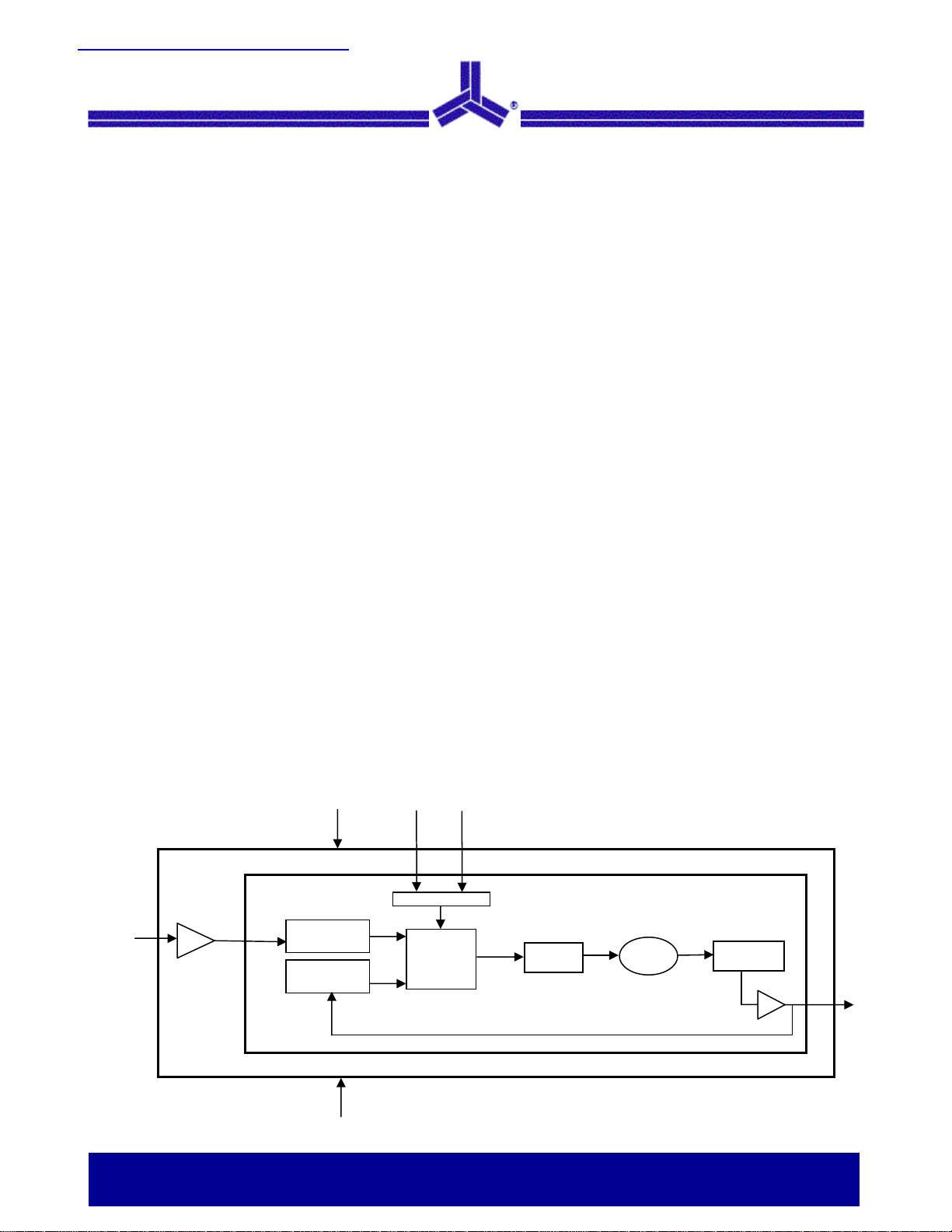
Functional Description
ASM3P623S00D/E/F is a versatile, 3.3V zero-delay buffer
designed to distribute high-speed clocks. It accepts one
reference input and drives out eight low-skew clocks. It is
available in a 16pin package. The ASM3P623S00A/B/C is
the eight-pin version of the ASM3P623S00. It accepts one
reference input and drives out one low-skew clock.
Block Diagram
VDD
SSON
All parts have on-chip PLLs that lock to an input clock on
the CLKIN pin. The PLL feedback is on-chip and is
obtained from the CLKOUT pad, internal to the device.
Multiple ASM3P623S00D/E/F devices can accept the same
input clock and distribute it. In this case, the skew between
the outputs of the two devices is guaranteed to be less than
700pS.
All outputs have less than 200pS of cycle-to-cycle jitter.
The input and output propagation delay is guaranteed to be
less than 250pS, and the output-to-output skew is
guaranteed to be less than 250pS.
Please refer
“Differential Cycle Slips and Spread Spectrum
Control Table” for deviations and differential Cycle Slips
for ASM3P623S00A/B/C and the ASM3P623S00D/E/F
devices
The ASM3P623S00A/B/C and the ASM3P623S00D/E/F
are available in two different configurations, as shown in
the ordering information table.
SS%
CLKIN
Reference
Divide
Feedback
Divide
Modulation
Phase
Detecto
Loop
Filte
VCO
PLL
Feedforward
Divide
CLKOUT
VSS
Alliance Semiconductor
2575 Augustine Drive • Santa Clara, CA • Tel: 408.855.4900 • Fax: 408.855.4999 • www.alsc.com
Notice: The information in this document is subject to change without notice.
Page 2
July 2005
ASM3P623S00A/B/C/D/E/F
rev 1.0
Spread Spectrum Frequency Generation
The clocks in digital systems are typically square waves
with a 50% duty cycle and as frequencies increase the
edge rates also get faster. Analysis shows that a square
wave is composed of fundamental frequency and
harmonics. The fundamental frequency and harmonics
generate the energy peaks that become the source of
EMI. Regulatory agencies test electronic equipment by
measuring the amount of peak energy radiated from the
equipment. In fact, the peak level allowed decreases as
the frequency increases. The standard methods of
reducing EMI are to use shielding, filtering, multi-layer
Cycle Slip
Cycle slip occurs when the output clock edge
‘wanders’ away from the corresponding input clock
edge. There are two types of cycle slips – a Differential
cycle slip and an Integral cycle slip. The differential
cycle slip is caused due the clock edge variation over
one modulation cycle. It is defined by the maximum
amount of ‘wander’ the clock edge will have within one
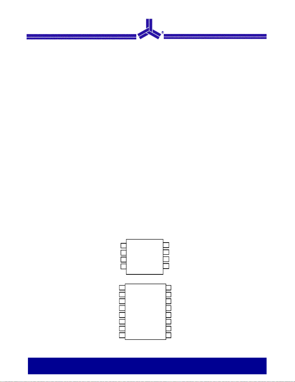
Pin Configuration
PCBs etc. These methods are expensive. Spread
spectrum clocking reduces the peak energy by reducing
the Q factor of the clock. This is done by slowly
modulating the clock frequency. The ASM3P623S00X
uses the center modulation spread spectrum technique in
which the modulated output frequency varies above and
below the reference frequency with a specified
modulation rate. With center modulation, the average
frequency is the same as the unmodulated frequency and
there is no performance degradation
modulation cycle. Integral cycle slip occurs due to the
accumulation of the cycle slip over successive modulation
cycles. In ASM3P623S00A/B/C/D/E/F the differential cycle
slip is within the value mentioned in the
“Differential Cycle
Slip and Spread Spectrum Control Table” and the Integral
Cycle Slip is ‘Zero’.
NC
CLKIN
NC
SS%
GND
1
2
ASM3P623S00A/B/C
3
4
8
7
6
5
V
DD
CLKOUT
SSON
1
CLKIN
VDD
SS%
GND
2
3
4
ASM3P623S00 D/E/F
5
6
7
8
CLKOUT1
CLKOUT2
CLKOUT3
DLY CNTRL
16
15
14
13
12
11
10
9
CLKOUT8
CLKOUT7
CLKOUT6
VDD
GND
CLKOUT5
CLKOUT4
SSON
Zero Cycle Slip Peak EMI Reduction IC 2 of 16
Notice: The information in this document is subject to change without notice.
Page 3

July 2005
ASM3P623S00A/B/C/D/E/F
rev 1.0
Pin Description for ASM3P623S00A/B/C
Pin # Pin Name Description
1 CLKIN2 Input reference frequency, 5V-tolerant input
2 NC No Connect
3 SS%4 Spread Spectrum Selection
4 GND Ground
5 SSON4 Spread Spectrum enable and disable option When SSON is HIGH, the spread
spectrum is enabled and when LOW, it turns off the spread spectrum.
6 CLKOUT
7 VDD 3.3V supply
8 NC No Connect
Pin Description for ASM3P623S00D/E/F
Pin # Pin Name Description
1 CLKIN2 Input reference frequency, 5V tolerant input
2 CLKOUT13 Buffered clock output
3 VDD 3.3V supply
4 SS%4 Spread Spectrum Selection
5 GND Ground
6 CLKOUT23 Buffered clock output
7 CLKOUT33 Buffered clock output
8 DLY CNTRL
9 SSON4
10 CLKOUT43 Buffered clock output
11 CLKOUT53 Buffered clock output
12 GND Ground
13 VDD 3.3V supply
14 CLKOUT63 Buffered clock output
15 CLKOUT73 Buffered clock output
16 CLKOUT83 Buffered clock output
Notes:
1. This output is driven and has an internal feedback for the PLL.
2. Weak pull-down. 3. Weak pull-down on all outputs. 4. Weak pull-up on these inputs.
1,3
Buffered clock output
The pin is used to skew the outputs such that they align with the input. The skew can
is in the range of 100-200pS
Spread Spectrum enable and disable option. When SSON is HIGH, the spread
spectrum is enabled and when LOW, it turns off the spread spectrum.
Zero Cycle Slip Peak EMI Reduction IC 3 of 16
Notice: The information in this document is subject to change without notice.
Page 4
July 2005
ASM3P623S00A/B/C/D/E/F
rev 1.0
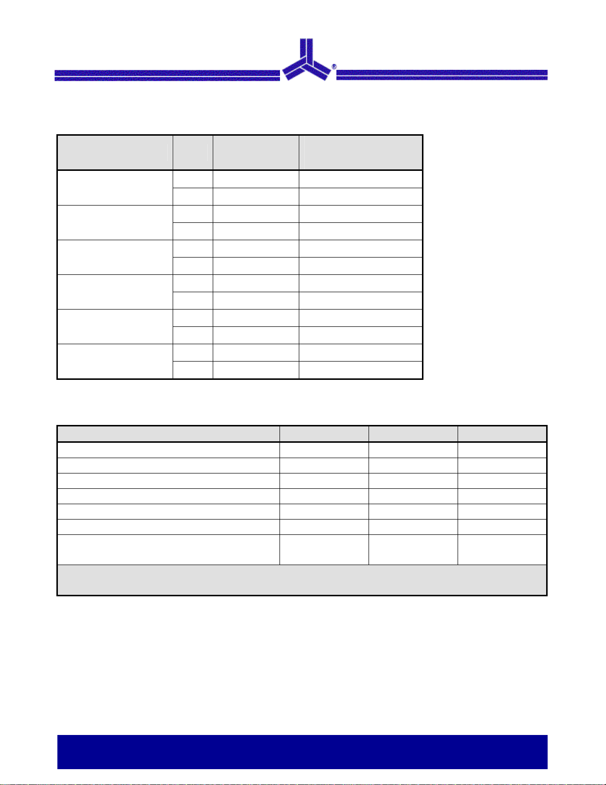
Differential Cycle Slips and Spread Spectrum Control Table
(Note: The values given in the table are for an input frequency of 32 MHz)
Device SS% Deviation
ASM3P623S00A
ASM3P623S00B
ASM3P623S00C
ASM3P623S00D
ASM3P623S00E
0 ±0.5 % 0.125
1 ±1 % 0.25
0 ±0.25 % 0.125
1 ±0.5 % 0.25
0 ±0.125 % 0.125
1 ±0.25 % 0.25
0 ±0.5 % 0.125
1 ±1 % 0.25
0 ±0.25 % 0.125
1 ±0.5 % 0.25
Differential Cycle Slips
(Nd)
ASM3P623S00F
0 ±0.125 % 0.125
1 ±0.25 % 0.25
Absolute Maximum Ratings
Parameter Min Max Unit
Supply Voltage to Ground Potential -0.5 +7.0 V
DC Input Voltage (Except CLKIN) -0.5 VDD + 0.5 V
DC Input Voltage (CLKIN) -0.5 7 V
Storage Temperature -65 +150 °C
Max. Soldering Temperature (10 sec) 260 °C
Junction Temperature 150 °C
Static Discharge Voltage
(As per JEDEC STD22- A114-B)
Note: These are stress ratings only and functional usage is not implied. Exposure to absolute maximum ratings for prolonged periods can affect device
reliability.
2000 V
Zero Cycle Slip Peak EMI Reduction IC 4 of 16
Notice: The information in this document is subject to change without notice.
Page 5

July 2005
ASM3P623S00A/B/C/D/E/F
rev 1.0
Operating Conditions for ASM3P623S00A/B/C and ASM3P623S00D/E/F Devices
Parameter Description Min Max Unit
VDD Supply Voltage 3.0 3.6 V
TA Operating Temperature (Ambient Temperature) 0 70 °C
CL Load Capacitance 30 pF
CIN Input Capacitance 7 pF
Electrical Characteristics for ASM3P623S00A/B/C and ASM3P623S00D/E/F
Parameter Description Test Conditions Min Typ Max Unit
VIL Input LOW Voltage5 0.8 V
VIH Input HIGH Voltage5 2.0 V
IIL Input LOW Current VIN = 0V 50 µA
IIH Input HIGH Current VIN = VDD 100 µA
VOL Output LOW Voltage6 I
VOH Output HIGH Voltage6 I
IDD Supply Current Unloaded outputs 15 mA
Zo Output Impedance 23 Ω
Switching Characteristics for ASM3P623S00A/B/C and ASM3P623S00D/E/F
= 8mA 0.4 V
OL
= -8mA 2.4 V
OH
7
Parameter Description Test Conditions Min Typ Max Unit
1/t1 Output Frequency 30pF load 20 50 MHz
Duty Cycle
t3 Output Rise Time 6 Measured between 0.8V and 2.0V 2.5 nS
t4 Output Fall Time 6 Measured between 2.0V and 0.8V 2.5 nS
t5 Output-to-output skew
t6 Delay, CLKIN Rising Edge to
CLKOUT Rising Edge
t7 Device-to-Device Skew
tJ Cycle-to-cycle jitter
t
PLL Lock Time 6 Stable power supply, valid clock presented
LOCK
Notes:
5. CLKIN input has a threshold voltage of VDD/2
6. Parameter is guaranteed by design and characterization. Not 100% tested in production
7. All parameters specified with loaded outputs.
6
= (t2 / t1) * 100 Measured at VDD/2 40 50 60 %
6
All outputs equally loaded 250 pS
Measured at VDD /2
6
6
Measured at VDD/2 on the CLKOUT pins
of the device
6
Loaded outputs 200 pS
on CLKIN pin
±350 pS
700 pS
1.0 mS
Zero Cycle Slip Peak EMI Reduction IC 5 of 16
Notice: The information in this document is subject to change without notice.
Page 6

V
July 2005
ASM3P623S00A/B/C/D/E/F
rev 1.0
Switching Waveforms
Duty Cycle Timing
t
2
1. 4 V
All Outputs Rise/Fall Time
2.0 V
OUTPUT
0. 8 V
t3
Output - Output Skew
1.4 V 1.4 V
t
1
2. 0 V
0.8 V
t4
3. 3
0 V
OUTPUT
OUTPUT
1. 4 V
1.4 V
t
5
Input - Output Propagation Delay
VDD/2
INPUT
OUTPUT
VDD/2
t
6
Device - Device Skew
CLKOUT , Device 1
CLKOUT , Device 2
VDD/2
VDD/2
t
7
Zero Cycle Slip Peak EMI Reduction IC 6 of 16
Notice: The information in this document is subject to change without notice.
Page 7

p
July 2005
ASM3P623S00A/B/C/D/E/F
rev 1.0
Differential cycle slip
Test Circuits
-Nd
+Nd
Nd represents the differential cycle slip
when spread spectrum is ON
Nd = ± 0.125 in the exam
TEST CIRCUIT # 1
Input
One clock cycle
N=1
VDD
Modulated
Output
le
0.1uF
0.1uF
OUTPUTS
VDD
GND GND
CLOAD
Zero Cycle Slip Peak EMI Reduction IC 7 of 16
Notice: The information in this document is subject to change without notice.
Page 8

C
July 2005
ASM3P623S00A/B/C/D/E/F
rev 1.0
Package Information
D
e
B
Symbol
8-lead (150-mil) SOIC Package
H
E
A2
A
A1
D
θ
L
Dimensions
Inches
Millimeters
Min Max Min Max
A1 0.004 0.010 0.10 0.25
A 0.053 0.069 1.35 1.75
A2 0.049 0.059 1.25 1.50
B 0.012 0.020 0.31 0.51
C 0.007 0.010 0.18 0.25
D 0.193 BSC 4.90 BSC
E 0.154 BSC 3.91 BSC
e 0.050 BSC 1.27 BSC
H 0.236 BSC 6.00 BSC
L 0.016 0.050 0.41 1.27
θ 0° 8° 0° 8°
Zero Cycle Slip Peak EMI Reduction IC 8 of 16
Notice: The information in this document is subject to change without notice.
Page 9

C
July 2005
rev 1.0
ASM3P623S00A/B/C/D/E/F
8-lead Thin Shrunk Small Outline Package (4.40-MM Body)
H
E
D
e
B
A2
A
θ
A1
L
Dimensions
Symbol
Inches Millimeters
Min Max Min Max
A
A1 0.002 0.006 0.05 0.15
A2 0.033 0.037 0.85 0.95
B 0.008 0.012 0.19 0.30
c 0.004 0.008 0.09 0.20
D 0.114 0.122 2.90 3.10
E 0.169 0.177 4.30 4.50
e 0.026 BSC 0.65 BSC
H 0.252 BSC 6.40 BSC
L 0.020 0.028 0.50 0.70
θ 0° 8° 0° 8°
0.043
1.10
Zero Cycle Slip Peak EMI Reduction IC 9 of 16
Notice: The information in this document is subject to change without notice.
Page 10

C
July 2005
rev 1.0
ASM3P623S00A/B/C/D/E/F
16-lead (150 Mil) Molded SOIC Package
E
A1
PI N 1 ID
H
A
D
0.004
Seating Plane
h
θ
L
8
916
D
e
1
A2
B
Symbol
Inches Millimeters
Dimensions
Min Max Min Max
A 0.053 0.069 1.35 1.75
A1 0.004 0.010 0.10 0.25
A2 0.049 0.059 1.25 1.50
B 0.013 0.022 0.33 0.53
C 0.008 0.012 0.19 0.27
D 0.386 0.394 9.80 10.01
E 0.150 0.157 3.80 4.00
e 0.050 BSC 1.27 BSC
H 0.228 0.244 5.80 6.20
h 0.010 0.016 0.25 0.41
L 0.016 0.035 0.40 0.89
θ 0° 8° 0° 8°
Zero Cycle Slip Peak EMI Reduction IC 10 of 16
Notice: The information in this document is subject to change without notice.
Page 11

C
July 2005
rev 1.0
ASM3P623S00A/B/C/D/E/F
16-lead Thin Shrunk Small Outline Package (4.40-MM Body)
8
9
e
D
1
PIN 1 ID
E
H
16
B
A2
A1
A
Seating Plane
D
θ
L
Symbol
Inches Millimeters
Dimensions
Min Max Min Max
A 0.043 1.20
A1 0.002 0.006 0.05 0.15
A2 0.031 0.041 0.80 1.05
B 0.007 0.012 0.19 0.30
C 0.004 0.008 0.09 0.20
D 0.193 0.201 4.90 5.10
E 0.169 0.177 4.30 4.50
e 0.026 BSC 0.65 BSC
H 0.252 BSC 6.40 BSC
L 0.020 0.030 0.50 0.75
θ 0° 8° 0° 8°
Zero Cycle Slip Peak EMI Reduction IC 11 of 16
Notice: The information in this document is subject to change without notice.
Page 12

July 2005
ASM3P623S00A/B/C/D/E/F
rev 1.0
Ordering Codes
Ordering Code Marking Package Type Operating Range
ASM3P623S00DF-16-ST 3P623S00DF 16-pin 150-mil SOIC-TUBE, Pb Free Commercial
ASM3P623S00EF-16-ST 3P623S00EF 16-pin 150-mil SOIC- TUBE, Pb Free Commercial
ASM3P623S00FF-16-ST 3P623S00FF 16-pin 150-mil SOIC- TUBE, Pb Free Commercial
ASM3I623S00DF-16-ST 3I623S00DF 16-pin 150-mil SOIC-TUBE, Pb Free Industrial
ASM3I623S00EF-16-ST 3I623S00EF 16-pin 150-mil SOIC- TUBE, Pb Free
ASM3I623S00FF-16-ST 3I623S00FF 16-pin 150-mil SOIC- TUBE, Pb Free
ASM3P623S00DF-16-SR 3P623S00DF 16-pin 150-mil SOIC-TAPE & REEL, Pb Free Commercial
ASM3P623S00EF-16-SR 3P623S00EF 16-pin 150-mil SOIC-TAPE & REEL, Pb Free Commercial
ASM3P623S00FF-16-SR 3P623S00FF 16-pin 150-mil SOIC-TAPE & REEL, Pb Free Commercial
ASM3I623S00DF-16-SR 3I623S00DF 16-pin 150-mil SOIC-TAPE & REEL, Pb Free Industrial
ASM3I623S00EF-16-SR 3I623S00EF 16-pin 150-mil SOIC-TAPE & REEL, Pb Free
ASM3I623S00FF-16-SR 3I623S00FF 16-pin 150-mil SOIC-TAPE & REEL, Pb Free
ASM3P623S00DF-16-TT 3P623S00DF 16-pin 4.4-mm TSSOP - TUBE, Pb Free Commercial
ASM3P623S00EF-16-TT 3P623S00EF 16-pin 4.4-mm TSSOP - TUBE, Pb Free Commercial
ASM3P623S00FF-16-TT 3P623S00FF 16-pin 4.4-mm TSSOP - TUBE, Pb Free Commercial
ASM3I623S00DF-16-TT 3I623S00DF 16-pin 4.4-mm TSSOP - TUBE, Pb Free Industrial
ASM3I623S00EF-16-TT 3I623S00EF 16-pin 4.4-mm TSSOP - TUBE, Pb Free
ASM3I623S00FF-16-TT 3I623S00FF 16-pin 4.4-mm TSSOP - TUBE, Pb Free
ASM3P623S00DF-16-TR 3P623S00DF 16-pin 4.4-mm TSSOP - TAPE & REEL, Pb Free Commercial
ASM3P623S00EF-16-TR 3P623S00EF 16- pin 4.4-mm TSSOP - TAPE & REEL, Pb Free Commercial
ASM3P623S00FF-16-TR 3P623S00FF 16- pin 4.4-mm TSSOP - TAPE & REEL, Pb Free Commercial
ASM3I623S00DF-16-TR 3I623S00DF 16-pin 4.4-mm TSSOP - TAPE & REEL, Pb Free Industrial
ASM3I623S00EF-16-TR 3I623S00EF 16- pin 4.4-mm TSSOP - TAPE & REEL, Pb Free
ASM3I623S00FF-16-TR 3I623S00FF 16- pin 4.4-mm TSSOP - TAPE & REEL, Pb Free
ASM3P623S00AF-08-ST 3P623S00AF 8-pin 150-mil SOIC-TUBE, Pb Free Commercial
ASM3P623S00BF-08-ST 3P623S00BF 8-pin 150-mil SOIC- TUBE, Pb Free Commercial
ASM3P623S00CF-08-ST 3P623S00CF 8-pin 150-mil SOIC- TUBE, Pb Free Commercial
ASM3I623S00AF-08-ST 3I623S00AF 8-pin 150-mil SOIC-TUBE, Pb Free Industrial
ASM3I623S00BF-08-ST 3I623S00BF 8-pin 150-mil SOIC- TUBE, Pb Free
ASM3I623S00CF-08-ST 3I623S00CF 8-pin 150-mil SOIC- TUBE, Pb Free
ASM3P623S00AF-08-SR 3P623S00AF 8-pin 150-mil SOIC-TAPE & REEL, Pb Free Commercial
ASM3P623S00BF-08-SR 3P623S00BF 8-pin 150-mil SOIC-TAPE & REEL, Pb Free Commercial
Industrial
Industrial
Industrial
Industrial
Industrial
Industrial
Industrial
Industrial
Industrial
Industrial
Zero Cycle Slip Peak EMI Reduction IC 12 of 16
Notice: The information in this document is subject to change without notice.
Page 13

July 2005
ASM3P623S00A/B/C/D/E/F
rev 1.0
Ordering Codes (cont’d)
Ordering Code Marking Package Type Operating
Range
ASM3P623S00CF-08-SR 3P623S00CF 8-pin 150-mil SOIC-TAPE & REEL, Pb Free Commercial
ASM3I623S00AF-08-SR 3I623S00AF 8-pin 150-mil SOIC-TAPE & REEL, Pb Free Industrial
ASM3I623S00BF-08-SR 3I623S00BF 8-pin 150-mil SOIC-TAPE & REEL, Pb Free
ASM3I623S00CF-08-SR 3I623S00CF 8-pin 150-mil SOIC-TAPE & REEL, Pb Free
Industrial
Industrial
ASM3P623S00AF-08-TT 3P623S00AF 8-pin 4.4-mm TSSOP - TUBE, Pb Free Commercial
ASM3P623S00BF-08-TT 3P623S00BF 8-pin 4.4-mm TSSOP - TUBE, Pb Free Commercial
ASM3P623S00CF-08-TT 3P623S00CF 8-pin 4.4-mm TSSOP - TUBE, Pb Free Commercial
ASM3I623S00AF-08-TT 3I623S00AF 8-pin 4.4-mm TSSOP - TUBE, Pb Free Industrial
ASM3I623S00BF-08-TT 3I623S00BF 8-pin 4.4-mm TSSOP - TUBE, Pb Free
ASM3I623S00CF-08-TT 3I623S00BF 8-pin 4.4-mm TSSOP - TUBE, Pb Free
Industrial
Industrial
ASM3P623S00AF-08-TR 3P623S00AF 8-pin 4.4-mm TSSOP - TAPE & REEL, Pb Free Commercial
ASM3P623S00BF-08-TR 3P623S00BF 8- pin 4.4-mm TSSOP - TAPE & REEL, Pb Free Commercial
ASM3P623S00CF-08-TR 3P623S00CF 8-pin 4.4-mm TSSOP - TAPE & REEL, Pb Free Commercial
ASM3I623S00AF-08-TR 3I623S00AF 8-pin 4.4-mm TSSOP - TAPE & REEL, Pb Free Industrial
ASM3I623S00BF-08-TR 3I623S00BF 8-pin 4.4-mm TSSOP - TAPE & REEL, Pb Free
ASM3I623S00CF-08-TR 3I623S00CF 8-pin 4.4-mm TSSOP - TAPE & REEL, Pb Free
Industrial
Industrial
Zero Cycle Slip Peak EMI Reduction IC 13 of 16
Notice: The information in this document is subject to change without notice.
Page 14

July 2005
ASM3P623S00A/B/C/D/E/F
rev 1.0
Ordering Codes (cont’d)
Ordering Code Marking Package Type Operating Range
ASM3P623S00DG-16-ST 3P623S00DG 16-pin 150-mil SOIC-TUBE, Green Commercial
ASM3P623S00EG-16-ST 3P623S00EG 16-pin 150-mil SOIC- TUBE, Green Commercial
ASM3P623S00FG-16-ST 3P623S00FG 16-pin 150-mil SOIC- TUBE, Green Commercial
ASM3I623S00DG-16-ST 3I623S00DG 16-pin 150-mil SOIC-TUBE, Green Industrial
ASM3I623S00EG-16-ST 3I623S00EG 16-pin 150-mil SOIC- TUBE, Green
ASM3I623S00FG-16-ST 3I623S00FG 16-pin 150-mil SOIC- TUBE, Green
ASM3P623S00DG-16-SR 3P623S00DG 16-pin 150-mil SOIC-TAPE & REEL, Green Commercial
ASM3P623S00EG-16-SR 3P623S00EG 16-pin 150-mil SOIC-TAPE & REEL, Green Commercial
ASM3P623S00FG-16-SR 3P623S00FG 16-pin 150-mil SOIC-TAPE & REEL, Green Commercial
ASM3I623S00DG-16-SR 3I623S00DG 16-pin 150-mil SOIC-TAPE & REEL, Green Industrial
ASM3I623S00EG-16-SR 3I623S00EG 16-pin 150-mil SOIC-TAPE & REEL, Green
ASM3I623S00FG-16-SR 3I623S00FG 16-pin 150-mil SOIC-TAPE & REEL, Green
ASM3P623S00DG-16-TT 3P623S00DG 16-pin 4.4-mm TSSOP - TUBE, Green Commercial
ASM3P623S00EG-16-TT 3P623S00EG 16-pin 4.4-mm TSSOP - TUBE, Green Commercial
ASM3P623S00FG-16-TT 3P623S00FG 16-pin 4.4-mm TSSOP - TUBE, Green Commercial
ASM3I623S00DG-16-TT 3I623S00DG 16-pin 4.4-mm TSSOP - TUBE, Green Industrial
ASM3I623S00EG-16-TT 3I623S00EG 16-pin 4.4-mm TSSOP - TUBE, Green
ASM3I623S00FG-16-TT 3I623S00FG 16-pin 4.4-mm TSSOP - TUBE, Green
ASM3P623S00DG-16-TR 3P623S00DG 16-pin 4.4-mm TSSOP - TAPE & REEL, Green Commercial
ASM3P623S00EG-16-TR 3P623S00EG 16- pin 4.4-mm TSSOP - TAPE & REEL, Green Commercial
ASM3P623S00FG-16-TR 3P623S00FG 16- pin 4.4-mm TSSOP - TAPE & REEL, Green Commercial
ASM3I623S00DG-16-TR 3I623S00DG 16-pin 4.4-mm TSSOP - TAPE & REEL, Green Industrial
ASM3I623S00EG-16-TR 3I623S00EG 16- pin 4.4-mm TSSOP - TAPE & REEL, Green
ASM3I623S00FG-16-TR 3I623S00FG 16- pin 4.4-mm TSSOP - TAPE & REEL, Green
ASM3P623S00AG-08-ST 3P623S00AG 8-pin 150-mil SOIC-TUBE, Green Commercial
ASM3P623S00BG-08-ST 3P623S00BG 8-pin 150-mil SOIC- TUBE, Green Commercial
ASM3P623S00CG-08-ST 3P623S00CG 8-pin 150-mil SOIC- TUBE, Green Commercial
ASM3I623S00AG-08-ST 3I623S00AG 8-pin 150-mil SOIC-TUBE, Green Industrial
ASM3I623S00BG-08-ST 3I623S00BG 8-pin 150-mil SOIC- TUBE, Green
ASM3I623S00CG-08-ST 3I623S00CG 8-pin 150-mil SOIC- TUBE, Green
ASM3P623S00AG-08-SR 3P623S00AG 8-pin 150-mil SOIC-TAPE & REEL, Green Commercial
ASM3P623S00BG-08-SR 3P623S00BG 8-pin 150-mil SOIC-TAPE & REEL, Green Commercial
ASM3P623S00CG-08-SR 3P623S00CG 8-pin 150-mil SOIC-TAPE & REEL, Green Commercial
ASM3I623S00AG-08-SR 3I623S00AG 8-pin 150-mil SOIC-TAPE & REEL, Green Industrial
Industrial
Industrial
Industrial
Industrial
Industrial
Industrial
Industrial
Industrial
Industrial
Industrial
Zero Cycle Slip Peak EMI Reduction IC 14 of 16
Notice: The information in this document is subject to change without notice.
Page 15

y
July 2005
ASM3P623S00A/B/C/D/E/F
rev 1.0
Ordering Codes (cont’d)
Ordering Code Marking Package Type Operating Range
ASM3I623S00BG-08-SR 3I623S00BG 8-pin 150-mil SOIC-TAPE & REEL, Green
ASM3I623S00CG-08-SR 3I623S00CG 8-pin 150-mil SOIC-TAPE & REEL, Green
ASM3P623S00AG-08-TT 3P623S00AG 8-pin 4.4-mm TSSOP - TUBE, Green Commercial
ASM3P623S00BG-08-TT 3P623S00BG 8-pin 4.4-mm TSSOP - TUBE, Green Commercial
ASM3P623S00CG-08-TT 3P623S00CG 8-pin 4.4-mm TSSOP - TUBE, Green Commercial
ASM3I623S00AG-08-TT 3I623S00AG 8-pin 4.4-mm TSSOP - TUBE, Green Industrial
ASM3I623S00BG-08-TT 3I623S00BG 8-pin 4.4-mm TSSOP - TUBE, Green
ASM3I623S00CG-08-TT 3I623S00BG 8-pin 4.4-mm TSSOP - TUBE, Green
ASM3P623S00AG-08-TR 3P623S00AG 8-pin 4.4-mm TSSOP - TAPE & REEL, Green Commercial
ASM3P623S00BG-08-TR 3P623S00BG 8- pin 4.4-mm TSSOP - TAPE & REEL, Green Commercial
ASM3P623S00CG-08-TR 3P623S00CG 8-pin 4.4-mm TSSOP - TAPE & REEL, Green Commercial
ASM3I623S00AG-08-TR 3I623S00AG 8-pin 4.4-mm TSSOP - TAPE & REEL, Green Industrial
ASM3I623S00BG-08-TR 3I623S00BG 8-pin 4.4-mm TSSOP - TAPE & REEL, Green
ASM3I623S00CG-08-TR 3I623S00CG 8-pin 4.4-mm TSSOP - TAPE & REEL, Green
Industrial
Industrial
Industrial
Industrial
Industrial
Industrial
Device Ordering Information
ASM3P623S00AF-08-TR
Licensed under US patent #5,488,627, #6,646,463 and #5,631,920.
R = Tape & reel, T = Tube or Tray
O = SOT U = MSOP
S = SOIC E = TQFP
T = TSSOP L = LQFP
A = SSOP U = MSOP
V = TVSOP P = PDIP
B = BGA D = QSOP
=
DEVICE PIN COUNT
F = LEAD FREE AND RoHS COMPLIANT PART
G = GREEN PACKAGE
PART NUMBER
X= Automotive I= Industrial P or n/c = Commercial
(-40C to +125C) (-40C to +85C) (0C to +70C)
1 = Reserved 6 = Power Management
2 = Non PLL based 7 = Power Management
3 = EMI Reduction 8 = Power Management
4 = DDR support products 9 = Hi Performance
5 = STD Zero Dela
ALLIANCE SEMICONDUCTOR MIXED SIGNAL PRODUCT
Buffer 0 = Reserved
=
-
Zero Cycle Slip Peak EMI Reduction IC 15 of 16
Notice: The information in this document is subject to change without notice.
Page 16

July 2005
ASM3P623S00A/B/C/D/E/F
rev 1.0
Alliance Semiconductor Corporation
2575 Augustine Drive,
Santa Clara, CA 95054
Tel# 408-855-4900
Fax: 408-855-4999
www.alsc.com
Note: This product utilizes US Patent # 6,646,463 Impedance Emulator Patent issued to Alliance Semiconductor, dated 11-11-2003
© Copyright 2003 Alliance Semiconductor Corporation. All rights reserved. Our three-point logo, our name and Intelliwatt are
trademarks or registered trademarks of Alliance. All other brand and product names may be the trademarks of their
respective companies. Alliance reserves the right to make changes to this document and its products at any time without
notice. Alliance assumes no responsibility for any errors that may appear in this document. The data contained herein
represents Alliance's best data and/or estimates at the time of issuance. Alliance reserves the right to change or correct this
data at any time, without notice. If the product described herein is under development, significant changes to these
specifications are possible. The information in this product data sheet is intended to be general descriptive information for
potential customers and users, and is not intended to operate as, or provide, any guarantee or warrantee to any user or
customer. Alliance does not assume any responsibility or liability arising out of the application or use of any product
described herein, and disclaims any express or implied warranties related to the sale and/or use of Alliance products
including liability or warranties related to fitness for a particular purpose, merchantability, or infringement of any intellectual
property rights, except as express agreed to in Alliance's Terms and Conditions of Sale (which are available from Alliance).
All sales of Alliance products are made exclusively according to Alliance's Terms and Conditions of Sale. The purchase of
products from Alliance does not convey a license under any patent rights, copyrights; mask works rights, trademarks, or any
other intellectual property rights of Alliance or third parties. Alliance does not authorize its products for use as critical
components in life-supporting systems where a malfunction or failure may reasonably be expected to result in significant
injury to the user, and the inclusion of Alliance products in such life-supporting systems implies that the manufacturer
assumes all risk of such use and agrees to indemnify Alliance against all claims arising from such use.
Copyright © Alliance Semiconductor
All Rights Reserved
Part Number: ASM3P623S00A/B/C/D/E/F
Document Version: 1.0
Zero Cycle Slip Peak EMI Reduction IC 16 of 16
Notice: The information in this document is subject to change without notice.
 Loading...