

Page 1
查询ASM1810供应商
February 2005
rev 1.4
Low Power, 5V µP Reset
- Active LOW, Push-Pull Output
General Description
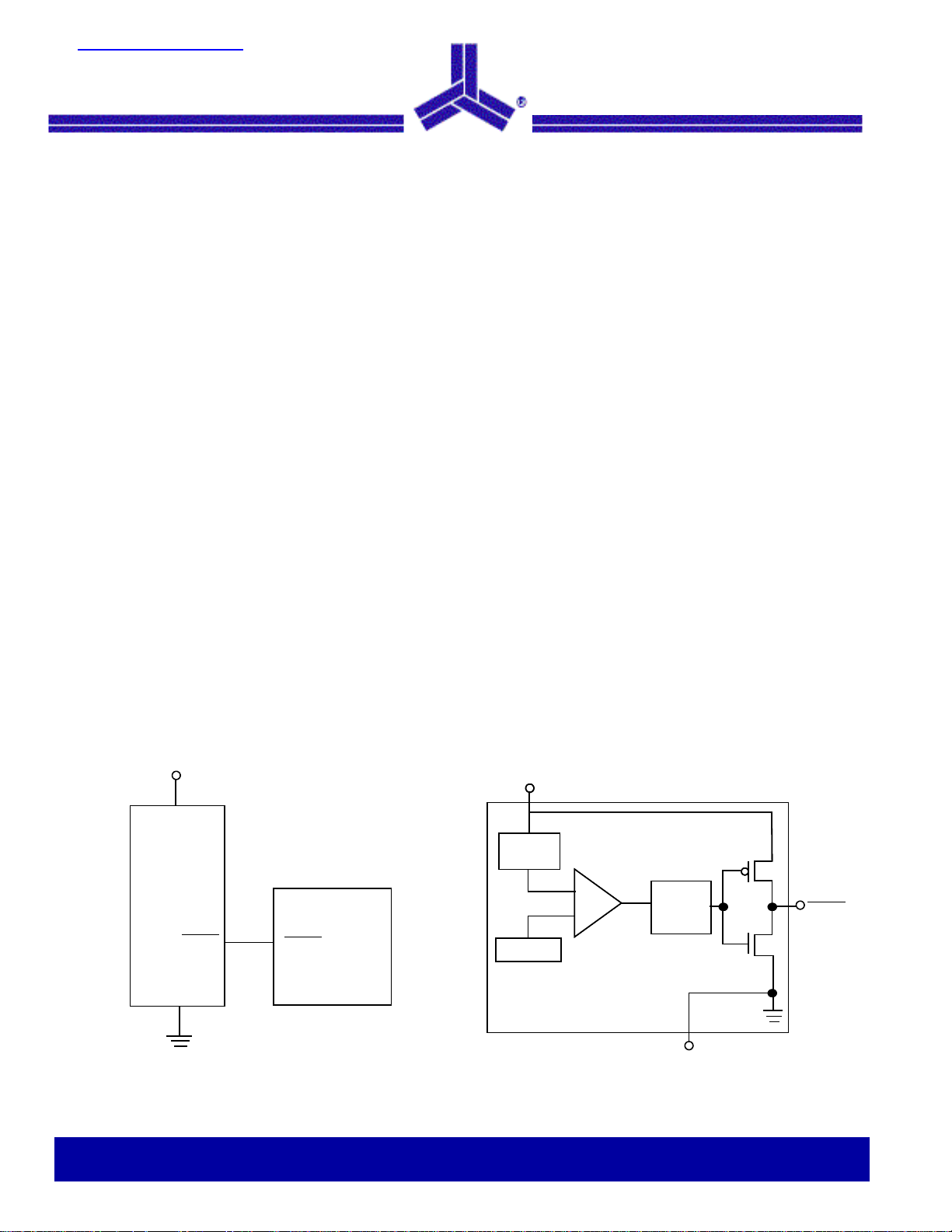
The ASM1810 is a voltage supervisor with low-power, 5V µP
active LOW Reset, Push-Pull output. Maximum supply current
over temperature is a low 20µA.
The ASM1810 generates an active LOW reset signal whenever
the monitored supply is out of tolerance. A precision reference
and comparator circuit monitor power supply (V
Tolerance level options are 5%, 10% and 15%. When an out-of-
tolerance condition is detected, an internal power-fail signal is
generated which forces an active LOW reset signal. After V
returns to an in-tolerance condition, the reset signal remains
active for 150ms to allow the power supply and system
microprocessor to stabilize.
) level.
CC
ASM1810
Key Features
• Low Supply Current
•20 µA maximum (5.5 V)
• Automatically restarts a microprocessor after power failure
• 150ms reset delay after V
dition
• Active LOW power-up reset
• Precision temperature-compensated voltage reference and
comparator
• Eliminates external components
• Low cost TO-92 and compact surface mount SOT-23 pack-
CC
age
• Push-Pull output for minimum current drain
• Operating temperature -40°C to +85°C
returns to an in-tolerance con-
CC
The ASM1810 is designed with a push-pull output stage and
operates over the extended industrial temperature range.
Devices are available in low cost TO-92 and compact surface
mount SOT-23 packages.
Other low power products in this family include the ASM1811/
12/15/16/17, ASM1233D and ASM1233M.
Typical Operating Circuit
V
CC
ASM1810
Microprocessor
RESET
GND
RESET
Applications
• Set-top boxes
• Cellular phones
•PDAs
• Energy management systems
• Embedded control systems
• Printers
• Single board computers
Block Diagram
V
V
2
CC
CC
ASM1810
Supply
Supply
Tolerance
Tolerance
Bias
Bias
Reference
Reference
+
+
-
-
ASM1810
Delay
Delay
150ms
150ms
Typical
Typical
1
RESET
RESET
3
GND
Alliance Semiconductor
2575 Augustine Drive . Santa Clara, CA 95054 . Tel: 408.855.4900 . Fax: 408.855.4999 . www.alsc.com
Notice: The information in this document is subject to change without notice
Page 2
February 2005
rev 1.4
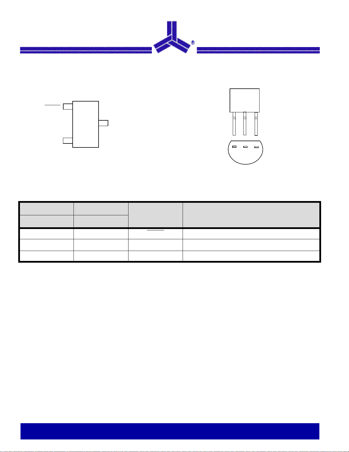
Pin Configuration
RESET
1
ASM1810
TO-92
SOT-23
ASM1810
V
CC
Pin Description
SOT-23 TO-92
Pin # Pin #
11RESET
22
3 3 GND Ground
ASM1810-R
2
GND
3
2
1
Pin Name Description
Active LOW reset output
V
CC
Power supply input
3
Low Power, 5V µP Reset
Notice: The information in this document is subject to change without notice
2 of 9
Page 3
February 2005
rev 1.4
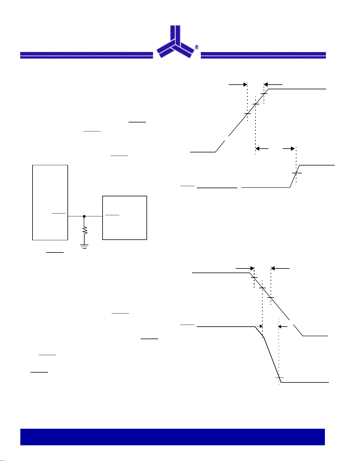
Application Information
ASM1810
Operation - Power Monitor
The ASM1810 detects out-of-tolerance power supply
conditions. It resets a processor during power-up, power-down
and issues a reset to the system processor when the monitored
power supply voltage is below the reset threshold. When an
out-of-tolerance V
asserted. On power-up, RESET is kept active (LOW) for
approximately 150ms after the power supply voltage has
reached the selected tolerance. This allows the power supply
and microprocessor to stabilize before RESET
voltage is detected, the RESET signal is
CC
is released.
ASM1810
Microprocessor
RESET
RESET
100kΩ
t
R
V
(MIN)
V
CCTP
~
~
V
CC
~
RESET
Figure 2: Timing Diagram: Power-Up
~
CCTP
V
t
RPU
CCTP
(MAX)
V
OH
Figure 1: RESET Valid to 0V V
Output Conditions
The ASM1810 active LOW reset signal is valid as long as V
remains above 1.2V. However the RESET output on the
ASM1810 uses a push-pull drive stage that can maintain a valid
output below 1.2V. To sink current with V
resistor can be connected from the reset pin (RESET) to
Ground (see Figure 1). This configuration will give a valid value
on the RESET
power up and down, this configuration will draw current when
the RESET is in the high state. A value of 100kΩ should be
adequate to maintain a valid connection.
output with VCC approaching 0V. During both
CC
below 1.2V, a
CC
CC
t
V
CCTP
F
t
RPD
V
OL
V
CC
V
(MAX)
CCTP
RESET
Figure 3: Timing Diagram: Power-Down
V
CCTP
(MIN)
~
~
Low Power, 5V µP Reset
Notice: The information in this document is subject to change without notice
3 of 9
Page 4

February 2005
rev 1.4
Absolute Maximum Ratings
ASM1810
Parameter Min Max Unit
Voltage on V
Voltage on RESET
Operating Temperature Range -40 85 °C
Soldering Temperature (for 10 sec) 260 °C
Storage Temperature -55 125 °C
CC
-0.5 7 V
V
-0.5
CC
+ 0.5
ESD rating
HBM
MM
NOTE: These are stress ratings only and functional use is not implied. Exposure to absolute maximum ratings for prolonged periods of time may affect device reliability.
2
200
Electrical Characteristics
Unless otherwise noted VCC = 1.25V to 5.5V and specifications are over the operating temperature range of -400c to +850c. All voltages are referenced to ground
Parameter Symbol Conditions Min Typ Max Unit
Supply voltage
Output voltage
Output Current
V
CC
V
OH
I
OH
I
< 500 µA VCC - 0.5V VCC - 0.1V
OUT
Output = 2.4V, VCC > 2.7V
1.2 5.5 V
350 µA
V
KV
V
V
Output Current
Operating Current
V
Trip Point (ASM1810R-5) V
CC
VCC Trip Point (ASM1810R-10) V
Trip Point (ASM1810R-15) V
V
CC
Output Capacitance
Detect to RESET Low t
V
CC
VCC Slew Rate
(V
(MAX) to V
CCTP
Slew Rate
V
CC
(V
(MIN) to V
CCTP
V
Detect to RESET High t
CC
Note: The tF value is for reference in defining values for t
CCTP
CCTP
(MIN)
(MAX)
I
OL
I
CC
CCTP
CCTP
CCTP
C
OUT
RPD
t
F
t
R
RPU
and should not be considered fo r proper operation or use.
RPD
Output = 0.4V, VCC > 2.7V
VCC < 5.5V, RESET output open
tr = 5µs
Low Power, 5V µP Reset
+10 mA
820µA
4.50 4.62 4.75 V
4.25 4.37 4.49 V
4.00 4.12 4.24 V
10 pF
25µs
300 µs
0ns
100 150 300 ms
4 of 9
Notice: The information in this document is subject to change without notice
Page 5

February 2005
rev 1.4
Family Selection Guide
ASM1810
Part # RESET Voltage (V)
ASM1810 4.620, 4.370, 4.120 150 Push-Pull LOW
ASM1811 4.620, 4.350, 4.130 150 Open-Drain LOW
ASM1812 4.620, 4.350, 4.130 150 Push-Pull HIGH
ASM1815 3.060, 2.880, 2.550 150 Push-Pull LOW
ASM1816 3.060, 2.880, 2.550 150 Open-Drain LOW
ASM1817 3.060, 2.880, 2.550 150 Push-Pull HIGH
ASM1233D 4.625, 4.375, 4.125 350 Open-Drain LOW
ASM1233M 4.625, 4.375, 2.720 350 Open-Drain LOW
RESET Time
(ms)
Output Stage RESET Polarity
Low Power, 5V µP Reset
Notice: The information in this document is subject to change without notice
5 of 9
Page 6

February 2005
rev 1.4
Package Dimension
Plastic SOT-23 (3-Pin)
D
B
ASM1810
E
H
S
A
A1
Inches Millimeters
Min Max Min Max
Plastic SOT-23 (3-Pin)
A 0.030 0.046 0.75 1.17
A1 0.002 0.006 0.05 0.15
B 0.012 0.020 0.30 0.50
e
e1
a
C
L
C 0.003 0.008 0.08 0.20
D 0.110 0.120 2.80 3.04
E 0.047 0.055 1.20 1.40
e 0.037 BSC 0.95 BSC
o
8
o
0
o
8
e1 0.075 BSC 1.9 BSC
H 0.083 0.104 2.10 2.64
L 0.016 0.024 0.40 0.60
a
SNA NA
o
0
Low Power, 5V µP Reset
Notice: The information in this document is subject to change without notice
6 of 9
Page 7

February 2005
rev 1.4
ASM1810
To-92 (3-Pin)
Dimensions in Inches Dimensions in Millimeters
Min Max Min Max
TO-92
A 0.175 0.185 4.445 4.699
b 0.016 0.020 0.406 0.508
C 0.014 0.016 0.356 0.406
φD 0.175 0.185 4.445 4.699
E 0.138 0.144 3.505 3.658
e 0.098 0.102 2.489 2.591
e1 0.045 0.055 1.143 1.397
j 0.168 0.174 4.269 4.420
L 0.500 0.585 12.7 14.86
s 0.095 0.099 2.413 2.515
Low Power, 5V µP Reset
Notice: The information in this document is subject to change without notice
7 of 9
Page 8

February 2005
rev 1.4
Ordering Information
ASM1810
Device Summary
RESET
Part ** Number
TIN - LEAD DEVICES
ASM1810R-5 4.62 5 150 LOW RALL
ASM1810R-10 4.37 10 150 LOW RBLL
ASM1810R-15 4.12 15 150 LOW RCLL
LEAD FREE DEVICES
ASM1810R-5F 4.62 5 150 LOW KALL
ASM1810R-10F 4.37 10 150 LOW KBLL
ASM1810R-15F 4.12 15 150 LOW KCLL
Part ** Number
TIN - LEAD DEVICES
ASM1810-5 4.62 5 150 LOW ASM1810-5
ASM1810-10 4.37 10 150 LOW ASM1810-10
Output
Voltage (V)
RESET
Output
Voltage (V)
RESET
Tolerance (%)
RESET
Tolerance (%)
RESET
Time (ms)
RESET
Time (ms)
Push-Pull
Output
Stage
Push-Pull
Output
Stage
SOT-23
Package
TO-92
Package
RESET
Polarity
RESET
Polarity
Package Marking
Package Marking
ASM1810-15 4.12 15 150 LOW ASM1810-15
LEAD FREE DEVICES
ASM1810-5F 4.62 5 150 LOW ASM1810-5F
ASM1810-10F 4.37 10 150 LOW ASM1810-10F
ASM1810-15F 4.12 15 150 LOW ASM1810-15F
** Add /T to Part Number for Tape and Reel (i.e ASM18xx-x/T)
LL - Lot Code
Low Power, 5V µP Reset
8 of 9
Notice: The information in this document is subject to change without notice
Page 9

ASM1810
Alliance Semiconductor Corporation
2575, Augustine Drive,
Santa Clara, CA 95054
Tel: 408 - 855 - 4900
Fax: 408 - 855 - 4999
www.alsc.com
© Copyright 2003 Alliance Semiconductor Corporation. All rights reserved. Our three-point logo, our name and Intelliwatt are trademarks or
registered trademarks of Alliance. All other brand and product names may be the trademarks of their respective companies. Alliance reserves the
right to make changes to this document and its products at any time without notice. Alliance assumes no responsibility for any errors that may
appear in this document. The data contained herein represents Alliance's best data and/or estimates at the time of issuance. Alliance reserves the
right to change or correct this data at any time, without notice. If the product described herein is under development, significant changes to these
specifications are possible. The information in this product data sheet is intended to be general descriptive information for potential customers and
users, and is not intended to operate as, or provide, any guarantee or warrantee to any user or customer. Alliance does not assume any responsibility
or liability arising out of the application or use of any product described herein, and disclaims any express or implied warranties related to the sale
and/or use of Alliance products including liability or warranties related to fitness for a particular purpose, merchantability, or infringement of any
intellectual property rights, except as express agreed to in Alliance's Terms and Conditions of Sale (which are available from Alliance). All sales of
Alliance products are made exclusively according to Alliance's Terms and Conditions of Sale. The purchase of products from Alliance does not
convey a license under any patent rights, copyrights; mask works rights, trademarks, or any other intellectual property rights of Alliance or third
parties. Alliance does not authorize its products for use as critical components in life-supporting systems where a malfunction or failure may
reasonably be expected to result in significant injury to the user, and the inclusion of Alliance products in such life-supporting systems implies that
the manufacturer assumes all risk of such use and agrees to indemnify Alliance against all claims arising from such use.
Copyright © Alliance Semiconductor
All Rights Reserved
Part Number: ASM1810
Document Version: 1.4
 Loading...