

Page 1
查询ASM162供应商
October 2003
rev 1.0
General Description
The ASM161 and ASM162 are cost effective, low power
supervisory circuits that monitor power supplies in
microprocessor, microcontroller and digital systems. If the
power supply drops below the reset threshold level, a reset is
asserted and remains asserted for atleast 800ms after V
risen above the reset threshold. An improved manual reset
architecture gives the system designer additional flexibility.
The debounced manual reset input is negative edge triggered.
The reset pulse period generated by a MR
minimum of 800 ms and a maximum of 2 sec duration. In
addition, The MR
minimum after the reset pulse ends. During the MR
period, the microcontroller is guaranteed a time period free of
additional manual reset signals. During this period DRAM
contents can be refreshed or other critical system tasks
undertaken. Low power consumption makes the ASM161/162
ideal for use in portable and battery operated equipments. With
3V supplies power consumption is 8µW typically and 30µW
maximum. The ASM161 has an open-drain, active-LOW
RESET
output and requires an external pull-up resistor. The
ASM162 has an active HIGH RESET output.
input signal is blocked for an additional 49µS
µP Supervisory Circuit
has
CC
transition is a
disable
ASM161 / ASM162
Key Features
• Edge triggered manual reset input
• single pulse output
• 49µS minimum MR
• CMOS/TTL logic or switch interface
• Debounced input
• Low supply current extends battery life
• 6µA / 15µA typ/max at 5.5V
• 4.5µA / 10µA typ/max at 3.6V
• Long reset period
• 0.8 sec minimum, 2 sec maximum
• Two reset polarity options
• ASM161: Active LOW, open-drain
• ASM162: Active HIGH
• Pinout matches the AS811/812
• Small 4-Pin SOT-143 package
• Two temperature ranges: 0
Applications
•PDAs
• Appliances
• Computers and embedded controllers
• Wireless communication systems
• Battery operated and intelligent instruments
• Automotive systems
• Safety systems
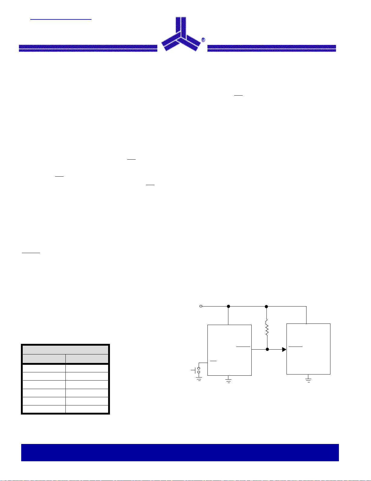
Typical Operating Circuit
disable period after reset
0
0
to 70
c and -400c to +850c
The ASM161/162 are offered in compact 4-pin SOT-143
packages. No external components are required to trim
threshold voltage for monitoring different supply voltages. With
six different factory set, reset, threshold ranges from 2.63V to
4.63V, the ASM161/162 are suitable for monitoring 5V, 3.6V
and 3.0V supplies. The ASM161/162 are available in
temperature ranges 0
Reset Threshold
Part Suffix Voltage (V)
L4.63
M4.38
J4.00
T3.08
S2.93
R2.63
0
to 700c and -400c to +850c.
Alliance Semiconductor
2575 Augustine Drive . Santa Clara, CA 95054 . Tel: 408.855.4900 . Fax: 408.855.4999 . www.alsc.com
Notice: The information in this document is subject to change without notice
V
CC
V
CC
ASM161
(ASM162)
MR
GND
RESET
(RESET)
20k for
ASM161
only
RESET
(RESET)
V
µP
GND
CC
Page 2
October 2003
rev 1.0
Block Diagram
4
V
CC
MR
Pin Configuration
Voltage
Divider
3
MR
Debounce
* Non-retriggerable, edge
triggered manual reset
ASM161 / ASM162
V
-
+
Bandgap
Reference
1
GND
SOT-143
ASM161/162
Circuit
Reset
* Edge Trigger
2
(ASM161)
RESET
RESET (ASM162)
ASM161
~
~
Reset
Circuit
~
~
SOT-143
CC
4
R
PU
2
GND
1
ASM161
RESET
2
RESET is open drain
Pin Description
Pin #
Pin Name Description
ASM161 ASM162
1 1 GND Ground.
2 - RESET
- 2 RESET
33MR
V
4
CC
GND
1
V
4
CC
ASM162
MR
3
Active-LOW, open-drain reset output. RESET remains LOW while VCC is below the
reset threshold and for 800ms minimum after V
An external pull-up resistor is needed.
Active HIGH reset output. RESET remains HIGH while V
threshold and for 800ms after V
Manual reset input. A negative going edge transition on MR asserts reset. Reset
remains asserted for one reset time-out period (800 ms min). This active-LOW
input has an internal pull-up resistor. It can be driven from a TTL or CMOS logic line
or shorted to ground with a switch. Leave open if unused.
RESET
2
rises above the reset threshold.
CC
CC
rises above the reset threshold.
CC
MR
3
is below the reset
44
V
Notice: The information in this document is subject to change without notice
CC
Power supply input voltage.
2 of 9
µP Supervisory Circuit
Page 3
October 2003
rev 1.0
ASM161 / ASM162
Detailed Descriptions
The reset function ensures the microprocessor is properly
reset and powers up into a known condition after a power
failure.
Reset Timing
A reset is generated whenever the supply voltage is below
the threshold level (V
800ms after VCC has risen above the reset threshold and is
guaranteed to be no more than 2 seconds. The rest signal
remains active as long as the monitored supply voltage is
below the internal threshold voltage.
The ASM161 has an open-drain, active LOW RESET
(which is guaranteed to be in the correct state for V
to 1.1 V). The ASM161 uses an external pull-up resistor.
Output leakage current is under 1µA. A high resistance value
can be used to minimize current drain.
The ASM162 generates an active-HIGH RESET output.
Part Number Reset Polarity
ASM161 LOW (use external pull-up resistor)
ASM162 HIGH
Manual Reset
The ASM161/162 have a unique manual reset circuit. A
negative going edge transition on MR
manual reset generates a single reset pulse of fixed length.
The output-reset pulse remains asserted for the Reset Active
Time-Out Period t
completed, the MR
but not more than 122µS. This period is specified as t
During the MR
guaranteed a time period free of new manual reset signals.
This period can be used to refresh critical DRAM contents or
other system tasks.
< VTH). The reset duration is at least
CC
output
down
CC
initiates the reset. A
and then clears. Once the reset pulse is
RP
input remains disabled for at least 49µS
disabled period, the microcontroller is
MRD
.
The MR
t
MRD
pulse.
The manual reset input has an internal 20kΩ pull-up resistor.
MR
pin must be taken HIGH and LOW again after the
period has been completed to initiate another reset
can be left open if not used.
t
MD
MR
RESET
*........
Triggering
Reset
Time-Out
MR input is blocked
Pulse
t
MRD
*Second and following edges ignored
Figure 1: Manual Reset Timing
Application Information
Glitch Resistance
The ASM161/162 are relatively immune to short duration
negative-going V
goes 100mV below the reset threshold and lasts 20s or less
will not typically cause a reset pulse.
Figure 2:
Valid Reset with V
To ensure that logic inputs connected to the ASM162 RESET
pin are in a known state when V
pull-down resistor at RESET is needed. The value is not
critical.
This scheme does not work with the open-drain outputs of
ASM161.
transients/glitches. A VCC transient that
CC
V
Power Supply
ASM162
MR
GND
CC
RESET
100K
Ω
RESET valid with VCC under 1.1V
CC under 1.1V
is under 1.1V, a 100kΩ
CC
Ready
for
next
MR
µP Supervisory Circuit
Notice: The information in this document is subject to change without notice
3 of 9
Page 4

October 2003
rev 1.0
Absolute Maximum Ratings
Parameter Min Max Unit
Pin Terminal Voltage with respect to Ground
ASM161 / ASM162
V
CC
RESET, RESET
Input Current at V
Rate of Rise at V
Power Dissipation (T
Operating Temperature Range -40 85 °C
Storage Temperature Range -65 160 °C
Lead Temperature (soldering, 10 sec) 300 °C
Note: These are stress ratings only and functional operation is not implied. Exposure to absolute maximum ratings for prolonged time periods may affect device reliability.
and MR -0.3
and MR
CC
CC
= 70°C)
A
-0.3 6.0 V
+ 0.3
V
CC
20 mA
100 V/µs
320 mW
V
µP Supervisory Circuit
Notice: The information in this document is subject to change without notice
4 of 9
Page 5

October 2003
ASM161 / ASM162
rev 1.0
Electrical Characteristics
Unless otherwise noted, VCC is over the full range and TA = 00 to 700c for ASM161/162 X C and TA = -400c to +850c for ASM161/
162 X E devices. Typical values at T
Parameter Symbol Conditions Min Typ Max Unit
Input Voltage (V
Range
Supply Current
(Unloaded)
Reset Threshold
CC
)
V
CC
I
CC
V
TH
= 250c, VCC = 5V for L/M/J devices, VCC = 3.3V for T/S devices and VCC = 3V for R devices
A
TA = 0°C to 70°C
TA = 0°C to 70°C,
= -40°C to +85°C
T
A
= 0°C to 70°C,
T
A
T
= -40°C to +85°C
A
L Devices
M devices
J devices
T devices
V
< 5.5V,
CC
L/M/J
< 3.6V,
V
CC
R/S/T
= 25°C
T
A
Note 1 4.50 4.75
= 25°C
T
A
Note 1 4.25 4.50
= 25°C
T
A
Note 1 3.89 4.10
T
= 25°C
A
Note 1 3.00 3.15
1.1 5.5 V
615
µA
4.5 10
4.56 4.63 4.70
4.31 4.38 4.45
3.93 4.00 4.06
V
3.04 3.08 3.11
= 25°C
S devices
R devices
Reset Threshold Temp
Coefficient
V
to reset delay VCC = VTH to (VTH -100mV)
CC
Reset Pulse Width
Minimum Pulse
MR
Width
MR
Glitch Immunity 100 ns
to RESET Propaga-
MR
tion Delay
T
t
CVTH
RPW
t
MR
t
MD
TA = 0°C to 70°C
TA = -40°C to 85°C
T
A
Note 1 2.85 3.00
= 25°C
T
A
Note 1 2.55 2.70
2.89 2.93 2.96
2.59 2.63 2.66
30
20 µS
800 1400 2000
560 2240
10 µS
0.5 µs
ppm/
°C
ms
µP Supervisory Circuit
Notice: The information in this document is subject to change without notice
5 of 9
Page 6

October 2003
rev 1.0
Parameter Symbol Conditions Min Typ Max Unit
ASM161 / ASM162
V
IH
V
IL
MR Input Threshold
Delay to MR Retrig-
MR
ger
MR pull-up resistance 10 20 30 KΩ
Low RESET
age (ASM161)
RESET
age Current (ASM161)
Low RESET
age (ASM162)
HIGH RESET Output
Voltage (ASM162)
output volt-
Output Leak-
output volt-
V
V
t
MRD
V
I
LKG
V
V
IH
IL
OL
OL
OH
VCC > VTH(MAX), L/M/J devices
VCC > VTH(MAX), R/S/T devices
TA = 0°C to 70°C
= -40°C to 85°C
T
A
VCC = VTH min., I
ASM161 R/S/T
VCC = VTH min., I
ASM161 L/M/J
VCC > 1.1, I
V
DRAIN
VCC = VTH min., I
ASM162 R/S/T
V
CC
ASM162 L/M/J
1.8<VCC<VTHmin., I
SINK
< 6.0V, 0°C < TA < 70°C
= VTH min., I
= 1.2mA,
SINK
= 3.2mA,
SINK
= 50µA
= 1.2mA,
SINK
= 3.2mA,
SINK
SOURCE
= 150 µA 0.8V
2.3 V
0.8 V
0.7V
CC
0.25V
CC
49 85 122
85
0.3
0.4
0.3
1µA
0.3
0.4
CC
V
V
µS
V
V
V
Notes: 1. Over operating temperature range.
Notice: The information in this document is subject to change without notice
µP Supervisory Circuit
6 of 9
Page 7

October 2003
rev 1.0
Package Dimensions
ASM161 / ASM162
Plastic SOT - 143 (4Pin)
B
B1
A
A1
e1
E
e
D
e
Plastic SOT - 143 (4 pin)
C
Inches Millimeters
Min Max Min Max
H
A 0.031 0.047 0.787 1.194
A1 0.001 0.005 0.025 0.127
B 0.014 0.022 0.356 0.559
B1 0.030 0.038 0.762 0.965
C 0.0034 0.006 0.086 0.152
a = 0° -8°
L
D 0.105 0.120 2.667 3.048
E 0.047 0.055 1.194 1.397
e 0.070 0.080 1.778 2.032
e1 0.071 0.079 1.803 2.007
H 0.082 0.098 2.083 2.489
L 0.004 0.012 0.102 0.305
Plastic SOT-143 (4-Pin)
µP Supervisory Circuit
Notice: The information in this document is subject to change without notice
7 of 9
Page 8

October 2003
rev 1.0
Ordering Information
ASM161 / ASM162
Part Number
ASM161LCUS/T 4.63 0 TO 70 4-SOT-143 TAXX
ASM161MCUS/T 4.38 0 TO 70 4-SOT-143 TBXX
ASM161JCUS/T 4.00 0 TO 70 4-SOT-143 TCXX
ASM161TCUS/T 3.08 0 TO 70 4-SOT-143 TDXX
ASM161SCUS/T 2.93 0 TO 70 4-SOT-143 TEXX
ASM161RCUS/T 2.63 0 TO 70 4-SOT-143 TFXX
ASM162LCUS/T 4.63 0 TO 70 4-SOT-143 TGXX
ASM162MCUS/T 4.38 0 TO 70 4-SOT-143 THXX
ASM162JCUS/T 4.00 0 TO 70 4-SOT-143 TIXX
ASM162TCUS/T 3.08 0 TO 70 4-SOT-143 TJXX
ASM162SCUS/T 2.93 0 TO 70 4-SOT-143 TKXX
ASM162RCUS/T 2.63 0 TO 70 4-SOT-143 TLXX
ASM161LEUS/T 4.63 -40 TO 85 4-SOT-143 TMXX
1
Reset
Threshold
(V)
Temperature
Range
(°C)
Pin-Package
Package Marking
(XX Lot Code)
ASM161MEUS/T 4.38 -40 TO 85 4-SOT-143 TNXX
ASM161JEUS/T 4.00 -40 TO 85 4-SOT-143 TOXX
ASM161TEUS/T 3.08 -40 TO 85 4-SOT-143 TPXX
ASM161SEUS/T 2.93 -40 TO 85 4-SOT-143 TQXX
ASM161REUS/T 2.63 -40 TO 85 4-SOT-143 TRXX
ASM162LEUS/T 4.63 -40 TO 85 4-SOT-143 TSXX
ASM162MEUS/T 4.38 -40 TO 85 4-SOT-143 TTXX
ASM162JEUS/T 4.00 -40 TO 85 4-SOT-143 TUXX
ASM162TEUS/T 3.08 -40 TO 85 4-SOT-143 TVXX
ASM162SEUS/T 2.93 -40 TO 85 4-SOT-143 TWXX
ASM162REUS/T 2.63 -40 TO 85 4-SOT-143 TXXX
Notes: 1. Tape and Reel packaging is indicated by the /T designation.
µP Supervisory Circuit
Notice: The information in this document is subject to change without notice
8 of 9
Page 9

ASM161 / ASM162
Alliance Semiconductor Corporation
2575, Augustine Drive,
Santa Clara, CA 95054
Tel: 408 - 855 - 4900
Fax: 408 - 855 - 4999
www.alsc.com
© Copyright 2003 Alliance Semiconductor Corporation. All rights reserved. Our three-point logo, our name and Intelliwatt are trademarks or
registered trademarks of Alliance. All other brand and product names may be the trademarks of their respective companies. Alliance reserves the
right to make changes to this document and its products at any time without notice. Alliance assumes no responsibility for any errors that may
appear in this document. The data contained herein represents Alliance's best data and/or estimates at the time of issuance. Alliance reserves the
right to change or correct this data at any time, without notice. If the product described herein is under development, significant changes to these
specifications are possible. The information in this product data sheet is intended to be general descriptive information for potential customers and
users, and is not intended to operate as, or provide, any guarantee or warrantee to any user or customer. Alliance does not assume any responsibility
or liability arising out of the application or use of any product described herein, and disclaims any express or implied warranties related to the sale
and/or use of Alliance products including liability or warranties related to fitness for a particular purpose, merchantability, or infringement of any
intellectual property rights, except as express agreed to in Alliance's Terms and Conditions of Sale (which are available from Alliance). All sales of
Alliance products are made exclusively according to Alliance's Terms and Conditions of Sale. The purchase of products from Alliance does not
convey a license under any patent rights, copyrights; mask works rights, trademarks, or any other intellectual property rights of Alliance or third
parties. Alliance does not authorize its products for use as critical components in life-supporting systems where a malfunction or failure may
reasonably be expected to result in significant injury to the user, and the inclusion of Alliance products in such life-supporting systems implies that
the manufacturer assumes all risk of such use and agrees to indemnify Alliance against all claims arising from such use.
Copyright © Alliance Semiconductor
All Rights Reserved
Part Number: ASM161 / ASM162
Document Version: 1.0
Page 10

 Loading...