

Page 1
AUSTIN SEMICONDUCTOR, INC.
EEPROM
AS8E32K32
32K x 32 EEPROM
AVAILABLE AS MILITARY
SPECIFICATIONS
• SMD 5962-94614: AS8E32K32
• MIL-STD-883
FEA TURES
• Access times of 90, 120, 150 ns
• Built in decoupling caps for low noise
operation
• Organized as 32K x 32; User configurable
as 64K x 16 or 128K x 8
• Operation with single 5 volt supply
• Low power CMOS
• TTL Compatible Inputs and Outputs
OPTIONS MARKINGS
• Timing
90 ns - 9
120 ns -1 2
150 ns -1 5
• Package
Ceramic Quad Flatpack Q No. 705
Pin Grid Array P No. 805
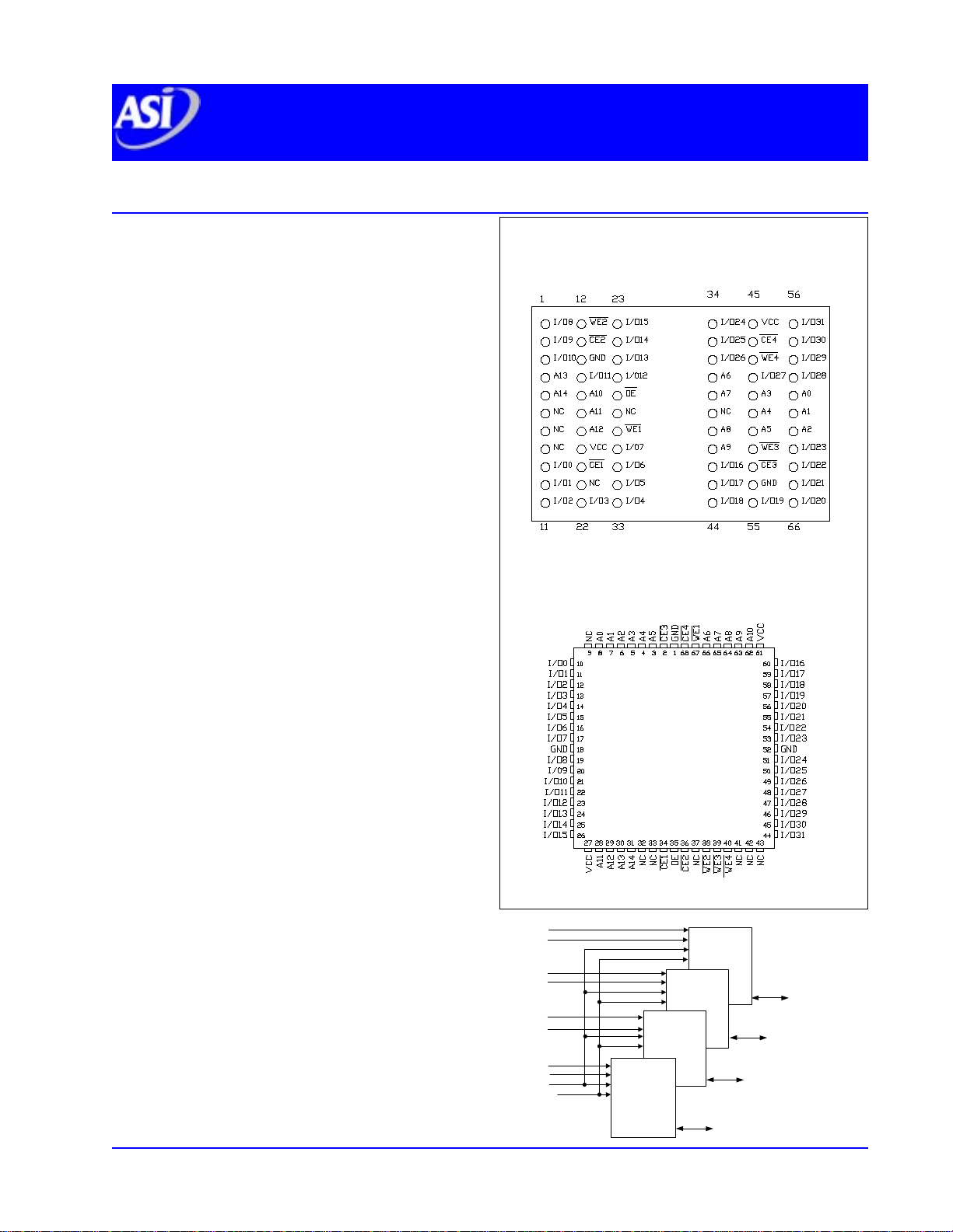
PIN ASSIGNMENT (Top V iew)
66 Lead PGA
68 Lead CQFP
GENERAL DESCRIPTION
The Austin Semiconductor, Inc. AS8E32K32 is a 1 Megabit
EEPROM Modules organized as 32K x 32 bit. User configurable to
64K x16 or 128Kx 8. The module achieves high speed access, low
power consumption and high reliability by employing advanced
CMOS memory technology.
The military grade product is manufactured in compliance to
the SMD and MIL-STD 883, making the AS8E32K32 ideally suited
for military or space applications.
The module is offered in a 1.090 sq inch ceramic pin grid array
substrate. This package design provides the optimum space saving
solution for boards that accept through hole packaging.
The module is also offered as a 68 lead 0.990 sq. inch ceramic
quad flatpack. It has a max. height of 0.200 inch. This package
design is targeted for those applications which require low profile
SMT Packaging.
DEVICE IDENTIFICA TION
An extra 64 bytes of EEPROM memory is available on each die
for user identification. By raising A9 to 12 V +/- 0.5V and using
address locations 7FC0H to 7FFFH the bytes may be written to
or read from in the same manner as the regular memory array.
AS8E32K32
REV. 1.5 9/99
CE4
WE4
CE3
WE3
CE2
WE2
32K x 8
CE1
WE1
OE
A0 - 14
1
M0
32K x 8
Austin Semiconductor, Inc., reserves the right to change products or specifications without notice.
M1
32K x 8
M2
32K x 8
M3
I/O 24 - I/O 31
I/O 16 - I/O 23
I/O 8 - I/O 23
I/O 0 - I/O 7
Page 2

AUSTIN SEMICONDUCTOR, INC.
AS8E32K32
32K x 32 EEPROM
DEVICE OPERATION
The 32Kx 32 EEPROM memory soultion is an electricaly erasable and programmable memory module that is accessed like a
Static RAM for the read or write cycle without the need for external components. The device contains a 64-byte-page register to
allow writing of up to 64 bytes of data simultaneously. During a write cycle, the address and 1 to 64 bytes of data are internally
latched, freeing the address and data bus for other operations. Following the initiation of a write cycle, the device will automatically
write the latched data using an internal control timer. The end of a write cycle can be detected by DATA polling of I/O7. Once the end
of a write cycle has been detected a new access for a read or write can begin.
READ
The memory module is accessed like a Static RAM. When
CE\ and OE\ are low and WE\ is High, the data stored at the
memory location determined by the address pins is asserted on
the outputs. The module can be read as a 32 bit, 16 bit or 8 bit
device. The outputs are put in the high impedance state when
either CE\ or OE\ is high. This dual-line control gives designers
flexibility in preventing bus contention in their system.
BYTE WRITE
A low pulse on the WE\ or CE\ input with CE\ or WE\ low
(respectively) and OE\ high initiates a write cycle. The address is
latched on the falling edge of CE\ or WE\, whichever occurs last.
The data is latched by the first rising edge of CE\ or WE\. Once a
BWDW (byte, word or double word) write has been started it
will automatically time itself to completion.
P AGE WRITE
The page write operation of the 32K x 32 EEPROM allows
1 to 64 BWDWs of data to be written into the device during a
single internal programming period. Each new BWDW must be
written within 150-µs (tBLC) of the previous BWDW. If the
tBLC limit is exceeded the device will cease accepting data and
commence the internal programming operation. For each WE
high to low transition during the page write operation, A6-A14
must be the same.
The A0-A5 inputs are used to specify which bytes within
the page are to be written. The bytes may be loaded in any order
and may be altered within the same load period. Only bytes
which are specified for writing will be written; unnecessary
cycling of other bytes within the page does not occur.
DA TA POLLING
this memory module features DATA Polling to indicate the
end of a write cycle. During a byte or page write cycle an
attempted read of the last byte written will result in the complement of the written data to be presented on I/O7. Once the write
cycle has been completed, true data is valid on all outputs, and
the next write cycle may begin. DATA Polling may begin at
anytime during the write cycle.
TOGGLE BIT
In addition to DATA Polling the module provides another
method for determining the end of a write cycle. During the write
operation, successive attempts to read data from the device will
result in I/O6 of the accessed die toggling between one and zero.
Once the write has completed, I/O6 will stop toggling and valid
data will be read. Reading the toggle bit may begin at any time
during the write cycle.
DA TA PROTECTION
If precautions are not taken, inadvertent writes may occur
during transitions of the host power supply. The E2 module has
incorporated both hardware and software features that will
protect the memory against inadvertent writes.
HARDW ARE PROTECTION
Hardware features protect against inadvertent writes to the
module in the following ways: (a) VCC sense - if VCC is below
3.8 V (typical) the write function is inhibited; (b) VCC power-on
delay - once VCC has reached 3.8 V the device will automatically
time out 5 ms (typical) before allowing a write; (c) write inhibit holding any one of OE\ low, CE\ high or WE\ high inhibits write
cycles; (d) noise filter - pulses of less than 15 ns (typical) on the
WE\ or CE\ inputs will not initiate a write cycle.
SOFTW ARE DA TA PROTECTION
A software controlled data protection feature has been
implemented on the memory module. When enabled, the
software data protection (SDP), will prevent inadvertent writes.
The SDP feature may be enabled or disabled by the user and is
shipped with SDP disabled.
SDP is enabled by the host system issuing a series of thre e
write commands; three specific bytes of data are written to three
specific addresses (refer to Software Data Protection Algorithm).
After writing the three byte command sequence and after tWC
the entire module will be protected from inadvertent write
operations. It should be noted, that once protected the host may
still perform a byte of page write to the module. This is done by
preceding the data to be written by the same three byte command
sequence used to enable SDP.
Once set, SDP will remain active unless the disable
command sequence is issued. Power transitions do not disable
SDP and SDP will protect the 32K x 32 EEPROM module during
power-up and Power-down conditions. All command sequences
must conform to the page write timing specifications. The data
in the enable and disable command sequences is not written to the
device and the memory addresses used in the sequence may be
written with data in either a byte of page write operation.
After setting SDP, any attempt to write to the device
without the three byte command sequence will start the internal
write timers. No data will be written to the device; however, for
the duration of tWC, read operations will effectively be polling
operations.
AS8E32K32
REV. 1.5 9/99
2
Austin Semiconductor, Inc., reserves the right to change products or specifications without notice.
Page 3
AUSTIN SEMICONDUCTOR, INC.
ELECTRICAL CHARACTERISTICS AND RECOMMENDED DC OPERATING CONDITIONS
MIN
-90
-120
NOTES
AS8E32K32
32K x 32 EEPROM
ABSOLUTE MAXIMUM RATINGS*
Voltage on Vcc Supply Relative to Vss
Vcc ..........................................................................-.6V to +6.5V
Storage T emperature ........................................-65°C to +150°C
Short Circuit Output Current (per I/O)….........................20mA
V oltage on any Pin Relative to Vss..............-.5V to Vcc+1 mA
Junction Temperature**..................................................+150 °C
Thermal Resistance junction to case (θ
):
JC
Package Type Q...........................................1 1.3° C/W
Package T ype P ..............................................2.8° C/W
(-55°C ≤ T A ≤ 125°C; Vcc = 5V ±10%)
DESCRIPTION CONDITIONS SYMBOL
Input High (Logic 1) Voltage
Input Low (Logic 0) Voltage
Input Leakage Current -10 10
Input Leakage Current
Output Leakage Current Output(s) disabled
Output High Voltage
Output Low Voltage
Supply Voltage
WE\, CE\
0V ≤ V
0V ≤ V
= -.4 mA V
I
OH
= 2.1mA V
I
OL
OUT
IN
≤ V
≤ V
CC
CC
*Stresses greater than those listed under "Absolute
Maximum Ratings" may cause permanent damage to the
device. This is a stress rating only and functional operation of the device at these or any other conditions above
those indicated in the operation section of this specification is not implied. Exposure to absolute maximum rating
conditions for extended periods may affect reliability .
** Maximum junction temperature depends upon package
type, cycle time, loading, ambient temperature and airflow ,
and humidity.
MAX UNITS NOTES
V
V
V
IH
IL
I
LI
I
LO
OH
OL
CC
2
-0.5 0.8 V 1, 2
-10 10
-10 10
2.4 V 1
4.5 5.5 V 1
V
CC
0.45 V 1
+.3
V 1
µA
µA
µA
DESCRIPTION CONDITIONS SYMBOL
Power Supply
CE\ ≤ V
Current: Operating f = 5 MHz
; VCC = MAX
IL
I
OUTPUTS OPEN
Power Supply
Current: Standby
CE\ ≥ V
≤V
; All Other Inputs
IH
or ≥ VIH; VCC = MAX I
IL
SBT1
f = 5 MHz
AS8E32K32
REV. 1.5 9/99
CE\ ≥ V
V
IH
-0.2V; V
CC
V
≤ VSS +0.2V or
IL
CC
= MAX
≥ VCC -0.2V; f = 0 Hz
I
SBC1
3
CC
MAX
-150 UNITS
340 340 340 mA
12 12 12 mA
1.3 1.3 1.3 mA
Austin Semiconductor, Inc., reserves the right to change products or specifications without notice.
Page 4
AUSTIN SEMICONDUCTOR, INC.
MODE
AS8E32K32
32K x 32 EEPROM
)1(
ELBATECNATICAPAC
V
NI
lobmySretemaraPmumixaMstinUsetoN
Cº52=AT,zHM1=f,V0=
C
DDA
C
EO
C,
C
EW
EC
C
OI
1. This parameter is guaranteed but not tesed
ecnaitcapaC41A-0A42Fp41,4
ecnaitcapaC\EO42Fp41,4
ecnaitcapaC\ECdna\EW6Fp41,4
ecnaitcapaC13O/I-0O/I21Fp41,4
TRUTH TABLE
CE\ OE\ WE\ I/O
Read
Write (2)
Standby/Write
V
IL
V
IL
V
IH
X (1) X High Z
Write Inhibit X X
Write Inhibit X
Output Disable X
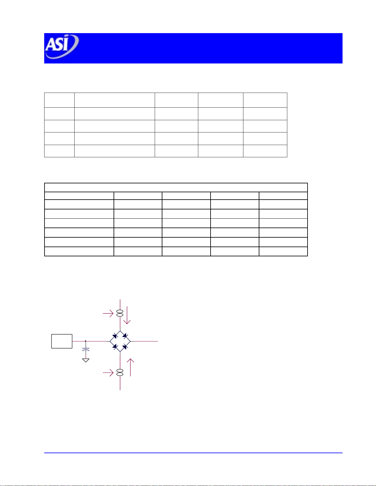
AC TEST CONDITIONS
V
IL
V
IH
V
IL
V
IH
V
IH
V
IL
V
IH
D
OUT
D
X
X High Z
IN
I
OL
Current Source
Device
Under
Test
Ceff = 50pf
Current Source
+
-+
I
OH
Vz = 1.5V
(Bipolar
Supply)
Notes:
Vz is programable from -2V to + 7V .
IOL and IOH programmable from 0 to 16 mA.
Vz is typically the midpoint of VOH and VOL.
IOL and IOH are adjusted to simulate a typical resistive load
circuit.
AS8E32K32
REV. 1.5 9/99
T est Specifications
Input pulse levels....................................VSS to 3V
Input rise and fall times.......................................5ns
Input timing reference levels.............................1.5V
Output reference levels.....................................1.5V
Output load................................See Figures 1 and 2
4
Austin Semiconductor, Inc., reserves the right to change products or specifications without notice.
Page 5

AUSTIN SEMICONDUCTOR, INC.
tACC
tOHtOE
tDFtCE
tRCtRC
OUTPUT VALID
ADDRESS VALID
ADDRESS
CE/
OE\
DQ
Symbol
Max
AC READ CHARACTERISTICS
(-55°C ≤ T A ≤ 125°C; VCC = 5V ±10%)
Parameter
t
t
t
t
t
t
t
RC
ACC
ACS
CE
OE
DF
OH
(3,4)
(1)
(2)
Read Cycle Time
Address to Output Delay
CE\ Access Time
CE\ to Output Delay
OE\ to Output Delay
CE\ or OE\ to Output High-Z
Output Hold from OE\, CE\ or
Address, whichever occurs first
AS8E32K32
32K x 32 EEPROM
-90 -120 -150
Min Max Min
90 120 150
90 120 150
90 120 150
90 120 150
50 60 70
50 60 70
Min Max
Units
ns
ns
ns
ns
ns
ns
0
ns00
A.C. Read W aveforms
(1,2,3)
Notes:
1. CE\ may be delayed to t
after the address transition without inpact on t
ACC-tCE
ACC
.
2. OE\ may be delayed to tCE-tOE after the falling edge of CE\ without inpact on tCE or by t
without inpact on t
ACC
.
3. tDF is specified from OE\ or CE\ whichever occurs first (CL = 5pF).
after an address change
ACC-tOE
AS8E32K32
REV. 1.5 9/99
5
Austin Semiconductor, Inc., reserves the right to change products or specifications without notice.
Page 6

AUSTIN SEMICONDUCTOR, INC.
tDH
tDS
tWPHtWPHtWPtWP
tCHtCS
tWC
tAH
tWC
tAS
tOEHtOES
DATA VALID
ADDRESS VALID
OE\
ADDRESS
WE\
CE\
DQ
AS8E32K32
32K x 32 EEPROM
AC WRITE CHARACTERISTICS
(-55°C ≤ T A ≤ 125°C; VCC = 5V ±10%)
-90 -120 -150
Symbol Parameter Min Max Min Max Min Max Unit
t
wc
t
AS
t
AH
t
CS
t
CH
t
WP
t
DS
t
DH
t
t
OES
t
WPH
OEH
Write Cycle Time 10 10 10 ms
Address, OE\ Set-Up time 0 0 0 ns
Address, Hold time 50 50 50 ns
Chip Select Set-up Time 0 0 0 ns
Chip Select Hold Time 0 0 0 ns
Write Pulse Width (WE\ or CE\) 100 100 100 ns
Data Set-up Time 50 50 50 ns
Data Hold Time 0 0 0 ns
OE\ Hold time 0 0 0 ns
OE\ Set-up time 0 0 0 ns
Write Pulse Width High 50 50 50 ns
WRITE CYCLE NO 1.
(Chip Enable Controlled)
AS8E32K32
REV. 1.5 9/99
6
Austin Semiconductor, Inc., reserves the right to change products or specifications without notice.
Page 7

OE\
ADDRESS
CE\
WE\
DQ
AUSTIN SEMICONDUCTOR, INC.
WRITE CYCLE NO 2.
(Write Enable Controlled)
tAH
tAS
tDS
DATA VALID
AS8E32K32
32K x 32 EEPROM
tOEHtOES
tCHtCS
tWPHtWPHtWPtWP
tDH
AS8E32K32
REV. 1.5 9/99
7
Austin Semiconductor, Inc., reserves the right to change products or specifications without notice.
Page 8

AUSTIN SEMICONDUCTOR, INC.
PAGE MODE CHARACTERISTICS
(-55°C ≤ T A ≤ 125°C; VCC = 5V ±10%)
Symbol Parameter Min Max Min Max Min Max Unit
t
wc
Write Cycle Time 0 0 0 ms
t
WP
Write Pulse Width (WE\ or CE\) 100 100 100 ns
t
DS
Data Set-up Time 50 50 50 ns
t
DH
Data Hold Time 0 0 0 ns
t
BLC
Byte Load Cycle Time 150 150 150
µ
s
t
WPH
Write Pulse Width High 50 50 50 ns
-90 -120 -150
AS8E32K32
32K x 32 EEPROM
Page Mode Write W aveforms
(1,2)
OE
CE\
tBLCtBLCtWPHtWPHtWPtWP
WE\
tAH
tAS
A0 - A16
VA VA VAVAVA VA
tDH
tDS
DATA
VD VD VD VD VD
BYTE 0 BYTE 1 BYTE 2 BYTE 3 BYTE127BYTE 126
Notes: 1. A7 through A16 must specify the page address during each high to low transition of WE\ (or CE\).
2. OE\ must be high only when WE\ and CE\ are both low.
3. VD - Valid Data
4. VA - Valid Address
VA
tWC
VD VD
VDVD
AS8E32K32
REV. 1.5 9/99
8
Austin Semiconductor, Inc., reserves the right to change products or specifications without notice.
Page 9

AUSTIN SEMICONDUCTOR, INC.
AS8E32K32
32K x 32 EEPROM
Software Data Protection Enable Algorithm
Load Data AA
to
Address 5555
Load Data 55
to
Address 2AAA
Load Data A0
to
Address 5555
Load Data XX
to
Any Address
Load Last Byte
to
Last Address
Writes Enabled
(4)
Enter Data
Protect State
(1)
Software Data Protection Disable Algorithm
(1)
Load Data AA
to
Address 5555
Load Data 55
to
Address 2AAA
(2)
Load Data 80
to
Address 5555
Load Data AA
to
Address 5555
Load Data 20
to
Address 5555
Exit Data Protect
(3)
State
Load Data XX
to
Any Address
(4)
Load Last Byte
to
Last Address
Notes:
1. Data Format: I/O 7 - I/O 0, I/O 15 - I/O 8, I/O 23 - I/O 16, and I/O 31 - I/O 24, (Hex)
2. Write Protect state will be active at end of write even if no other data is loaded.
3. Write Protect state will be deactivated at end of period even if no other data is loaded.
4. 1 to 64 bytes of data are loaded.
5. A0-A12 of the selected I/O bytes must conform to the addressing sequence for the first three bytes as shown above.
6. After the command sequence has been issued and a page write operation follows, the page address inputs (A5-A14) of the selected I/O
bytes must be the same for each high to low transition of WE\ (or CE\).
7. OE Must be high only when WE\ and CE\ are both low.
AS8E32K32
REV. 1.5 9/99
9
Austin Semiconductor, Inc., reserves the right to change products or specifications without notice.
Page 10

AUSTIN SEMICONDUCTOR, INC.
Symbol Parameter Min Max Units
t
DH
Data Hold Time 10 ns
t
OEH
OE\ Hold Time 10 ns
t
OE
OE\ to Output Delay
(2)
100 ns
t
WR
Write Recovery Time 0 ns
AS8E32K32
32K x 32 EEPROM
Data Polling Characteristics
(1)
Notes: 1. These parameters are characterized and not 100% tested.
2. See A.C. Read Characteristics.
Data Polling Waveforms
tOEH
WE\
CE\
tDH
OE\
I/O 7
A0 - A17
VA VA VA VA VAVA
tWRtOE
T oggle Bit Characteristics
(1)
Symbol Parameter Min Max Units
t
DH
t
OEH
t
OE
t
OEPH
I
CC
Notes: 1. These parameters are characterized and not 100% tested.
2. See A.C. Read Characteristics.
Toggle Bit Waveforms
Data Hold Time 10 ns
OE\ Hold Time 10 ns
OE\ to Output Delay
OE\ High Pulse 150 ns
Write Recovery Time 0 ns
(1,2,3)
(2)
100 ns
WE\
CE\
tOEH
OE\
HIGH Z
I/O 6
Notes: 1. Toggling either OE or CE or Both OE and CE will operate toggle bit.
2. Beginning and ending state of I/O6 will vary.
3. Any address location may be used but the address should not vary.
AS8E32K32
REV. 1.5 9/99
10
Austin Semiconductor, Inc., reserves the right to change products or specifications without notice.
tWRtWRtOEtDH
Page 11

AUSTIN SEMICONDUCTOR, INC.
MECHANICAL DEFINITION
AS8E32K32
(ASI Case #705, Package Designator Q)
AS8E32K32
32K x 32 EEPROM
AS8E32K32
REV. 1.5 9/99
11
Austin Semiconductor, Inc., reserves the right to change products or specifications without notice.
Page 12

AUSTIN SEMICONDUCTOR, INC.
MECHANICAL DEFINITION
AS8E32K32
(ASI Case #805, Package Designator P)
AS8E32K32
32K x 32 EEPROM
AS8E32K32
REV. 1.5 9/99
12
Austin Semiconductor, Inc., reserves the right to change products or specifications without notice.
 Loading...