

Datasheet AS7C31026A-20TI, AS7C31026A-20TC, AS7C31026A-20JC, AS7C31026A-20BI, AS7C31026A-20BC Datasheet (Alliance Semiconductor Corporation)
...Page 1
January 2001
Advance Information
Copyright © Alliance Semiconductor. All rights reserved.
®
AS7C1026A
AS7C31026A
5V/3.3V 64K X 16 CMOS SRAM
2/6/01; V.0.9 Alliance Semiconductor P. 1 of 9
Features
• AS7C1026A (5V version)
• AS7C31026A (3.3V version)
• Industrial and commercial versions
• Organization: 65,536 words × 16 bits
• Center power and ground pins for low noise
• High speed
- 10/12/15/20 ns address access time
- 3/3/4/5 ns output enable access time
• Low power consumption: ACTIVE
- 660 mW (AS7C1026A) / max @ 10 ns
- 324 mW (AS7C31026A) / max @ 10 ns
• Low power consumption: STANDBY
- 55 mW (AS7C1026A) / max CMOS I/O
- 36 mW (AS7C31026A) / max CMOS I/O
• Latest 6T 0.25u CMOS technology
• 2.0V data retention
• Easy memory expansion with CE
, OE inputs
• TTL-compatible, three-state I/O
• JEDEC standard packaging
- 44-pin 400 mil SOJ
- 44-pin 400 mil TSOP II
- 48-ball 6 mm × 8 mm CSP mBGA
• ESD protection ≥ 2000 volts
• Latch-up current ≥ 200 mA
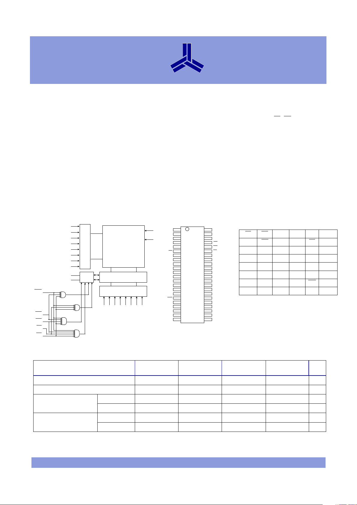
Logic block diagram
64K × 16
Array
OE
CE
WE
Column decoder
Row decoder
A0
A1
A2
A3
A4
A5
A7
V
CC
GND
A8
A9
A10
A11
A12
A13
A14
A15
Control circuit
I/O0–I/O7
I/O8–I/O15
UB
LB
I/O
buffer
A6
Pin arrangement
5
6
7
8
9
10
11
12
13
14
15
16
17
18
19
20
I/O13
I/O12
GND
V
CC
I/O11
I/O10
I/O9
I/O8
NC
A8
A9
A10
A11
NC
A0
CE
I/O0
I/O1
I/O2
I/O3
V
CC
GND
I/O4
I/O5
I/O6
I/O7
WE
A15
A14
A13
44-Pin SOJ, TSOP II (400 mil)
21
22
A12
NC
UB
LB
I/O15
I/O14
2
A3
3
A2
4
A1
1
A4
40
39
38
37
36
35
34
33
32
31
30
29
28
27
26
25
24
23
43
42
41
44
A6
A7
OE
A5
AS7C1026A
AS7C31026A
Selection guide
AS7C1026A-10
AS7C31026A-10
AS7C1026A-12
AS7C31026A-12
AS7C1026A-15
AS7C31026A-15
AS7C1026A-20
AS7C31026A-20 Unit
Maximum address access time
10 12 15 20 ns
Maximum output enable access time
3345ns
Maximum operating current
AS7C1026A 120 110 100 100 mA
AS7C31026A 90 80 80 80 mA
Maximum CMOS standby
current
AS7C1026A 10 10 10 15 mA
AS7C31026A 10 10 10 15 mA
48-CSP mini Ball-Grid-Array Package
123456
ALB
OE A
0
A1A2NC
BI/O8 UB
A3 A4 CE I/O0
CI/O9
I/O10
A5 A6 I/O1 I/O2
DV
SS
I/O11
NC A7 I/O3 V
DD
EVDDI/O12
NC NC I/O4 V
SS
FI/O14
I/O13
A14 A15 I/O5 I/O6
GI/O15 NC A12 A13 WE
I/O7
HNC A8 A9A10A11NC
Page 2
®
AS7C1026A
AS7C31026A
2/6/01; V.0.9 Alliance Semiconductor P. 2 of 9
Functional description
The AS7C1026A and AS7C31026A are high-performance CMOS 1,048,576-bit Static Random Access Memory (SRAM) devices organized as
65,536 words × 16 bits. They are designed for memory applications where fast data access, low power, and simple interfacing are desired.
Equal address access and cycle times (t
AA
, tRC, tWC) of 10/12/15/20 ns with output enable access times (tOE) of 3/3/4/5 ns are ideal for
high-performance applications.
When CE
is high the devices enter standby mode. The AS7C1026A is guaranteed not to exceed 55 mW power consumption in CMOS
standby mode. The devices also offer 2.0V data retention.
A write cycle is accomplished by asserting write enable (WE
) and chip enable (CE). Data on the input pins I/O0–I/O15 is written on the
rising edge of WE
(write cycle 1) or CE (write cycle 2). To avoid bus contention, external devices should drive I/O pins only after outputs
have been disabled with output enable (OE
) or write enable (WE).
A read cycle is accomplished by asserting output enable (OE) and chip enable (CE), with write enable (WE) high. the chips drive I/O pins
with the data word referenced by the input address. When either chip enable or output enable is inactive, or write enable is active, output
drivers stay in high-impedance mode.
The devices provide multiple center power and ground pins, and separate byte enable controls, allowing individual bytes to be written and
read. LB
controls the lower bits, I/O0–I/O7, and UB controls the higher bits, I/O8–I/O15.
All chip inputs and outputs are TTL-compatible, and operation is from a single 5V supply (AS7C1026A) or 3.3V supply (AS7C31026A). the
device is packaged in common industry standard packages. Chip scale BGA packaging, easy to use in manufacturing, provides the smallest
possible footprint. This 48-ball JEDEC-registered package has a ball pitch of 0.75 mm and external dimensions of 8 mm × 6 mm.
Absolute maximum ratings
Note: Stresses greater than those listed under Absolute Maximum Ratings may cause permanent damage to the device. This is a stress rating only and functional
operation of the device at these or any other conditions outside those indicated in the operational sections of this specification is not implied. Exposure to
absolute maximum rating conditions for extended periods may affect reliability.
Truth table
Key:
H = High, L = Low, X = don’t care.
Parameter Symbol Min Max Unit
Vol t ag e o n V
CC
relative to GND
AS7C1026A V
t1
–0.50 +7.0 V
AS7C31026A V
t1
–0.50 +5.0 V
Voltage on any pin relative to GND Both V
t2
–0.50 VCC +0.50 V
Power dissipation Both P
D
–1.0W
Storage temperature (plastic) Both T
stg
–65 +150 °C
Ambient temperature with VCC
applied
Both T
bias
–55 +125 °C
DC current into outputs (low) Both I
OUT
–20mA
CE
WE OE LB UB I/O0–I/O7 I/O8–I/O15 Mode
H X X X X High Z High Z Standby (I
SB
), I
SBI
)
LHLLHD
OUT
High Z Read I/O0–I/O7 (ICC)
LHLHLHigh ZD
OUT
Read I/O8–I/O15 (I
CC)
LHLL LD
OUT
D
OUT
Read I/O0–I/O15 (ICC)
LLXLLD
IN
D
IN
Write I/O0–I/O15 (ICC)
LLXLHD
IN
High Z Write I/O0–I/O7 (ICC)
LLXHLHigh ZD
IN
Write I/O8–I/O15 (ICC)
L
L
H
X
H
X
X
H
X
H
High Z High Z Output disable (I
CC
)
Page 3
®
AS7C1026A
AS7C31026A
2/6/01; V.0.9 Alliance Semiconductor P. 3 of 9
Recommended operating conditions
†
VIL min. = –3.0V for pulse width less than tRC/2.
DC operating characteristics (over the operating range)
1
Capacitance (f = 1MHz, T
a
= 25 °C, V
CC
= NOMINAL)
2
Parameter Device Symbol Min Nominal Max Unit
Supply voltage
AS7C1026A V
CC
4.5 5.0 5.5 V
AS7C31026A V
CC
3.0 3.3 3.6 V
Input voltage
AS7C1026A V
IH
2.2 – VCC + 0.5 V
AS7C31026A V
IH
2.0 – VCC + 0.5 V
Both V
IL
†
–0.5 – 0.8 V
Ambient operating temperature
commercial T
A
0– 70
o
C
industrial T
A
–40 – 85
o
C
Parameter Sym Test conditions Device
-10 -12 -15 -20
UnitMin Max Min Max Min Max Min Max
Input leakage
current
| ILI |
VCC = Max
V
IN
= GND to V
CC
Both – 1 – 1 – 1 – 1 µA
Output leakage
current
| I
LO
|
V
CC
= Max
CE
= VIH,
V
OUT
= GND to V
CC
Both – 1 – 1 – 1 – 1 µA
Operating power
supply current
I
CC
V
CC
= Max, CE ≤ V
IL
outputs open,
f = f
Max
= 1/t
RC
AS7C1026A – 120 – 110 – 100 – 100 mA
AS7C31026A – 90 – 80 – 80 – 80 mA
Standby
power supply
current
I
SB
VCC = Max, CE
≤ V
IL
,
outputs open,
f = f
Max
= 1/t
RC
AS7C1026A – 30 – 25 – 20 – 20
mA
AS7C31026A – 30 – 25 – 20 – 20
I
SB1
V
CC
= Max, CE ≥ V
CC
–0.2V,
V
IN
≤ GND + 0.2V or
V
IN
≥ V
CC
–0.2V, f = 0
AS7C1026A – 10 – 10 – 10 – 15
mA
AS7C31026A – 10 – 10 – 10 – 15
Output
voltage
V
OL
IOL = 8 mA, VCC = Min AS7C1026A – 0.4 – 0.4 – 0.4 – 0.4 V
V
OH
IOH = –4 mA, VCC = Min AS7C31026A 2.4 – 2.4 – 2.4 – 2.4 – V
Data retention
current
I
CCDR
VCC = 2.0V
CE
≥ V
CC
–0.2V
V
IN
≥ V
CC
–0.2V or
V
IN
≤ 0.2V
AS7C1026A
11 1 5mA
AS7C31026A
11 1 5mA
Parameter Symbol Signals Test conditions Max Unit
Input capacitance C
IN
A, CE, WE, OE, LB, UB VIN = 0V 5 pF
I/O capacitance C
I/O
I/O VIN = V
OUT
= 0V 7 pF
Page 4

®
AS7C1026A
AS7C31026A
2/6/01; V.0.9 Alliance Semiconductor P. 4 of 9
Read cycle (over the operating range)
3,9
Key to switching waveforms
Read waveform 1 (address controlled)
3,6,7,9
Read waveform 2 (OE, CE, UB, LB controlled)
3,6,8,9
Parameter Symbol
-10 -12 -15 -20
Unit NotesMinMaxMinMaxMinMaxMinMax
Read cycle time t
RC
10 – 12 – 15 – 20 – ns
Address access time t
AA
–10–12–15–20ns 3
Chip enable (CE
) access time t
ACE
–10–12–15–20ns 3
Output enable (OE
) access time t
OE
–3–3–4–5ns
Output hold from address change t
OH
2–3–3–3–ns 5
CE
Low to output in low Z t
CLZ
0–0–0–0–ns4, 5
CE
High to output in high Z t
CHZ
–3–3–4–5ns4, 5
OE
Low to output in low Z t
OLZ
0–0–0–0–ns4, 5
Byte select access time t
BA
–3–3–4–5ns
Byte select Low to low Z t
BLZ
0–0–0–0–ns4, 5
Byte select High to high Z t
BHZ
–5–6–6–8ns4, 5
OE
High to output in high Z t
OHZ
–3–3–4–5ns4, 5
Power up time t
PU
0–0–0–0–ns4, 5
Power down time t
PD
–10–12–15–20ns4, 5
Undefined output/don’t careFalling inputRising input
t
OH
t
AA
t
RC
t
OH
Data
OUT
Address
Data validPrevious data valid
Data valid
t
RC
t
AA
t
BLZ
t
BA
t
OE
t
OLZ
t
OH
t
OHZ
t
HZ
t
BHZ
t
ACE
t
LZ
Address
OE
CE
LB, UB
Data
IN
Page 5

®
AS7C1026A
AS7C31026A
2/6/01; V.0.9 Alliance Semiconductor P. 5 of 9
Write cycle (over the operating range)
11
Write waveform 1 (WE controlled)
10,11
Write waveform 2 (CE controlled)
10,11
Parameter Symbol
-10 -12 -15 -20
Unit NotesMin Max Min Max Min Max Min Max
Write cycle time t
WC
10 – 12 – 15 – 20 – ns
Chip enable (
CE
) to write end t
CW
8 – 10 – 12 – 12 – ns
Address setup to write end t
AW
8 – 9 – 10 – 12 – ns
Address setup time t
AS
0–0–0 –0– ns
Write pulse width t
WP
7–8–9–12– ns
Address hold from end of write t
AH
0–0–0 –0– ns
Data valid to write end t
DW
5–6–8–10– ns
Data hold time t
DH
0–0–0 –0– ns 5
Write enable to output in high Z t
WZ
– 6 – 6 – 6 – 8 ns 4, 5
Output active from write end t
OW
1–1–1 –2– ns 4, 5
Byte select low to end of write t
BW
8 – 10 – 12 – 12 – ns
Address
CE
LB, UB
WE
Data
IN
Data
OUT
t
WC
t
CW
t
BW
t
AW
t
AS
t
WP
t
DW
t
DH
t
OW
t
WZ
t
WR
Data undefined
high Z
Data valid
Address
CE
LB, UB
WE
Data
IN
t
WC
t
CW
t
BW
t
WP
t
DW
t
DH
t
OW
t
WZ
t
WR
Data
OUT
Data undefined
high Z high Z
t
AS
t
AW
Data valid
t
CLZ
Page 6

AS7C1026A
AS7C31026A
®
2/6/01 Alliance Semiconductor P. 6 of 9
Data retention characteristics (over the operating range)
Data retention waveform
AC test conditions
Notes
1During VCC power-up, a pull-up resistor to VCC on CE is required to meet ISB specification.
2 This parameter is sampled, but not 100% tested.
3 For test conditions, see AC Test Conditions, Figures A, B, and C.
4 These parameters are specified with C
L
= 5pF, as in Figures B or C. Transition is measured ± 500 mV from steady-state voltage.
5 This parameter is guaranteed, but not tested.
6WE
is High for read cycle.
7CE
and OE are Low for read cycle.
8 Address valid prior to or coincident with CE
transition Low.
9 All read cycle timings are referenced from the last valid address to the first transitioning address.
10 CE
or WE must be High during address transitions. Either CE or WE asserting high terminates a write cycle.
11 All write cycle timings are referenced from the last valid address to the first transitioning address.
12 Not applicable.
13 C=30pF, except all high Z and low Z parameters where C=5pF.
Parameter Symbol Test conditions Min Max Unit
V
CC
for data retention V
DR
VCC = 2.0V
CE
≥ V
CC
–0.2V
V
IN
≥ V
CC
–0.2V or
V
IN
≤ 0.2V
2.0 – V
Data retention current I
CCDR
–1 ma
Chip deselect to data retention time t
CDR
0–ns
Operation recovery time t
R
t
RC
–ns
Input leakage current |I
LI
|–1µA
V
CC
CE
t
R
t
CDR
Data retention mode
V
CC
V
CC
V
DR
≥
2.0V
V
IH
V
IH
V
DR
255W C(14)
320W
GND
+3.3V
Figure C: 3.3V Output load
168W
Thevenin Equivalent:
D
OUT
+1.728V (5V and 3.3V)
255W
C(14)
480W
GND
+5V
Figure B: 5V Output load
10%
90%
10%
90%
GND
+3.0V
Figure A: Input pulse
2 ns
D
OUT
D
OUT
– Output load: see Figure B or Figure C.
– Input pulse level: GND to 3.0V. See Figure A.
– Input rise and fall times: 2 ns. See Figure A.
– Input and output timing reference levels: 1.5V.
Page 7

®
AS7C1026A
AS7C31026A
2/6/01; V.0.9 Alliance Semiconductor P. 7 of 9
Package dimensions
44-pin TSOP II
Min
(mm)
Max
(mm)
A1.2
A1 0.05
A2 0.95 1.05
b
0.30
0.45
c 0.127 (typical)
D 18.28 18.54
E
10.03
10.29
He 11.56 11.96
e 0.80 (typical)
l0.400.60
D
He
1234567891011121314
44 43 4241 40 39 38 37 36 35 34 33 32 31
15 16
30 29
17 18 19 20
28 27 26 25
c
l
A1
A2
e
44-pin TSOP II
0–5
°
212422
23
E
A
b
Seating
Plane
44-pin SOJ
44-pin SOJ
400 mil
Min (in) Max (in)
A 0.128 0.148
A
1
0.025 –
A
2
0.105 1.115
B 0.026 0.032
b 0.015 0.020
c 0.007 0.013
D 1.120 1.130
E 0.370 NOM
E
1
0.395 0.405
E
2
0.435 0.445
e 0.050 NOM
e
Pin 1
A
1
b
B
A
A
2
E
2
E
1
E
2
D
c
Page 8

AS7C1026A
AS7C31026A
®
2/6/01 Alliance Semiconductor P. 8 of 9
Notes
1 Bump counts: 48 (8 row x 6 column).
2 Pitch: (x,y) = 0.75 mm x 0.75 mm (typ).
3 Units: millimeters.
4 All tolerance are +/- 0.050 unless otherwise
specified.
5 Typ: typical.
6 Y is coplanarity: 0.08 (max).
Minimum Typical Maximum
A–0.75–
B 5.90 8.00 8.10
B1 – 3.75 –
C 7.90 8.00 8.10
C1 – 5.25 –
D–0.35–
E––1.20
E1 – 0.68 –
E2 0.22 0.25 0.27
Y––0.08
48-ball FBGA
Bottom View
6543 2 1
Ball A1
C1
A
B
C
D
F
G
H
J
A
B1
Side View
Top V i ew
Ball #A1 index
C
SRAM DIE
Elastomer
B
Detail View
A
Y
Die
0.3/T
µ
p
E2
E
Die
D
E1
E2
E
*pin 1 indicator will show as
engraved circle and/or Inc. trade mark
*
Page 9

®
AS7C1026A
AS7C31026A
© Copyright Alliance Semiconductor Corporation. All rights reserved. Our three-point logo, our name and Intelliwatt are trademarks or registered tr ademarks of Allia nce . All o the r br an d an d
product names may be the trademarks of their respective companies. Alliance reserves the right to m ak e ch an ges to th is d ocu m e nt an d its pr od u cts at a ny tim e with ou t notic e. Allia nce assum es no
responsibility for any errors that may app ear in th is doc um e nt. T h e d ata c ontain ed h ere in re pr esent s Allian ce ’s best data a nd /or e stim ate s at the ti me of issuan ce. Al lianc e reser ves the righ t to
change or correct this data at any time, without notice. If the product described herein is under development, significant changes to these specificatio ns are pos sible. Th e in fo rm atio n in th is
product data sheet is intended to be general descriptive information for potential customers and users, and is not intended to operate as, or provide, any guarantee or warrantee to any user or
customer. A llian ce d oe s no t assum e any respo n sibility or liability arisi ng o ut o f th e ap plic ation or use o f any product described herein, and disclaims any express or implied warranties related to
the sale and/or use o f A llianc e pr o duc ts inclu din g liab ility o r w arra ntie s related to fitn ess fo r a p articu lar p urp ose, m erc han tabi lity , or infrin ge me n t of a ny int ellectua l pr op erty righ ts, ex cep t as
express agreed to in A llian ce’s T erm s an d C on ditio n s of Sale (which are availa ble from Alliance). A ll sales o f A llian ce pr o duc ts are m ad e e xclus ively acco rdin g to Allia nc e’s Te rm s and
Conditions of Sale. The purchase of products from Alliance does not convey a license under any patent rights, copyrights, mask works rights, trademarks, or any other intellectual property rights
of Alliance o r third pa rties. A llian ce doe s no t au thoriz e its pr oducts for use as critical components in life-supporting systems where a malfunction or failure may reasonably be expected to result
in significant inju ry to the u ser, a nd the in clu sion o f A llia nce pro d ucts in such lif e- supporting systems implies that the manufacturer assumes all risk of such use and agrees to indemnify Alliance
against all claims arising from such use.
2/6/01; V.0.9 Alliance Semiconductor P. 9 of 9
Ordering codes
Part numbering system
Package \ Access time Volt/Temp 10 ns 12 ns 15 ns 20 ns
Plastic SOJ, 400 mil
5V commercial AS7C1026A-10JC AS7C1026A-12JC AS7C1026A-15JC AS7C1026A-20JC
5V industrial AS7C1026A-10JI AS7C1026A-12JI AS7C1026A-15JI AS7C1026A-20JI
3.3V commercial AS7C31026A-10JC AS7C31026A-12JC AS7C31026A-15JC AS7C31026A-20JC
TSOP II, 18.4×10.2
mm
5V commercial AS7C1026A-10TC AS7C1026A-12TC AS7C1026A-15TC AS7C1026A-20TC
3.3V commercial AS7C31026A-10TC AS7C31026A-12TC AS7C31026A-15TC AS7C31026A-20TC
3.3V industrial AS7C31026A-10TI AS7C31026A-12TI AS7C31026A-15TI AS7C31026A-20TI
CSP BGA, 8×6 mm
5V commercial AS7C1026A-10BC AS7C1026A-12BC AS7C1026A-15BC AS7C1026A-20BC
3.3V commercial AS7C31026A-10BC AS7C31026A-12BC AS7C31026A-15BC AS7C31026A-20BC
3.3V industrial AS7C31026A-10BI AS7C31026A-12BI AS7C31026A-15BI AS7C31026A-20BI
AS7C X 1026 –XX X C
SRAM
prefix
Blank=5V CMOS
3=3.3V CMOS
Device
number
Access
time
Package: J=SOJ 400 mil
T=TSOP type 2, 18.4 × 10.2 mm
B=CSP BGA, 8 × 6 mm
Temperature range,
C= Commercial: 0° C to 70° C
I= Industrial: -40° C to 85° C
 Loading...