

Datasheet AS7C31024A-20TJI, AS7C31024A-20TJC, AS7C31024A-20TI, AS7C31024A-20TC, AS7C31024A-20JI Datasheet (Alliance Semiconductor Corporation)
...Page 1
January 2001
Advance Information
5V/3.3V 128KX8 CMOS SRAM (Evolutionary Pinout)
Features
• AS7C1024A (5V version)
• AS7C31024A (3.3V version)
• Industrial and commercial temperatures
• Organization: 131,012 words x 8 bits
• High speed
- 10/12/15/20 ns address access time
- 3/3/4/5 ns output enable access time
• Low power consumption: ACTIVE
- 660 mW (AS7C1024A) / max @ 10 ns
- 324 mW (AS7C31024A) / max @ 10 ns
• Low power consumption: STANDBY
- 55 mW (AS7C1024A) / max CMOS
- 36 mW (AS7C31024A) / max CMOS
AS7C1024A
AS7C31024A
®
• Latest 6T 0.25u CMOS technology
• 2.0V data retention
• Easy memory expansion with CE1
• TTL/LVTTL-compatible, three-state I/O
• 32-pin JEDEC standard packages
-300 mil SOJ
-400 mil SOJ
- 8 × 20mm TSOP I
• ESD protection ≥ 2000 volts
• Latch-up current ≥ 200 mA
, CE2, OE inputs
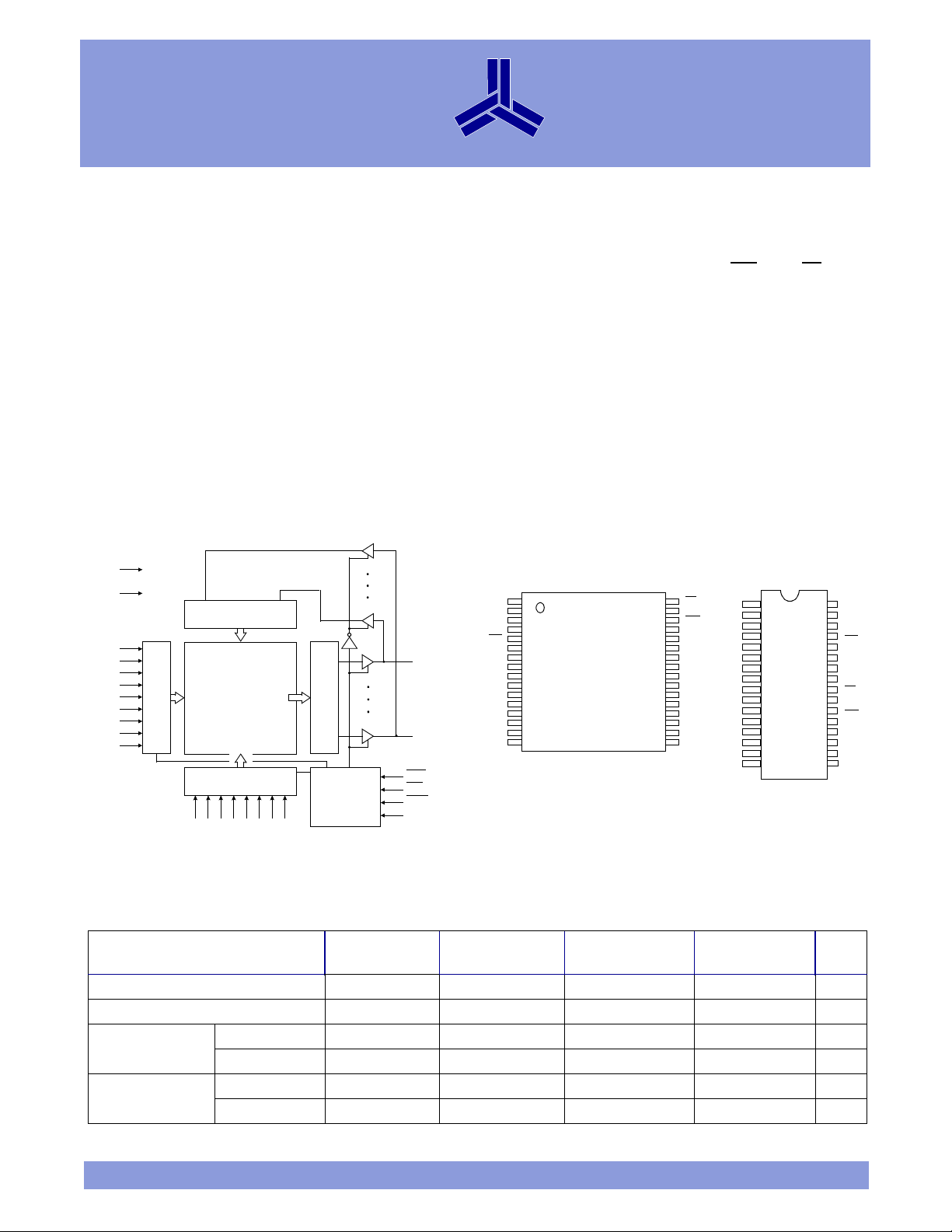
Logic block diagram
V
CC
GND
Input buffer
A0
A1
A2
A3
A4
A5
A6
A7
A8
Row decoder
512×256×8
(1,048,576)
Column decoder
A9
A10
A11
Array
A12
I/O7
Sense amp
I/O0
Control
circuit
A13
A14
A15
A16
WE
OE
CE1
CE2
Pin arrangement
32-pin TSOP I
(8 x 20mm)
A11 OE
1
2
A9
3
A8
4
A13
5
WE
6
CE2
7
A15
8
V
CC
9
NC
10
A16
11
A14
12
A12
13
A7
14
A6
15
A5
16
A4 A3
AS7C1024A
AS7C31024A
32
31
30
29
28
27
26
25
24
23
22
21
20
19
18
17
A10
CE1
I/O7
I/O6
I/O5
I/O4
I/O3
GND
I/O2
I/O1
I/O0
A0
A1
A2
32-pin SOJ (300 mil)
32-pin SOJ (400 mil)
NC
A16
A14
A12
A7
A6
A5
A4
A3
A2
A1
A0
I/O0
I/O1
I/O2
GND
1
2
3
4
5
6
7
8
9
10
11
12
13
14
15
16
AS7C1024A
32
31
30
29
28
27
26
25
24
23
22
AS7C31024A
21
20
19
18
17
Selection guide
AS7C1024A-10
AS7C31024A-10
AS7C1024A-12
AS7C31024A-12
Maximum address access time 10 12 15 20 ns
Maximum output enable access time 3 3 4 5 ns
Maximum
operating current
Maximum CMOS
standby current
ASAS7C1024A 120 110 100 100 mA
AS7C31024A 90 80 80 80 mA
AS7C1024A 10 10 10 15 mA
AS7C31024A 10 10 10 15 mA
AS7C1024A-15
AS7C31024A-15
AS7C1024A-20
AS7C31024A-20 Unit
V
CC
A15
CE2
WE
A13
A8
A9
A11
OE
A10
CE1
I/O7
I/O6
I/O5
I/O4
I/O3
2/6/01; V.0.9 Alliance Semiconductor P. 1 of 8
Copyright © Alliance Semiconductor. All rights reserved.
Page 2
AS7C1024A
AS7C31024A
®
Functional description
The AS7C1024A and AS7C31024A are high performance CMOS 1,048,576-bit Static Random Access Memory (SRAM) devices organized as
131,012 words x 8 bits. It is designed for memory applications where fast data access, low power, and simple interfacing are desired.
Equal address access and cycle times (tAA, tRC, tWC) of 10/12/15/20 ns with output enable access times (tOE) of 3/3/4/5 ns are ideal for high
performance applications. Active high and low chip enables (CE1
When CE1
static, then full standby power is reached (I
conditions. All devices in this family will retain data when VCC is reduced as low as 2.0V.
A write cycle is accomplished by asserting write enable (WE) and both chip enables (CE1, CE2). Data on the input pins I/O0-I/O7 is written
on the rising edge of WE
should drive I/O pins only after outputs have been disabled with output enable (OE
A read cycle is accomplished by asserting output enable (OE
I/O pins with the data word referenced by the input address. When either chip enable is inactive, output enable is inactive, or write enable is
active, output drivers stay in high-impedance mode.
is high or CE2 is low the devices enter standby mode. If inputs are still toggling, the device will consume ISB power. If the bus is
). For example, the AS7C31024A is guaranteed not to exceed 36mW under nominal full standby
SB1
(write cycle 1) or the active-to-inactive edge of CE1 or CE2 (write cycle 2). To avoid bus contention, external devices
Absolute maximum ratings
Parameter Symbol Min Max Unit
Vo l ta ge o n V
Voltage on any pin relative to GND Both V
Power dissipation Both P
Storage temperature (plastic) Both T
Ambient temperature with V
DC current into outputs (low) Both I
Note: Stresses greater than those listed under Absolute Maximum Ratings may cause permanent damage to the device. This is a stress rating only and functional oper-
ation of the device at these or any other conditions outside those indicated in the operational sections of this specification is not implied. Exposure to absolute
maximum rating conditions for extended periods may affect reliability.
relative to GND
CC
applied Both T
CC
, CE2) permit easy memory expansion with multiple-bank systems.
) or write enable (WE).
) and both chip enables (CE1, CE2), with write enable (WE) high. The chips drive
AS7C1024A V
AS7C31024A V
t1
t1
t2
D
stg
bias
OUT
–0.50 +7.0 V
-0.50 +5.0 V
–0.50 VCC +0.50 V
–1.0W
–65 +150 °C
–55 +125 °C
–20mA
Truth table
CE1
HXXX High Z Standby (I
XLXX High Z Standby (I
L H H H High Z Output disable (I
LHHL D
LHLX D
Key: X = Don’t Care, L = Low, H = High
2/6/01; V.0.9 Alliance Semiconductor P. 2 of 8
CE2 WE OE Data Mode
OUT
IN
Read (ICC)
Write (
SB
SB
ICC
, I
, I
SB1
SB1
)
CC
)
)
)
Page 3
Recommended operating conditions
Parameter Device Symbol Min Nominal Max Unit
Supply voltage
Input voltage
Ambient operating temperature
†
VILmin. = –3.0V for pulse width less than t
AS7C1024A V
AS7C31024A V
ASAS7C1024A V
AS7C31024A V
commercial T
industrial T
.
RC/2
CC
CC
IH
IH
V
IL
A
A
DC operating characteristics (over the operating range)1
Parameter Sym Test conditions Device
®
4.5 5.0 5.5 V
3.0 3.3 3.6 V
2.2 – VCC + 0.5 V
2.0 – VCC + 0.5 V
†
–0.5 – 0.8 V
0–70°C
–40 – 85 °C
-10 -12 -15 -20
Min Max Min Max Min Max Min Max
AS7C1024A
AS7C31024A
Unit
Input leakage
current
Output leakage
current
Operating power
supply current
Standby power
supply current
Output voltage
Data retention
current
|VCC = Max, VIN = GND to V
|I
LI
V
= Max, CE1 = VIH or
CC
|
|I
LO
CE2 = V
, V
IL
= GND to V
OUT
VCC = Max, CE1 = VIL,
CE2 = V
I
CC
IH
, f = f
Max
mA
VCC = Max, CE1 ≥ VIH and/or
I
SB
I
SB1
V
OL
V
OH
ICCDR
CE2 ≤ V
VCC = Max, CE1
IOH = –4 mA, VCC = Min 2.4 – 2.4 – 2.4 – 2.4 – V
, VIN = VIH or VIL,
IL
, I
f = f
Max
OUT
≥
≤ GND + 0.2V or
V
IN
≥ VCC –0.2V, f = 0
V
IN
IOL = 8 mA, VCC = Min – 0.4 – 0.4 – 0.4 – 0.4 V
= 2.0V
V
CC
CE1
≥ VCC–0.2V or
CE2 ≤ 0.2V
V
≥
V
CC
≤ 0.2V
IN
–0.2V or
V
IN
, I
OUT
= 0mA
V
–0.2V
CC
CC
Both –1–1–1–1µA
Both –1–1–1–1µA
CC
AS7C1024A – 120 – 110 – 100 – 100
= 0
AS7C31024A – 90 – 80 – 80 – 80
AS7C1024A – 30 – 25 – 20 – 20
AS7C31024A – 30 – 25 – 20 – 20
AS7C1024A – 10 – 10 – 10 – 15
AS7C31024A – 10 – 10 – 10 – 15
AS7C1024A - 1 - 1 - 1 - 5 mA
AS7C31024A - 1 - 1 - 1 - 5 mA
mA
mA
mA
Capacitance (f = 1 MHz, T
= 25 °C, V
a
= NOMINAL)
CC
2
Parameter Symbol Signals Test conditions Max Unit
Input capacitance C
I/O capacitance C
2/6/01; V.0.9 Alliance Semiconductor P. 3 of 8
IN
I/O
A, CE1, CE2, WE, OE VIN = 0V 5 pF
I/O VIN = V
= 0V 7 pF
OUT
Page 4

AS7C1024A
AS7C31024A
®
Read cycle (over the operating range)
Parameter Symbol
Read cycle time t
Address access time t
Chip enable (CE1
Chip enable (CE2) access time t
Output enable (OE) access time t
Output hold from address change t
CE1
Low to output in low Z t
CE2 High to output in low Z t
Low to output in high Z t
CE1
CE2 Low to output in high Z t
OE
Low to output in low Z t
High to output in high Z t
OE
Power up time t
Power down time t
) access time t
ACE1
ACE2
CLZ1
CLZ2
CHZ1
CHZ2
OLZ
OHZ
RC
AA
OE
OH
PU
PD
3,9,12
-10 -12 -15 -20
Unit NotesMin Max Min Max Min Max Min Max
10 – 12 – 15 – 20 – ns
– 10 – 12 – 15 – 20 ns 3
– 10 – 12 – 15 – 20 ns 3, 12
– 10 – 12 – 15 – 20 ns 3, 12
–3–3–4–5 ns
2–3–3–3– ns 5
0–0–0–0– ns4, 5, 12
0–0–0–0– ns4, 5, 12
–3–3–4–5 ns4, 5, 12
–3–3–4–5 ns4, 5, 12
0–0–0–0– ns 4, 5
–3–3–4–5 ns 4, 5
0–0–0–0– ns4, 5, 12
– 10 – 12 – 15 – 20 ns 4, 5, 12
Key to switching waveforms
t
AA
3,6,7,9,12
t
RC
Read waveform 1 (address controlled)
Address
D
OUT
Read waveform 2 (CE1, CE2, and OE controlled)
t
CE1
CE2
OE
D
OUT
Current
supply
t
ACE 1, tACE2
t
CLZ1
t
PU
, t
CLZ2
RC1
t
OE
t
OLZ
50% 50%
3,6,8,9,12
Data valid
Data valid
Undefined / don’t careFalling inputRising input
t
OH
t
OHZ
t
, t
CHZ1
CHZ2
t
PD
I
CC
I
SB
2/6/01; V.0.9 Alliance Semiconductor P. 4 of 8
Page 5

AS7C1024A
AS7C31024A
®
Write cycle (over the operating range)
Parameter Symbol
Write cycle time t
Chip enable (CE1) to write end t
Chip enable (CE2) to write end t
Address setup to write end t
Address setup time t
Write pulse width t
Address hold from end of write t
Data valid to write end t
Data hold time t
Write enable to output in high Z t
Output active from write end t
Write waveform 1 (WE controlled)
Address
WE
t
AS
D
IN
D
OUT
WC
CW1
CW2
AW
AS
WP
AH
DW
DH
WZ
OW
10,11,12
11, 12
-10 -12 -15 -20
Unit NotesMin Max Min Max Min Max Min Max
10 – 12 – 15 – 20 – ns
8 – 10 – 12 – 12 – ns 12
8 – 10 – 12 – 12 – ns 12
8–9–10–12– ns
0 – 0 – 0 – 0 – ns 12
7–8–9–12– ns
0–0–0–0–ns
5–6–8–10– ns
0–0–0–0–ns 4, 5
–6–6–6–8 ns 4, 5
1–1–1–2–ns 4, 5
t
WC
t
WZ
t
AW
t
WP
t
DW
Data valid
t
AH
t
DH
t
OW
Write waveform 2 (CE1 and CE2 controlled)
10,11,12
t
WC
t
AW
t
AH
Address
t
t
AS
CW1
, t
CW2
CE1
CE2
t
WP
WE
D
D
OUT
t
WZ
IN
t
DW
Data valid
t
DH
2/6/01; V.0.9 Alliance Semiconductor P. 5 of 8
Page 6

AS7C1024A
AS7C31024A
®
Data retention characteristics (over the operating range)
Parameter Symbol Test conditions Device Min Max Unit
V
for data retention VDR VCC = 2.0V
CC
Chip deselect to data retention time tCDR 0 – ns
Operation recovery time tR t
Input leakage current | ILI | – 1 µA
CE1
≥ V
CE2 ≤ 0.2V
V
≥ V
IN
V
CC
CC
≤ 0.2V
IN
–0.2V or
–0.2V or
Data retention waveform
Data retention mode
2.0 – V
RC
–ns
V
CC
CE1
V
CC
t
CDR
V
IH
VDR ≥ 2.0V
V
DR
AC test conditions
– Output load: see Figure B or Figure C.
– Input pulse level: GND to 3.0V. See Figure A.
– Input rise and fall times: 2 ns. See Figure A.
– Input and output timing reference levels: 1.5V.
D
+3.0V
GND
90%
10%
2 ns
Figure A: Input pulse
90%
10%
OUT
Figure B: 5V Output load
255W
+5V
480W
C(14)
GND
D
OUT
D
OUT
Notes
1During VCC power-up, a pull-up resistor to VCC on CE1 is required to meet I
2 This parameter is sampled and not 100% tested.
3 For test conditions, see AC Test Conditions, Figures A, B, and C.
4t
and t
CLZ
5 This parameter is guaranteed, but not 100% tested.
6WE
is High for read cycle.
7CE1
8 Address valid prior to or coincident with CE1
9 All read cycle timings are referenced from the last valid address to the first transitioning address.
10 CE1
11 All write cycle timings are referenced from the last valid address to the first transitioning address.
12 CE1
13 C=30pF, except all high Z and low Z parameters, C=5pF.
are specified with CL = 5pF, as in Figure C. Transition is measured ±500mV from steady-state voltage.
CHZ
and OE are Low and CE2 is High for read cycle.
transition Low.
or WE must be High or CE2 Low during address transitions. Either CE1 or WE asserting high terminates a write cycle.
and CE2 have identical timing.
specification.
SB
V
CC
t
R
V
IH
Thevenin equivalent:
168W
+1.728V (5V and 3.3V)
+3.3V
320W
255W
C(14)
GND
Figure C: 3.3V Output load
2/6/01; V.0.9 Alliance Semiconductor P. 6 of 8
Page 7

Package dimensions
AS7C1024A
AS7C31024A
®
Pin 1
A2
32-pin SOJ 300
mil
D
e
E2
E1
Min Max Min Max
A - 0.145 - 0.145
A1 0.025 - 0.025 A2 0.086 0.105 0.086 0.115
B 0.026 0.032 0.026 0.032
32-pin SOJ 400
mil
b 0.014 0.020 0.015 0.020
B
c 0.006 0.013 0.007 0.013
D 0.820 0.830 0.820 0.830
c
E
b
e
A1
b
Seating
Plane
A
E 0.250 0.275 0.360 0.380
E1 0.292 0.305 0.395 0.405
E2 0.330 0.340 0.435 0.445
e 0.050 BSC 0.050 BSC
a;lsdfj;alksdfj;alkfdsa;lsdfj;alksdfj;alkfdsa;lsdfj;alks
dfj;alkfdsa;lsdfj;alksdfj;alkfdsa;lsdfj;alksdfj;alkfdsa
;lsdfj;alksdfj;alkfdsa;lsdfj;alksdfj;alkfdsa;lsdfj;alksd
fj;alkfdsa;lsdfj;alksdfj;alkfds
32-pin TSOP 8×20 mm
Min Max
α
A–1.20
A1 0.05 0.15
c
L
HdD
A1AA2
A2 0.95 1.05
b 0.17 0.27
c 0.10 0.21
D 18.20 18.60
pin 1 pin 32
e 0.50 nominal
E 7.80 8.20
Hd 19.80 20.20
L 0.50 0.70
α 0° 5°
E
pin 16 pin 17
2/6/01; V.0.9 Alliance Semiconductor P. 7 of 8
Page 8

Ordering codes
Package \ Access
time
Plastic SOJ, 300 mL
Plastic SOJ, 400 mL
TSOP 8×20
Vo l t / T e m p
5V commercial
5V industrial
3.3V commercial
3.3V industrial
5V commercial
5V industrial
3.3V commercial
3.3V industrial
5V commercial
5V industrial
3.3V commercial
3.3V industrial
ASAS7C1024A
ASAS7C31024A
®
10 ns 12 ns 15 ns 20 ns
AS7C1024A-10TJC AS7C1024A-12TJC AS7C1024A-15TJC AS7C1024A-20TJC
AS7C1024A-10TJI AS7C1024A-12TJI AS7C1024A-15TJI AS7C1024A-20TJI
AS7C31024A-10TJC AS7C31024A-12TJC AS7C31024A-15TJC AS7C31024A-20TJC
AS7C31024A-10TJI AS7C31024A-12TJI AS7C31024A-15TJI AS7C31024A-20TJI
AS7C1024A-10JC AS7C1024A-12JC AS7C1024A-15JC AS7C1024A-20JC
AS7C1024A-10JI AS7C1024A-12JI AS7C1024A-15JI AS7C1024A-20JI
AS7C31024A-10JC AS7C31024A-12JC AS7C31024A-15JC AS7C31024A-20JC
AS7C31024A-10JI AS7C31024A-12JI AS7C31024A-15JI AS7C31024A-20JI
AS7C1024A-10TC AS7C1024A-12TC AS7C1024A-15TC AS7C1024A-20TC
AS7C1024A-10TI AS7C1024A-12TI AS7C1024A-15TI AS7C1024A-20TI
AS7C31024A-10TC AS7C31024A-12TC AS7C31024A-15TC AS7C31024A-20TC
AS7C31024A-10TI AS7C31024A-12TI AS7C31024A-15TI AS7C31024A-20TI
Part numbering system
AS7C X 1024 –XX X X
SRAM
prefix
Blank=5V CMOS
3=3.3V CMOS
Device
number
Access
time
Package:T=TSOP 8×20
J=SOJ 400 mil
TJ=SOJ 300 mil
Temperature range
C = Commercial, 0°C to 70°C
I = Industrial, -40°C to 85°C
2/6/01; V.0.9 Alliance Semiconductor P. 8 of 8
© Copyright Alliance Semiconductor Corporation. All rights reserved. Our three-point logo, our name and Intelliwatt are trademarks or register ed tr ade m arks of Alliance. All oth er b ra nd and
product names may be the trademarks of their respective companies. Alliance reserves the right to m ak e ch an ges t o this d ocu m e nt an d its p r odu cts at a ny time without no tice. A llian ce assum es no
responsibility for any errors that may app ea r in th is do cum e nt. Th e d ata c onta ine d he rein rep resent s A lliance ’s best data a nd /or e stim ate s at the ti me of issua nce. Al lianc e reser v es the rig ht to
change or correct this data at any time, without notice. If the product described herein is under development, significant changes to these specifica tion s are p ossible . T h e in form a tion in this
product data sheet is intended to be general descriptive information for potential customers and users, and is not intended to operate as, or provide, any guarantee or warrantee to any user or
customer. A llian ce d oe s no t assum e any respo n sib ility or liability ar ising o u t of th e ap plic ation or us e of any product described herein, and disclaims any express or implied warranties related to
the sale and/or use o f A llian ce pr o duc ts inclu din g liab ility o r w a rran ties related to fitn ess fo r a p articu lar p urp o se, m e rchan tabi lity , or infrin ge m en t of a ny int ellectua l pr op erty righ ts, ex cep t as
express agreed to in A llian ce ’s Term s and C on ditio n s of Sale (w hic h are av ailable from Alliance). Al l sales of A lliance pr odu cts are m ade ex clusively acc ord ing to A llian ce’s T erm s an d
Conditions of Sale. The purchase of products from Alliance does no t convey a license under any patent rights, copyrights, mask works rights, trademarks, or any other intellectual property rights
of Alliance o r third p arties. Alliance does no t au thoriz e its p roducts for use as critical components in life-supporting systems where a malfunction or failure may reasonably be expected to result
in significant inju ry to the u ser, a nd the in clu sion of A llia nce pr od ucts in such lif e- supporting systems implies that the manufacturer assumes all risk of such use and agrees to indemnify Alliance
against all claims arising from such use.
 Loading...