

Page 1
查询7C256供应商
High Performance
32K×8
CMOS SRAM
FEATURES
• Organization: 32,768 words × 8 bits
• High speed
– 10/12/15/20/25/35 ns address access time
– 3/3/4/5/6/8 ns output enable access time
• Low power consumption
– Active: 660 mW max (10 ns cycle)
– Standby: 11 mW max, CMOS I/O
2.75 mW max, CMOS I/O, L version
– Very low DC component in active power
• 2.0V data retention (L version)
32K×8 CMOS SRAM (Common I/O)
• Equal access and cycle times
• Easy memory expansion with CE
• TTL-compatible, thre e-sta te I/O
• 28-pin JEDEC standard packages
– 300 mil PDIP and SOJ
Socket compatible with 7C512 and 7C1024
– 330 mil SOIC
–8×13.4 TSOP
• ESD protection > 2000 volts
• Latch-up current > 200 mA
AS7C256
AS7C256L
and OE inputs
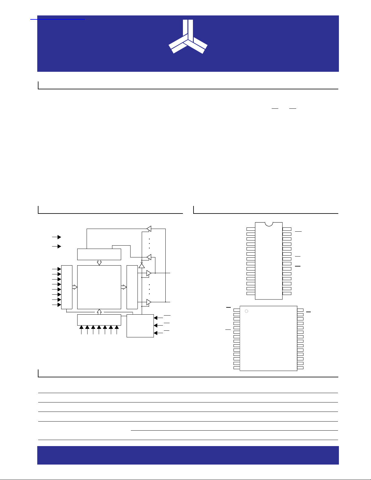
LOGIC BLOCK DIAGRAM
Vcc
GND
INPUT BUFFER
A0
A1
A2
A3
A4
A5
A6
A14
ROW DECODER
256×128×8
ARRAY
(262,144)
COLUMN DECODER
A8A
A9A10A11A12A
7
SELECTION GUIDE
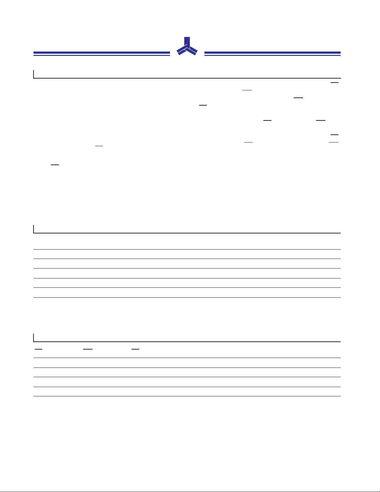
PIN ARRANGEME NT
DIP, SOJ, SOIC
I/O7
SENSE AMP
CONTROL
CIRCUIT
13
WE
OE
CE
I/O0
TSOP 8×13.4
A14
A12
A7
A6
A5
A4
A3
A2
A1
A0
I/O0
I/O1
I/O2
GND
OE A10
A11
A9
A8
A13
WE
Vcc
A14
A12
A7
A6
A5
A4
A3 A2
1
2
3
4
5
6
7
8
9
AS7C256
10
11
12
13
14
22
23
24
25
26
27
28
AS7C256
1
2
3
4
5
6
7
Vcc
28
WE
27
26
A13
25
A8
24
A9
23
A11
OE
22
A10
21
20
CE
19
I/O7
18
I/O6
17
I/O5
16
I/O4
15
I/O3
21
CE
20
I/O7
19
I/O6
18
I/O5
17
I/O4
16
I/O3
15
14
GND
13
I/O2
12
I/O1
11
I/O0
10
A0
9
8
AS7C256-02AS7C256-01
A1
7C256-10 7C256-12 7C256-15 7C256-20 7C256-25 7C256-35 Unit
Maximum Address Access Time 10 12 15 20 25 35 ns
Maximum Output Enable Access Time 334568ns
Maximum Operating Current 120 115 110 100 90 80 mA
Maximum CMOS Standby Current
2.0 2.0 2.0 2.0 2.0 2.0 mA
L 0.5 0.5 0.5 0.5 0.5 0.5 mA
ALLIANCE SEMICONDUCTOR
Page 2
AS7C256
AS7C256L
FUNCTIONAL DESCRIPTION
The AS7C256 is a high performance CMOS 262,144-bit
Static Random Access Memory (SRAM) organized as
32,768 words × 8 bits. It is designed for memory applications where fast data access, low power, and simple interfacing are desired.
Equal address access and cycle times (t
, tRC, tWC) of
AA
10/12/15/20/25/35 ns with output enable access times (t
of 3/3/4/5/6/8 ns are ideal for high performance applications. A chip enable (CE
) input permits easy memory
expansion with mult iple-bank memory organizations.
When CE
is HIGH the device enters standby mode. The
standard AS7C256 is guaranteed not to exceed 11 mW
A write cycle is accomplishe d by asserti n g chip enable (CE
and write enable (WE
) LOW. Data on the input pins
I/O0-I/O7 is writt en on the r ising edge of WE
(write cycle 2). To avoid bus contention, external
or CE
devices should drive I/O pins only after outputs have been
disabled with output enable (OE
)
OE
A read cycle is accompl ished by assert ing chip enable (CE
and output enable (OE
) LOW, with write enable (WE)
) or write enable (WE).
HIGH. The chip drives I/O pins with the data word referenced by the input address. When chip enable or output
enable is HIGH, or wri te enable is LOW, output drivers stay
in high-impedance mode.
(write cycle 1)
power consumption in standby mode; the L version is guaranteed not to exceed 2.75 mW, and typically requires only
500 µW. The L version also offers 2.0V data retention, with
maximum power consumption in this mode of 300 µW.
All chip inputs and outputs are TTL-compa tible, and operation is from a single 5V supply. The AS7C256 is packaged
in all high volume industry standard packages.
ABSOLUTE MAXIMUM RATINGS
Parameter Symbol Min Max Unit
Voltage on Any Pin Relative to G N D V
Power Dissipation P
Storage Temperature (Plastic) T
Temperatur e Under Bias T
DC Output Current I
NOTE: Stresses greater than those listed under Absolute Maximum Ratings may cause permanent damage to the device. This is a stress
rating only and functional operatio n of the device at these or any other conditions outside those indicated in the operationa l sections of
this specification is not implied. Exposure to absolute maximum rating conditions for extended periods may affect reliability.
.
t
D
stg
bias
out
–0.5 +7.0 V
– 1.0 W
–55 +150
–10 +85
–20mA
o
C
o
C
)
)
TRUT H TABLE
CE
HXXHigh Z Standby (I
L H H High Z Output Disable
LHLD
LLXD
Key: X = Don’t Care, L = LOW, H = HIGH
WE OE Data Mode
out
in
Read
Write
SB
, I
)
SB1
2
Page 3
AS7C256
AS7C256L
RECOMMEND ED OPER ATING C ONDITI ONS (Ta = 0°C to +70°C)
Parameter Symbol Min Typ Max Unit
Supply Voltage
Input Voltage
min = –3.0V for pulse width less than tRC/2.
*V
IL
DC OPERATING CHARACTERISTICS
Parameter Symbol Test Conditions
Input Leakage
Current
Output Leakage
Current
Operating Power
Supply Current
Standby
Power Supply
Current
Output Voltage
|ILI|
|ILO|
I
CC
I
SB
I
SB1
V
V
VCC = Max,
V
= GND to V
in
CE = VIH, VCC = Max,
V
= GND to V
out
CE = VIL, f = f
I
= 0 mA
out
CE = VIH, f = f
CE > VCC–0.2V, f = 0,
V
≤ 0.2V or
in
V
≥ V
CC
–0.2V
in
IOL = 8 mA, VCC = Min – 0.4 – 0.4 – 0.4 – 0.4 – 0.4 – 0.4 V
OL
IOH = –4 mA, VCC = Min 2.4 – 2.4 – 2.4 – 2.4 – 2.4 – 2.4 – V
OH
CC
max,
max
1
CC
V
CC
4.5 5.0 5.5 V
GND 0.0 0.0 0.0 V
V
IH
V
IL
2.2 – VCC+1 V
–0.5* – 0.8 V
(VCC = 5V±10% , GND = 0V, Ta = 0°C to +70°C)
-10 -12 -15 -20 -25 -35
UnitMin Max Min Max Min Max Min Max Min Max Min Max
–1–1–1–1–1–1µA
–1–1–1–1–1–1µA
–120–115–110–100– 90 – 80mA
L –115–110–105– 95 – 85 – 75mA
–45–40–30–30–25–25mA
L – 40 – 35 – 25 – 25 – 20 – 20 mA
– 2.0 – 2.0 – 2.0 – 2.0 – 2.0 – 2.0 mA
L – 0.5 – 0.5 – 0.5 – 0.5 – 0.5 – 0.5 mA
CAPACITANCE (f = 1 MHz, Ta = Room Temperature, VCC = 5V)
2
Parameter Symbol Signals Test Conditions Max Unit
Input Capacitance C
I/O Capacitance C
IN
I/O
A, CE, WE, OE Vin = 0V 5 pF
I/O Vin = V
= 0V 7 pF
out
3
Page 4

AS7C256
AAAA
AAAA
AAAA
AAAA
AAAA
AAAA
AAAA
AAAA
AAAA
AA
AA
AA
AAAA
AAAA
AAAA
AAAA
AAAA
AAAA
AAAA
AAAA
AAAA
AAAA
AAAA
AAAA
AAAA
AAAA
AAAA
AAAA
AAAA
AAAA
AAAA
AAAA
AAAA
AAAA
AAAA
AAAA
AAAA
AAAA
AAAA
AAAA
AAAA
AAAA
AAAA
AAAA
AAAA
AAAA
AAAA
AAAA
AAAA
AAAA
AAAA
AAAA
AAAA
AAAA
AAAA
AAAA
AAAA
AAAA
AAAA
AAAA
AAAA
AAAA
AAAA
AAAA
AAAA
AAAA
AAAA
AAAA
AAAA
AAAA
AAAA
AAAA
AAAA
AAAA
AAAA
AAAA
AAAA
AAAA
AAAA
AAAA
AAAA
AA
AA
AA
AA
AAAA
AAAA
AAAA
AAAA
AAAA
AAAA
AAAA
AAAA
AAAA
AAAA
AAAA
AAAA
AAAA
AAAA
AAAA
AAAA
AAAA
AAAA
AAAA
AAAA
A
A
A
A
AS7C256L
READ CYCLE (VCC = 5V±10%, GND = 0V, Ta = 0°C to +70°C)
3, 9
-10 -12 -15 -20 -25 -35
Parameter Symbol
Read Cycle Time t
Address Access Time t
Chip Enable (CE
Output Enable (OE
) Access Time t
) Access Time t
Output Hold from Address Change t
LOW to Output in Low Z t
CE
HIGH to Output in High Z t
CE
LOW to Output in Low Z t
OE
HIGH to Output in High Z t
OE
Power Up Time t
Power Down Time t
RC
AA
ACE
OE
OH
CLZ
CHZ
OLZ
OHZ
PU
PD
TIMING WAVEFORM OF READ CYCLE 1 (Address Controlled)
10 – 12 – 15 – 20 – 25 – 35 – ns
– 10 – 12 – 15 – 20 – 25 – 35 ns 3
– 10 – 12 – 15 – 20 – 25 – 35 ns 3
–3–3–4–5–6–8ns
2–3–3–3–3–3–ns 5
3–3–3–3–3–3–ns4, 5
–3–3–4–5–6–8ns4, 5
0–0–0–0–0–0–ns4, 5
–3–3–4–5–6–8ns4, 5
0–0–0–0–0–0–ns4, 5
– 10 – 12 – 15 – 20 – 25 – 35 ns 4, 5
3, 6, 7, 9
t
RC
Unit NotesMin Max Min Max Min Max Min Max Min Max Min Max
Address
t
AA
D
out
t
RC
3, 6, 8, 9
1
TIMING WAVEFORM OF READ CYCLE 2 (CE Controlled)
Data Valid
t
OH
CE
t
OE
OE
D
out
Supply
Current
t
t
CLZ
PU
t
ACE
t
OLZ
Data Valid
50% 50%
t
OHZ
t
CHZ
t
PD
I
CC
I
SB
AS7C256-04
4
Page 5

AS7C256
AAAA
AAAA
AAAA
AAAA
AA
AA
AA
AA
t
AW
AAAA
AAAA
AAAA
AAAA
AAAA
AAAA
AAAA
AAAA
AAAA
AAAA
AAAA
AAAA
AAAA
AAAA
AAAA
AAAA
AAAA
AAAA
AAAA
AAAA
AAAA
AAAA
AAAA
AAAA
AAAA
AAAA
AAAA
AAAA
AAAA
AAAA
AAAA
AAAA
AAAA
AAAA
AAAA
AAAA
AAAA
AAAA
AAAA
AAAA
AAAA
AAAA
AAAA
AAAA
AAAA
AAAA
AAAA
AAAA
AAAA
AAAA
AAAA
AAAA
AA
AA
AA
AA
AAAA
AAAA
AAAA
AAAA
AAAA
AAAA
AAAA
AAAA
AAAA
AAAA
AAAA
AAAA
AAAA
AAAA
AAAA
AAAA
AAAA
AAAA
AAAA
AAAA
AAAA
AAAA
AAAA
AAAA
AAAA
AAAA
AAAA
AAAA
AAA
AAA
AAA
AAA
Address
CE
WE
D
in
D
out
Data Valid
t
CW
t
WP
t
DW
t
DH
t
AH
t
WZ
t
WC
AAAA
AAAA
AAAA
AAAA
AAAA
AAAA
AAAA
AAAA
AAA
AAA
AAA
AAA
t
AS
AS7C256-06
AS7C256L
WRITE CYC LE (VCC = 5V±10% , GND = 0V, Ta = 0°C to +70°C)
11
-10 -12 -15 -20 -25 -35
Parameter Symbol
Write Cycle Time t
Chip Enable to Write En d t
Address Setup to Write End t
Address Setup Time t
Write Pulse Width t
Address Hold From End of Write t
Data Valid to Write End t
Data Hold Time t
Write Enable to Output in High Z t
Output Active from Write End t
WC
CW
AW
AS
WP
AH
DW
DH
WZ
OW
TIMING WAVEFOR M OF WRITE CYCLE 1 (WE Controlled)
10–12–15–20–20–30– ns
9 –10–12–12–15–20– ns
9 –10–12–12–15–20– ns
0–0–0–0–0–0–ns
7–8–9–12–15–17– ns
0–0–0–0–0–0–ns
6–6–8–10–10–15– ns
0–0–0–0–0–0–ns4, 5
–5–5–5–5–5–5ns4, 5
3–3–3–3–3–3–ns4, 5
10, 11
t
WC
t
AW
t
AH
Unit NotesMin Max Min Max Min Max M in Max Min Max Min Max
Address
t
WP
WE
t
AS
D
in
t
WZ
D
out
10, 11
TIMING WAVEFOR M OF WRITE CYCLE 2 (CE Controlled)
5
t
DW
Data Valid
t
OW
t
DH
AS7C256-05
Page 6

AS7C256
AAAA
AAAA
AAAA
AAAA
AAAA
AAAA
AAAA
AAAA
AAAA
AAAA
AAAA
AAAA
AAAA
AAAA
AAAA
AAAA
AAAA
AAAA
AAA
AAA
AAA
AAAA
AAAA
AAAA
AAAA
AAAA
AAAA
AAAA
AAAA
AAAA
AAAA
AAAA
AAAA
AAAA
AAAA
AAAA
AAAA
AAAA
AAAA
AAA
AAA
AAA
AS7C256L
DATA RETENTION CHARACTERISTICS (L Version Only)
Parameter Symbol Test Conditions Min Max Unit
V
for Data Retenti o n V
CC
Data Retention Current I
Chip Enable to Data Retention Time t
Operation Recovery Time t
Input Leakage Current
DATA RETENTION WAVEFORM
V
CC
CE
4.5V 4.5V
V
IH
AC TEST CONDITIONS
– Output load: see Figure B,
except for t
– Input pulse level: GND to 3.0V. See Figure A.
– Input rise and fall times: 5 ns. See Figure A.
– Input and output timing reference levels: 1.5V.
CLZ
and t
see Figure C.
CHZ
DR
CCDR
CDR
R
VCC = 2.0V
≥ V
CE
≥ V
V
in
V
CC
CC
≤ 0.2V
in
–0.2V
–0.2V or
2.0 – V
– 150 µA
0–ns
t
RC
–ns
| ILI | –1µA
(L Version Only)
Data retention mode
V
≥ 2.0V
DR
V
IH
168Ω
t
R
+1.728V
+5V
AS7C256-07
t
CDR
V
DR
Thevenin Equivalent:
D
out
+5V
480
GND
Ω
D
out
255Ω
Figure C: Output Load for t
+3.0V
GND
90%
10%
90%
10%
Figure A: Input Waveform
D
out
255Ω 30 pF*
Figure B: Output Load
AS7C256-08 AS7C256-09 AS7C256-10
NOTES
1. During VCC power-up, a pull-up resistor to VCC on CE is requir ed to me et ISB specification.
2. This parameter is sampl ed an d not 100% tested.
3. For test conditions, see AC Test Conditio ns, Figures A, B, C.
4. t
CLZ
and t
are specified with CL = 5pF as in Figure C. Transition is measured ±500mV from steady-state voltage.
CHZ
5. This parame ter is guarante e d but not teste d.
6. WE
is HIGH for read cycle.
7. CE
and OE are LOW for read cycl e.
8. Address valid prior to or coincident with CE
transition LOW.
9. All read cycle timings are referenced from the last valid address to the first transitioning address.
10. CE
or WE must be HIGH during address transitions.
11. All write cycle timings are referenced from the last valid address to the first transitioning address.
6
480
5 pF*
GND
Ω
*including scope
and jig capacitance
, t
CLZ
CHZ
Page 7

TYP I CAL DC AN D AC CHARAC TERIS TICS
Output voltage (V)
0.0 3.75
5.0
2.51.25
0
20
60
80
40
100
120
140
Output source current (mA)
Output source current I
OH
Output voltage (V)
0.0 3.75
5.0
2.51.25
Output si nk current (mA )
Output sink current I
OL
vs. output voltage V
OL
vs. output voltage V
OH
0
20
60
80
40
100
120
140
VCC = 5.0V
Ta = 25°C
VCC = 5.0V
Ta = 25°C
Capacitance (pF)
0 750
1000
500250
0
5
15
20
10
25
30
35
Change in t
AA
(ns)
Typical access time change ∆t
AA
vs. output capac itive loading
VCC = 4.5V
AS7C256
AS7C256L
Normalized supply current ICC, I
vs. supply voltage V
1.4
1.2
I
SB
1.0
, I
CC
0.8
CC
0.6
I
Normalized I
0.4
SB
0.2
0.0
4.0 5.5
5.04.5
Supply voltage (V)
Normalized access time t
vs. supply voltage V
1.5
1.4
1.3
1.2
1.1
CC
CC
AA
6.0
SB
Normalized supply current ICC, I
vs. ambient temperature T
1.4
1.2
I
SB
1.0
, I
CC
0.8
CC
0.6
0.4
Normalized I
0.2
I
SB
0.0
–55 80
35–10
Ambient temperature (°C)
Normaliz e d acc ess time t
vs. ambient tempe rat ure T
1.5
1.4
VCC = 5.0VTa = 25°C
1.3
1.2
1.1
AA
a
a
125
SB
Normalized supply current I
vs. ambient tempe rat ure T
625
(log scal e)
SB1
25
V
= 5.0V
CC
5
1
0.2
0.04
Normalized I
-55 80
35-10
Ambient temperature (°C)
Normalized supply current I
vs. cycle frequency 1/tRC, 1/t
1.4
1.2
VCC = 5.0V
CC
1.0
Ta = 25°C
0.8
0.6
SB1
a
CC
WC
125
1.0
Normalized access time
0.9
0.8
4.0 5.5
5.04.5
Supply voltage (V)
1.0
Normalized access time
0.9
0.8
6.0
–55 80
Ambient temperature (°C)
Normalized I
0.4
0.2
0.0
35–10
125
075
5025
100
Cycle frequency (MHz)
7
AS7C256-11
Page 8

AS7C256
AS7C256L
ORDERING CODES
Package / Access Time 10 ns 12 ns 15 ns 20 ns 25 ns 35 ns
Plastic DIP, 300 mil AS7C256-10PC
Plastic SOJ, 300 mil AS7C256-10JC
Plastic SOIC, 330 mil AS7C256-10SC
TSOP 8×13.4 AS7C256-10TC
AS7C256L-10PC
AS7C256L-10JC
AS7C256L-10SC
AS7C256L-10TC
AS7C256-12PC
AS7C256L-12PC
AS7C256-12JC
AS7C256L-12JC
AS7C256-12SC
AS7C256L-12SC
AS7C256-12TC
AS7C256L-12TC
AS7C256-15PC
AS7C256L-15PC
AS7C256-15JC
AS7C256L-15JC
AS7C256-15SC
AS7C256L-15SC
AS7C256-15TC
AS7C256L-15TC
AS7C256-20PC
AS7C256L-20PC
AS7C256-20JC
AS7C256L-20JC
AS7C256-20SC
AS7C256L-20SC
AS7C256-20TC
AS7C256L-20TC
AS7C256-25PC
AS7C256L-25PC
AS7C256-25JC
AS7C256L-25JC
AS7C256-25SC
AS7C256L-25SC
AS7C256-25TC
AS7C256L-25TC
AS7C256-35PC
AS7C256L-35PC
AS7C256-35JC
AS7C256L-35JC
AS7C256-35SC
AS7C256L-35SC
AS7C256-35TC
AS7C256L-35TC
PART NUMBERING SYSTEM
AS7C 256 X –XX X C
SRAM Prefix Device Number Blank = Standard Power
L = Low Power
Access Time Package: P = PDIP 300 mil
J = SOJ 3 00 mil
S = SOIC 330 mil
T = TSOP 8×14
Commercial Temperature Range,
0°C to 70 °C
REPRESENT AT IVE S, DISTRIB UT OR S, AND SA LES OFF ICE S
DOMESTIC REPS
ALABAMA
Concord Component
(205) 772-8883
ARIZONA
Competitive Technology
(602) 265-9224
ARKANSAS
Southern States Marketing
(214) 238-7500
CALIFORNIA
North:
Brooks Technical
(415) 960-3880
LA Area:
Competitive Tech.
(714) 450-0170
San Diego:
ATS
(619) 634-1488
COLORADO
Technology Sales
(303) 792-8835
CONNECTICUT
Kitchen & Kutchin Inc.
(203) 239-0212
DELAWARE
Vantage Sales
(609) 424-6777
FLORIDA
Micro-Electronic Comp.
Deerfield Beach
(305) 426-8944
Tampa
(813) 393-5011
GEORGIA
Concord Component
(404) 416-9597
HAWAII
Brooks Technical
(415) 960-3880
IDAHO
ES/Chase
(503) 684-8500
ILLINOIS
North:
El-Mech
(312) 794-9100
South:
CenTech
(314) 291-4230
Alliance Semiconductor reserves the right to make changes in this data sheet at any time to improve design and supply the best product possible. Alliance Semiconductor cannot
assume responsibility for circuits shown or represent that they are free from patent infringement. Alliance products are not authorized for use as critical components in life
support devices or systems without the express written approval of the president of Alliance. The Alliance logo is a trademark of Alliance Semiconductor Corporation. All other
trademarks are property of their respective holders.
INDIANA
CC Electro Sales
(317) 921-5000
KANSAS
CenTech
(816) 358-8100
KENTUCKY
CC Electro Sales
(317) 921-5000
LOUISIANA
Southern States Marketing
North:
(214) 238-7500
South:
(713) 868-5180
MAINE
Kitchen & Kutchin Inc.
(617) 229-2660
MARYLAND
Ches apeake Technology
(301) 236-0530
MASSACHUSETTS
Kitchen & Kutchin Inc.
(617) 229-2660
MICHIGAN
Enco Group
(810) 338-8600
MINNESOTA
D. A. Case Associates
(612) 831-6777
MISSOURI
East: CenTech
(314) 291-4230
West:
CenTech
(816) 358-8100
MISSISSIPPI
Conc ord Component
(205) 772-8883
MONTANA
ES/Chase
(503) 684-8500
NEBRASKA
CenTech
(816) 358-8100
NEVADA
North:
Brooks Technical
(415) 960-3880
South:
Competitive Tech.
(602) 265-9224
NEW HAMPSHIRE
Kitchen & Kutchin Inc.
(617) 229-2660
NEW JERSEY
North:
ERA Associates
(800) 645-5500
South:
Vantage Sales
(609) 424-6777
NEW MEXICO
Competitive Techno logy
(602) 265-9224
NEW YORK
NYC:
ERA Associates
(516) 543-0510
Upstate:
Tri-Tech
Rochester
(716) 385-6500
Birmingham
(607) 722-3580
Fishkill
(914) 897-5611
NORTH CAROLINA
Concord Component
(919) 846-3441
NORTH DAKOTA
D. A. Case Associates
(612) 831-6777
OHIO
Midwest Marketing Assoc.
Lyndhurst:
(216) 381-8575
Dayton:
(513) 433-2511
OKLAHOMA
Southern States Marketing
(214) 238-7500
OREGON
ES/Chase
(503) 684-8500
PENNSYLVANIA
East:
Vantage Sales
(609) 424-6777
West:
Midwe st Marketing
(216) 381-8575
RHODE ISLAND
Kitchen & Kutchin Inc.
(617) 229-2660
SOUTH CAROLINA
Concord Component
(919) 846-3441
SOUTH DAKOTA
D. A. Case Associates
(612) 831-6777
TENNESSEE
Concord Component
(205) 772-8883
TEXAS
Southern States Marketing
Austin:
(512) 835-5822
Dallas:
(214) 238-7500
Houston:
(713) 868-5180
UTAH
Charles Fields & Assoc.
(801) 299-8228
VERMONT
Kitchen & Kutchin Inc.
(617) 229-2660
VIRGINIA
Chesapeake Technology
(301) 236-0530
WASHINGTON
ES/Chase
(206) 823-9535
WEST VIRGINIA
Chesapeake Technology
(301) 236-0530
WISCONSIN
D. A. Case Associates
(612) 831-6777
WYOMING
Technology Sales
(303) 777-9726
INTERNATIONAL
AUSTRALIA
NJS Technology Pty Ltd.
Mulgrave, Victoria
+61-3-562-1244
R&D Electronics
Dingley, Victori a
+61-3-558-0444
CANADA
Tech Trek Ltd.
Mississauga:
(905) 238-0366
Montreal:
(514) 337-7540
Ottawa:
(613) 599-8787
Vancouver:
(604) 276-8735
Calgary:
(403) 291-6866
EUROPE
Britcomp Sales
Surrey, England
+44-1932 347077
+44-1932 346256
Munich, Germany
+49-894488 496
Athismons, France
+33-1-69387678
HONG KONG
Eastele Technology
+85-2-798-8860
INDIA
Priya Electronics, Inc.
San Jose, CA USA
(408) 954-1866
ISRAEL
Eldis Technology
+972-9-562-666
JAPAN
Actes Engineering
Tokyo
+81-3-3769-3029
Rohm Co. Ltd.
Kyoto
+81-75-311-2121
KOREA
FM Korea
+822-575-9720
Woo Young Tech
+822-369-7099
MALAYSIA,
SINGAPORE
Technology Distr. Pte Ltd.
+65-299-7811
PUERTO RICO
Micro-Electronic Comp.
(809) 746-9897
TAIWAN
Asian Specific Tech.
+886-2-521-2363
Puteam International
+886-2-729-0373
DISTRIBUTORS
All-American
Locations Nationwide
Headquarters
Axis Components
Sunnyvale, CA
(408) 522-9595
Axis Components
Irvine, CA
(714) 459-5510
Future Electronics
Locations Worldwide
Headquarters
Interface Electronics
Hopkinton, MA
(800) 632-7792
(508) 435-0100
:
(305 ) 621-8282
:
(514 ) 594-7710
SALES OFFICES
HEADQUARTERS
Alliance Semiconductor
San Jose, CA
(408) 383-4900
NORTHEAST AREA
Alliance Semiconductor
Boston, MA
(617) 239-8127
TECHNICAL CENTER
TAIWAN
Alliance Semiconductor
+886-2-723-9944
ALLIANCE SEMICONDUCTOR
3099 North First Street San Jose, CA 95134
(408) 383-4900 Fax (408) 383-4999
Printed in U.S.A. Copyright © 1995 All rights reserved. May 1996
 Loading...