

Page 1

May 2002
5V/3.3V 128KX8 CMOS SRAM (Evolutionary Pinout)
Features
• AS7C1024A (5V version)
• AS7C31024A (3.3V version)
• Industrial and commercial temperatures
• Organization: 131,072 words x 8 bits
•High speed
- 10/12/15/20 ns address access time
- 5, 6, 7, 8 ns output enable access time
• Low power consumption: ACTIVE
- 853 mW (AS7C1024A) / max @ 10 ns
- 522 mW (AS7C31024A) / max @ 10 ns
• Low power consumption: STANDBY
- 55 mW (AS7C1024A) / max CMOS
- 36 mW (AS7C31024A) / max CMOS
®
• Latest 6T 0.25u CMOS technology
• Easy memory expansion with CE1
• TTL/LVTTL-compatible, three-state I/O
• 32-pin JEDEC standard packages
- 300 mil SOJ
- 400 mil SOJ
-8 × 20mm TSOP 1
- 8 x 13.4mm sTSOP 1
• ESD protection ≥ 2000 volts
• Latch-up current ≥ 200 mA
Pin arrangement
32-pin SOJ (300 mil)
32-pin SOJ (400 mil)
AS7C1024A
AS7C31024A
, CE2, OE inputs
Logic block diagram
V
CC
GND
Input buffer
A0
A1
A2
A3
A4
A5
A6
A7
A8
Row decoder
512×256×8
(1,048,576)
Column decoder
A9
A10
Array
A11
A12
1
NC
2
A16
3
A14
4
A12
5
A7
6
A6
7
A5
8
A4
9
A3
10
A2
11
A1
A0
I/O0
I/O1
I/O2
I/O7
Sense amp
I/O0
Control
circuit
A13
A14
A15
A16
WE
OE
CE1
CE2
GND
32-pin (8 x 20mm) TSOP I
32-pin (8 x 13.4mm) sTSOP1
A11 OE
1
2
A9
3
A8
4
A13
5
WE
6
CE2
7
A15
8
V
CC
9
NC
10
A16
11
A14
12
A12
13
A7
14
A6
15
A5
16
A4 A3
12
13
14
15
16
AS7C1024A
AS7C1024A
V
32
A15
31
CE2
30
29
WE
28
A13
27
A8
26
A9
A11
25
24
OE
23
A10
22
CE1
AS7C31024A
21
I/O7
20
I/O6
19
I/O5
18
I/O4
17
I/O3
AS7C31024A
CC
32
A10
31
CE1
30
I/O7
29
28
I/O6
27
I/O5
26
I/O4
25
I/O3
24
GND
23
I/O2
22
I/O1
21
I/O0
20
A0
19
A1
18
A2
17
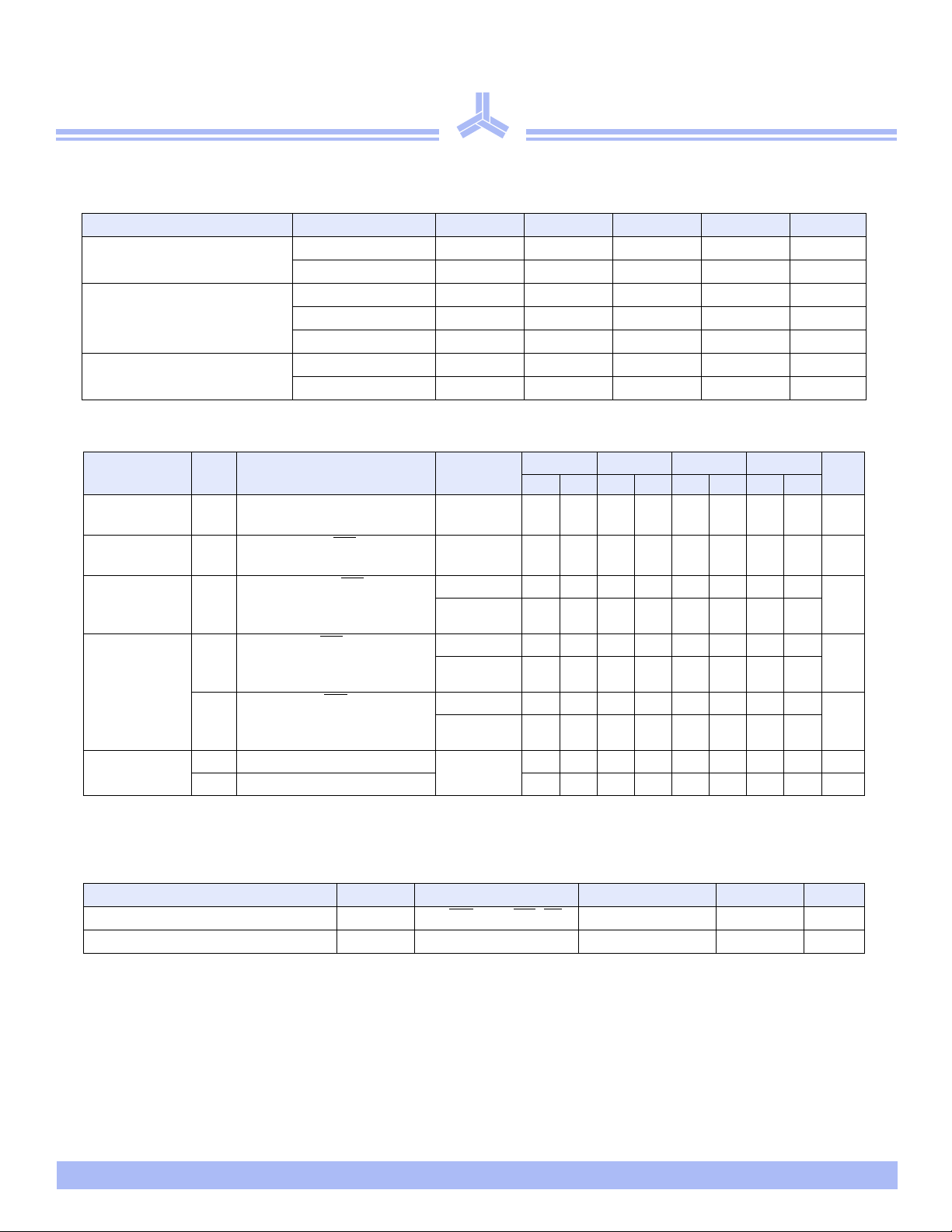
Selection guide
-10
Maximum address access time 10 12 15 20 ns
Maximum output enable access time 5 6 7 8 ns
Maximum
operating current
Maximum CMOS
standby current
AS7C1024A 155 150 145 140 mA
AS7C31024A 145 140 135 130 mA
AS7C1024A 10 10 10 10 mA
AS7C31024A 5 5 5 5 mA
-12 -15 -20 Unit
9/26/02; 0.9.9
Alliance Semiconductor
P. 1 of 9
Copyright © Alliance Semiconductor. All rights reserved.
Page 2

AS7C1024A
AS7C31024A
®
Functional description
The AS7C1024A and AS7C31024A are high performance CMOS 1,048,576-bit Static Random Access Memory (SRAM) devices organized as
131,072 words x 8 bits. It is designed for memory applications where fast data access, low power, and simple interfacing are desired.
Equal address access and cycle times (tAA, tRC, tWC) of 10/12/15/20 ns with output enable access times (tOE) of 5, 6, 7, 8 ns are ideal for high
performance applications. Active high and low chip enables (CE1, CE2) permit easy memory expansion with multiple-bank systems.
When CE1 is high or CE2 is low the devices enter standby mode. If inputs are still toggling, the device will consume ISB power. If the bus is
static, then full standby pow er is reached (I
conditions. All devices in this family will retain data when VCC is reduced as low as 2.0V.
A write cycle is accomplished by asserting write enable (WE) and both chip enables (CE1, CE2). Data on the input pins I/O0-I/O7 is wr itten
on the rising edge of WE
should drive I/O pins only after outputs have been disabled with output enable (OE) or write enable (WE).
A read cycle is accomplished by asserting output enable (OE) and both chip enables (CE1, CE2), with write enable (WE) high. The chips drive
I/O pins with the data word referenced by the input address. When either chip enable is inactive, output enable is inactive, or write enable is
active, output drivers stay in high-impedance mode.
(write cycle 1) or the active-to-inactive edge of CE1 or CE2 (write cycle 2). To avoid bus contention, external devices
). For example, the AS7C31024A is guaranteed not to exceed 36mW under nominal full standby
SB1
Absolute maximum ratings
Parameter Symbol Min Max Unit
Voltage on V
relative to GND
CC
AS7C1024A V
AS7C31024A V
Voltage on any pin relative to GND Both V
Power dissipation Both P
Storage temperature (plastic) Both T
Ambient temperature with V
applied Both T
CC
DC current into outputs (low) Both I
Note: Stresses greater than those listed under Absolute Maximum Ratings may cause perma nent damage to the device. This is a stress rating only and functional operation of the device at these or any other conditions outside those indicated in the operational sections of this specification is not implied. Exposure to absolute
maximum rating conditions for extended periods may affect reliability.
t1
t1
t2
D
stg
bias
OUT
–0.50 +7.0 V
-0.50 +5.0 V
–0.50 VCC +0.50 V
–1.0W
–65 +150
–55 +125
C
°
C
°
–20mA
Truth table
CE1
HXXX High Z Standby (I
XLXX High Z Standby (I
L H H H High Z Output disable (I
LHHL D
LHLX D
Key: X = Don’t Care, L = Low, H = High
CE2
WE OE
Data Mode
OUT
IN
Read (ICC)
Write (
SB
SB
ICC
, I
, I
SB1
SB1
)
CC
)
)
)
9/26/02; 0.9.9
Alliance Semiconductor
P. 2 of 9
Page 3
Recommended operating conditions
Parameter Device Symbol Min Nominal Max Unit
Supply voltag e
Input voltage
Ambient operating temperature
VILmin. = –3.0V for pulse width less than t
1
AS7C1024A V
AS7C31024A V
ASAS7C1024A V
AS7C31024A V
commercial T
industrial T
.
RC/2
CC
CC
IH
IH
1
V
IL
A
A
DC operating characteristics (over the operating range)
Parameter Sym Test conditions Device
Input lea k age
current
Output leakage
current
Operating
pow er suppl y
current
Standby power
supply current
Output voltage
|I
|VCC = Max, VIN = GND to V
LI
V
= Max, CE1 = VIH or
|
|I
LO
CC
CE2 = V
, V
= GND to V
IL
OUT
VCC = Max, CE1 = VIL,
CE2 = V
I
CC
IH
, f = f
Max
mA
VCC = Max, CE1 ≥ VIH and/or
≤
CE2
I
SB
VIL, VIN = VIH or VIL,
f = f
, I
Max
OUT
VCC = Max, CE1 ≥ VCC–0.2V
V
I
SB1
V
OL
V
OH
≤ GND + 0.2V or
IN
V
≥ VCC –0.2V, f = 0
IN
IOL = 8 mA, VCC = Min
IOH = –4 mA, VCC = Min 2.4 – 2.4 – 2.4 – 2.4 – V
, I
OUT
= 0mA
CC
Both –1–1–1–1µA
Both –1–1–1–1µA
CC
AS7C1024A – 155 – 150 – 145 – 140
= 0
AS7C31024A – 145 – 140 – 135 – 130
AS7C1024A – 30 – 25 – 20 – 20
AS7C31024A – 30 – 25 – 20 – 20
AS7C1024A – 10 – 10 – 10 – 10
AS7C31024A – 5 – 5 – 5 – 5
Both
AS7C1024A
AS7C31024A
®
4.5 5.0 5.5 V
3.0 3.3 3.6 V
2.2 – VCC + 0.5 V
2.0 – VCC + 0.5 V
–0.5 – 0.8 V
0–70°C
–40 – 85
-10 -12 -15 -20
Min Max Min Max Min Max Min Max
–0.4–0.4–0.4–0.4V
C
°
Unit
mA
mA
mA
Capacitance (f = 1 MHz, Ta = 25 °C, VCC = NOMINAL)
Parameter Symbol Signals Test conditions Max Unit
Input capacitance C
I/O capacitance C
9/26/02; 0.9.9
IN
I/O
Alliance Semiconductor
A, CE1, CE2, WE, OE VIN = 0V 5 pF
I/O VIN = V
2
= 0V 7 pF
OUT
P. 3 of 9
Page 4

AS7C1024A
AS7C31024A
®
Read cycle (over the operating range)
Parameter Symbol
Read cycle time t
Address access time t
Chip enable (CE1
) access time t
Chip enable (CE2) access time t
Output enable (OE
) access time t
Output hold from address change t
CE1
Low to output in low Z t
CE2 High to output in low Z t
CE1
Low to output in high Z t
CE2 Low to output in high Z t
OE
Low to output in low Z t
OE
High to output in high Z t
Power up time t
Power down time t
RC
AA
ACE1
ACE2
OE
OH
CLZ1
CLZ2
CHZ1
CHZ2
OLZ
OHZ
PU
PD
Key to switching waveforms
-10 -12 -15 -20
Unit NotesMin Max Min Max Min Max Min Max
10 – 12 – 15 – 20 – ns
– 10 – 12 – 15 – 20 ns 3
– 10 – 12 – 15 – 20 ns 3, 12
– 10 – 12 – 15 – 20 ns 3, 12
–5–6–7–8 ns
2–3–3–3– ns 5
0–0–0–0– ns4, 5, 12
0–0–0–0– ns4, 5, 12
–3–3–4–5 ns4, 5, 12
–3–3–4–5 ns4, 5, 12
0–0–0–0– ns 4, 5
–3–3–4–5 ns 4, 5
0–0–0–0– ns4, 5, 12
– 10 – 12 – 15 – 20 ns 4, 5, 12
Undefined / don’ t careFalling inputRising input
Read waveform 1 (address controlled)
Address
D
OUT
t
RC
t
AA
Read waveform 2 (CE1, CE2, and OE controlled)
t
CE1
CE2
OE
D
OUT
Current
supply
t
ACE1, tACE2
t
, t
CLZ1
t
PU
CLZ2
RC1
t
OE
t
OLZ
50% 50%
Data valid
Data valid
t
OH
t
OHZ
t
, t
CHZ1
CHZ2
t
PD
I
CC
I
SB
9/26/02; 0.9.9
Alliance Semiconductor
P. 4 of 9
Page 5

AS7C1024A
AS7C31024A
®
Write cycle (over the operating range)
Parameter Symbol
Write cycle time t
Chip enable (CE1
) to write end t
Chip enable (CE2) to write end t
Address setup to write end t
Address setup time t
Write pulse width t
Write recovery time t
Address hold from end of write t
Data valid to write end t
Data hold time t
Write enable to output in high Z t
Output active from write end t
Write waveform 1 (WE controlled)
Address
WE
t
AS
D
IN
D
OUT
WC
CW1
CW2
AW
AS
WP
WR
AH
DW
DH
WZ
OW
t
-10 -12 -15 -20
Unit NotesMin Max Min Max Min Max Min Max
10 – 12 – 15 – 20 – ns
8 – 10 – 12 – 12 – ns 12
8 – 10 – 12 – 12 – ns 12
8 – 9 – 10 – 12 – ns
0 – 0 – 0 – 0 – ns 12
7 – 8 – 9 – 12 – ns
0–0–0–0–ns
0–0–0–0–ns
5 – 6 – 8 – 10 – ns
0 – 0 – 0 – 0 – ns 4, 5
– 6 – 6 – 6 – 8 ns 4, 5
1 – 1 – 1 – 2 – ns 4, 5
t
WZ
WC
t
AW
t
WP
t
DW
Data valid
t
OW
t
t
t
WR
AH
DH
Write waveform 2 (CE1 and CE2 controlled)
t
AW
Address
t
CW1
t
WZ
Alliance Semiconductor
CE1
CE2
WE
D
IN
D
OUT
9/26/02; 0.9.9
t
AS
t
WC
, t
CW2
t
WP
t
DW
Data valid
t
t
AH
WR
t
DH
P. 5 of 9
Page 6

®
AC test conditions
– Output load: see Figure B or Figure C.
– Input pulse level: GND to 3.0V. See Figure A.
– Input rise and fall times: 2 ns. See Figure A.
– Input and output timing reference levels: 1.5V.
D
+3.0V
GND
90%
10%
2 ns
Figure A: Input pulse
90%
10%
OUT
Figure B: 5V Output load
255
+5V
480
Ω
Ω
C(14)
GND
D
D
OUT
OUT
Notes
1During VCC power-up, a pull-up resistor to VCC on CE1 is required to meet I
2 This parameter is sampled and not 100% tested.
3 For test conditions, see AC Test Conditions, Figures A, B, and C.
4t
and t
CLZ
5 This parameter is guaranteed, but not 100% tested.
6WE
is High for read cycle.
7CE1
8 Address valid prior to or coincident with CE1
9 All read cycle timings are referenced from the last valid address to the first transitioning address.
10 CE1
11 All write cycle timings are referenced from the last valid address to the first transitioning address.
12 CE1
13 C=30pF, except all high Z and low Z parameters, C=5pF.
14 2V data retention applies to commercial temperature operating range only.
are specified with CL = 5pF, as in Figure C. Transition is measured ±500mV from steady-state voltage.
CHZ
and OE are Low and CE2 is High for read cycle.
transition Low.
or WE must be High or CE2 Low during address transitions. Either CE1 or WE asserting high terminates a write cycle.
and CE2 have identical timing.
specification.
SB
Thevenin equivalent:
168
Ω
+1.728V (5V and 3.3V)
+3.3V
320
Ω
255
Ω
C(14)
GND
Figure C: 3.3V Output load
AS7C1024A
AS7C31024A
9/26/02; 0.9.9
Alliance Semiconductor
P. 6 of 9
Page 7

Typical DC and AC Characteristcs
AS7C1024A
AS7C31024A
®
Normalized supply current ICC, I
vs. supply voltage V
1.4
1.2
I
SB
1.0
, I
CC
0.8
CC
0.6
0.4
Normalized I
0.2
I
SB
0.0
MIN
NOMINAL
Supply voltage (V)
Normalized access time t
vs. supply voltage V
1.5
1.4
1.3
1.2
1.1
Ta = 25° C
1.0
Normalized access time
0.9
CC
CC
AA
SB
MAX
Normalized supply current ICC, I
vs. ambient temperature T
1.4
1.2
SB
1.0
, I
CC
0.8
0.6
0.4
Normalized I
0.2
0.0
–55 80
35–10
Ambient temperature (°C)
Normalized access time t
vs. ambient temperature T
1.5
1.4
1.3
VCC = VCC(NOMINAL)
1.2
1.1
1.0
Normalized access time
0.9
SB
a
I
CC
Normalized supply current I
vs. ambient temperature T
625
25
VCC = VCC(NOMINAL)
SB1
a
5
1
I
SB
125
0.2
0.04
Normalized ISB1 (log scale)
-55 80
35-10
125
Ambient temperature (°C)
AA
a
Normalized supply current I
vs. cycle frequency 1/tRC, 1/t
1.4
CC
WC
1.2
1.0
0.8
0.6
Normalized ICC
0.4
VCC = VCC(NOMINAL)
Ta = 25° C
0.2
0.8
140
120
100
80
60
MIN
NOMINAL
Supply voltage (V)
Output source current I
vs. output voltage V
VCC = VCC(NOMINAL)
MAX
OH
OH
0.8
–55 80
35–10
Ambient temperature (°C)
Output sink current I
vs. output voltage V
140
120
100
VCC = VCC(NOMINAL)
80
Ta = 25° C
60
OL
OL
125
0.0
075
Cycle frequency (MHz)
Typical access time change ∆t
vs. output capacitive loading
35
30
25
(ns)
AA
VCC = VCC(NOMINAL)
20
15
Ta = 25° C
CC
10
Change in t
5
0
Capacitance (pF)
40
20
Output source current (mA)
0
0 750
V
CC
Output voltage (V)
9/26/02; 0.9.9
40
Output sink current (mA)
20
0
00
V
Output voltage (V)
Alliance Semiconductor
5025
500250
100
AA
1000
P. 7 of 9
Page 8

Package dimensions
AS7C1024A
AS7C31024A
®
Pin 1
A2
32-pin SOJ 300
mil
D
e
Min Max Min Max
A - 0.145 - 0.145
32-pin SOJ 400
mil
A1 0.025 - 0.025 -
E2
E1
A2 0.086 0.105 0.086 0.115
B 0.026 0.032 0.026 0.032
B
c
E
A1
b
Seating
Plane
b 0.014 0.020 0.015 0.020
c 0.006 0.013 0.007 0.013
A
D 0.820 0.830 0.820 0.830
E 0.250 0.275 0.360 0.380
E1 0.292 0.305 0.395 0.405
E2 0.330 0.340 0.435 0.445
e 0.050 BSC 0.050 BSC
32-pin TSOP 8×20 mm
Min Max
b
e
A – 1.20
A1 0.05 0.15
α
A2 0.95 1.05
b 0.17 0.27
c
D
L
Hd
A1AA2
c 0.10 0.21
D 18.20 18.60
e 0.50 nominal
E 7.80 8.20
pin 1 pin 32
Hd 19.80 20.20
L 0.50 0.70
α
0° 5°
E
9/26/02; 0.9.9
pin 16 pin 17
Alliance Semiconductor
P. 8 of 9
Page 9

p
p
Ordering codes
Package \ Access
time
Plastic SOJ, 300 mil
Plastic SOJ, 400 mil
TSOP1 8×20 mm
sTSOP1
8 x 13.4mm
Volt/Temp
5V commercial
5V industrial
3.3V commercial
3.3V industrial
5V commercial
5V industrial
3.3V commercial
3.3V industrial
5V commercial
5V industrial
3.3V commercial
3.3V industrial
5V commercial
5V industrial
3.3V commercial
3.3V industrial
ASAS7C1024A
ASAS7C31024A
®
10 ns 12 ns 15 ns 20 ns
AS7C1024A-10TJC AS7C1024A-12TJC AS7C1024A-15TJC AS7C1024A-20TJC
AS7C1024A-10TJI AS7C1024A-12TJI AS7C1024A-15TJI AS7C1024A-20TJI
AS7C31024A-10TJC AS7C31024A-12TJC AS7C31024A-15TJC AS7C31024A-20TJC
AS7C31024A-10TJI AS7C31024A-12TJI AS7C31024A-15TJI AS7C31024A-20TJI
AS7C1024A-10JC AS7C1024A-12JC AS7C1024A-15JC AS7C1024A-20JC
AS7C1024A-10JI AS7C1024A-12JI AS7C1024A-15JI AS7C1024A-20JI
AS7C31024A-10JC AS7C31024A-12JC AS7C31024A-15JC AS7C31024A-20JC
AS7C31024A-10JI AS7C31024A-12JI AS7C31024A-15JI AS7C31024A-20JI
AS7C1024A-10TC AS7C1024A-12TC AS7C1024A-15TC AS7C1024A-20TC
AS7C1024A-10TI AS7C1024A-12TI AS7C1024A-15TI AS7C1024A-20TI
AS7C31024A-10TC AS7C31024A-12TC AS7C31024A-15TC AS7C31024A-20TC
AS7C31024A-10TI AS7C31024A-12TI AS7C31024A-15TI AS7C31024A-20TI
AS7C1024A-10STC AS7C1024A-12STC AS7C1024A-15STC AS7C1024A-20STC
AS7C1024A-10STI AS7C1024A-12STI AS7C1024A-15STI AS7C1024A-20STI
AS7C31024A-10STC AS7C31024A-12STC AS7C31024A-15STC AS7C31024A-20STC
AS7C31024A-10STI AS7C31024A-12STI AS7C31024A-15STI AS7C31024A-20STI
Part numbering system
AS7C X 1024A –XX X X
Package:T=TSOP1 8×20 mm
SRAM
prefix
Blank=5V CMOS
3=3.3V CMOS
Device
number
Access
time
ST=sTSOP1 8 x 13.4 mm
J=SOJ 400 mil
TJ=SOJ 300 mil
9/26/02; 0.9.9
© C op y rig ht Allianc e S em ico n du cto r C o rp or atio n. A ll rig ht s res erv ed . O u r th re e-p o int lo g o, o u r n ame an d I nte lliw a tt are trad em ark s o r re gi stere d tr ad emark s o f A llia nc e. All oth er b ra nd an d
rodu ct n ames m a y b e th e t rad emark s o f th eir resp ec tive co m p a nie s. A llia nc e re ser ve s the rig ht to make ch an g es to thi s do cu m e nt an d its p ro d u cts at a n y time w ith ou t n o tice . A llia n ce assu mes no
responsibility for any errors that may appear in this document. The data contained herein represents Alliance’s best data and/or estimates at the tim e of issuan ce. A lliance reserv es the right to
chang e o r c o rrec t th is da ta a t an y ti m e, w itho u t n otic e. I f the pr o du ct d esc rib ed h ere in is un de r d ev elo p m e nt, si gn ific an t ch an ge s to the se sp ec ific atio ns are po ssib le. The in fo rmatio n in th is
rodu ct d ata she et is in ten d ed to be ge ne ral d esc rip tiv e in fo rmation fo r p o ten tial c usto mers an d use rs, an d is n o t inte nd e d to o perate as, or provide, any guarantee or warrantee to any user or
customer. A l lian ce d o es n ot a ssu m e an y r esp o nsib ility or liab ility a risin g ou t o f th e ap p licat ion o r u se o f an y pr od u ct d esc ribe d h e rein , an d disc laim s an y ex pre ss o r implie d w a rr an ties r elate d to
the sale a nd /o r u se o f A llia nc e p ro du ct s inc lud in g lia b ility o r w a rr an ties r elate d to fitn e ss fo r a p ar ticu lar pu rp os e, merch an tab ility , or in frin ge m e n t of a ny in telle ctu al p ro pe rty rig h ts, ex ce pt a s
expre ss ag re ed to in A lli an ce’s Term s an d C o n ditio n s of S ale (w h ich ar e av aila ble fr om A llian ce ). A ll sale s of A llian ce pr od u cts ar e made ex clu siv ely ac co rd ing to A llia nc e’s T e rms and
Conditions of Sale. The purchase of products from Alliance does not convey a license under any patent rights, copyrights, mask works rights, trademarks, or any other in tellectual prop erty rights
of All ian ce o r third p ar ties. A lli an ce d o es n o t au tho riz e its p ro d uc ts fo r u se as critic al c ompo n en ts in lif e-s up p or ting sy stems w he re a m a lfu nc tio n o r f ailu re may rea so na bly b e ex p ect ed to re su lt
in signi fica nt in ju ry to th e u se r, an d the inc lu sion o f A llia nc e p ro du c ts in s uc h life -su p po rtin g sys tems im p lies th at th e man ufa ctu re r ass umes a ll risk of suc h u se an d a gr ee s to in d emnify A llia nc e
against all claims arisin g from such use.
Alliance Semiconductor
Temperature range
C = Commercial, 0°C to 70°C
I = Industrial, -40°C to 85°C
P. 9 of 9
 Loading...