

Datasheet AS5SS256K18DQ-9-XT, AS5SS256K18DQ-9-IT, AS5SS256K18DQ-8-XT, AS5SS256K18DQ-8-IT, AS5SS256K18DQ-10-XT Datasheet (AUSTN)
...Page 1
AS5SS256K18
Rev. 2.0 12/00
Austin Semiconductor, Inc. reserves the right to change products or specifications without notice.
1
SSRAM
AS5SS256K18
Austin Semiconductor, Inc.
FEA TURES
• Fast access times: 8, 10, and 15ns
• Fast clock speed: 113, 100, and 66 MHz
• Fast clock and OE\ access times
• Single +3.3V +0.3V/-0.165V power supply (VDD)
• SNOOZE MODE for reduced-power standby
• Common data inputs and data outputs
• Individual BYTE WRTIE control and GLOBAL WRITE
• Three chip enables for simple depth expansion and address
pipelining
• Clock-controlled and registered addresses, data I/Os and
control signals
• Interally self-timed WRITE cycle
• Burst control pin (interleaved or linear burst)
• Automatic power-down
• Low capacitive bus loading
• Operating Temperature Ranges:
- Military -55oC to +125oC
- Industrial -40oC to +85oC
OPTIONS MARKING
• Timing
7.5ns/8ns/113 MHz -8 *
8.5ns/10ns/100 MHz -9
10ns/15ns/66 MHz -1 0
• Packages
100-pin TQFP DQ No. 1001
• Operating Temperature Ranges:
- Military -55oC to +125oCIT
- Industrial -45oC to +85oCXT
*available as IT only.
256K x 18 SSRAM
Synchronous Burst SRAM,
Flow-Through
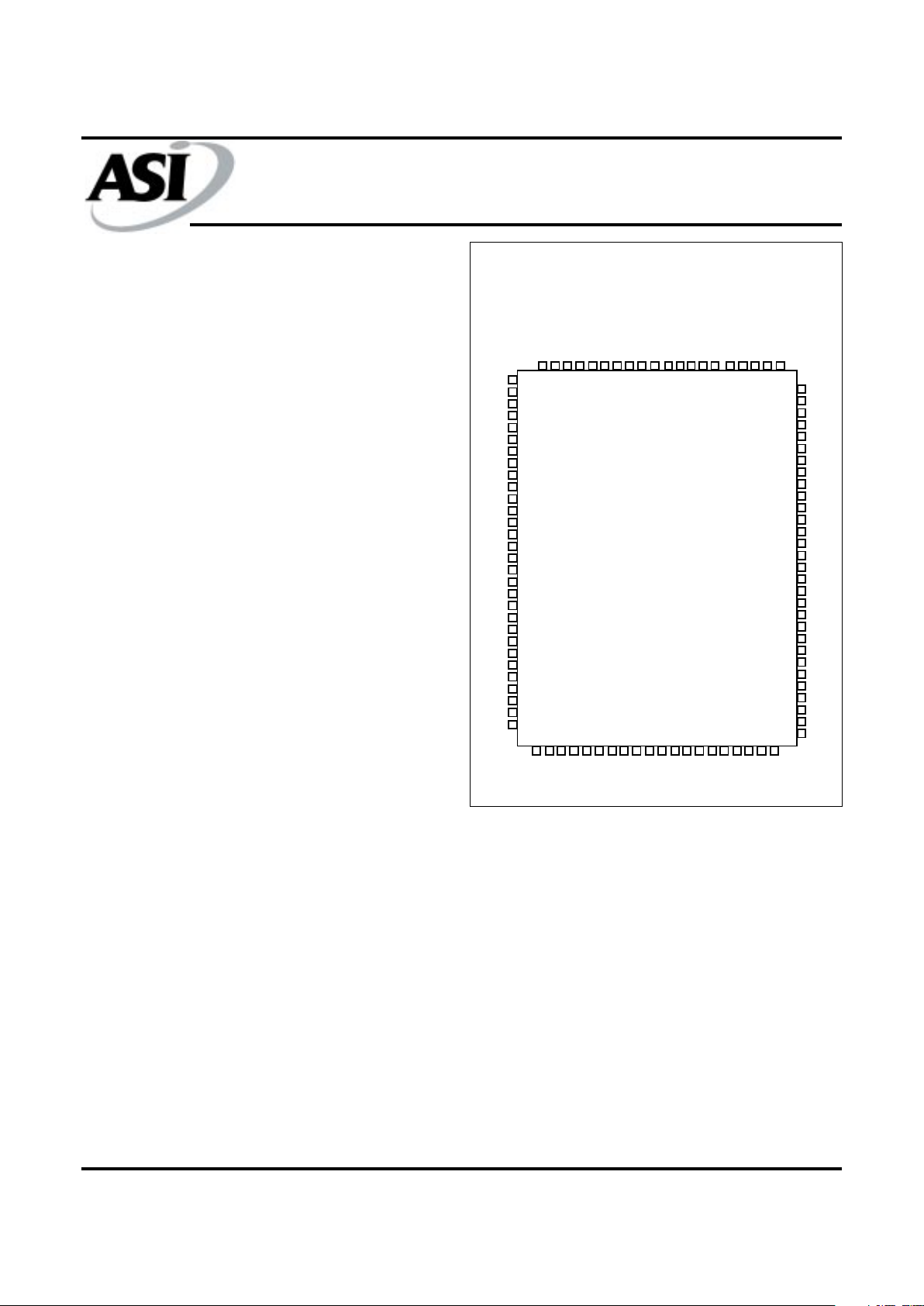
PIN ASSIGNMENT
(Top View)
100-pin TQFP
For more products and information
please visit our web site at
www.austinsemiconductor .com
SA
SA
CE\
CE2
NC
NC
bwB\
BWa\
CE2\
V
DD
V
SS
CLK
GW\
BWE\
OE\
ADSC\
ADSP\
ADV\
SA
SA
1
2
3
4
5
6
7
8
9
10
11
12
13
14
15
16
17
18
19
20
21
22
23
24
25
26
27
28
29
30
80
79
78
77
76
75
74
73
72
71
70
69
68
67
66
65
64
63
62
61
60
59
58
57
56
55
54
53
52
51
31 32 33 34 35 36 37 38 39 40 41 42 43 44 45 46 47 48 49 50
100 99 98 97 96 95 94 93 92 91 90 89 88 87 86 85 84 83 82 81
NC
NC
NC
VDDQ
V
SS
NC
NC
DQb
DQb
V
SS
VDDQ
DQb
DQb
V
SS
V
DD
NC
V
SS
DQb
DQb
VDDQ
V
SS
DQb
DQb
DQPb
NC
V
SS
VDDQ
NC
NC
NC
SA
NC
NC
VDDQ
V
SS
NC
DQPa
DQa
DQa
V
SS
VDDQ
DQa
DQa
V
SS
NC
V
DD
ZZ
DQa
DQa
VDDQ
V
SS
DQa
DQa
NC
NC
V
SS
VDDQ
NC
NC
NC
MODE
SA
SA
SA
SA
SA1
SA0
DNU
DNU
V
SS
V
DD
NF**
NF**
SA
SA
SA
SA
SA
SA
SA
GENERAL DESCRIPTION
The Austin Semiconductor, Inc. Synchronous Burst SRAM family
employs high-speed, low power CMOS designs that are fabricated using an advanced CMOS process.
ASI’s 4Mb Synchronous Burst SRAMs integrate a 256K x 18, SRAM
core with advanced synchronous peripheral circuitry and a 2-bit burst
counter. All synchronous inputs pass through registers controlled by a
positive-edge-triggered single clock input (CLK). The synchronous
inputs include all addresses, all data inputs, active LOW chip enable
(CE\), two additional chip enables for easy depth expansion (CE2\,
CE2), burst control inputs (ADSC\, ADSP\, ADV\), byte write enables
(BWx\) and global write (GW\).
Asynchronous inputs include the output enable (OE\), clock (CLK)
and snooze enable (ZZ). There is also a burst mode input (MODE) that
selects between interleaved and linear burst modes. The data-out (Q),
enabled by OE\, is also asynchronous. WRITE cycles can be from one
to two bytes wide, as controlled by the write control inputs.
Burst operation can be initiated with either address status processor
(ADSP\) or address status controller (ADSC\) inputs. Subsequent burst
addresses can be internally generated as controlled by the burst advance input (ADV\).
Address and write control are registered on-chip to simplify WRITE
cycles. This allows self-timed WRITE cycles. Individual byte enables
allow individual bytes to be written. During WRITE cycles on this x18
device BW a\ controls DQa pins and DQPa; BWb\ controls DQb pins
and DQPb. GW\ LOW causes all bytes to be written. Parity bits are
available on this device.
ASI’s 4Mb Synchronous Burst SRAMs operate from a +3.3V V
DD
power supply, and all inputs and outputs are TTL-compatible. The device is ideally suited for 486, Pentium®, and PowerPC systems and
those systems that benefit from a wide synchronous data bus.
**pins 42,43 reserved for future address expansion for 8Mb, 16Mb densities.
Page 2
AS5SS256K18
Rev. 2.0 12/00
Austin Semiconductor, Inc. reserves the right to change products or specifications without notice.
2
SSRAM
AS5SS256K18
Austin Semiconductor, Inc.
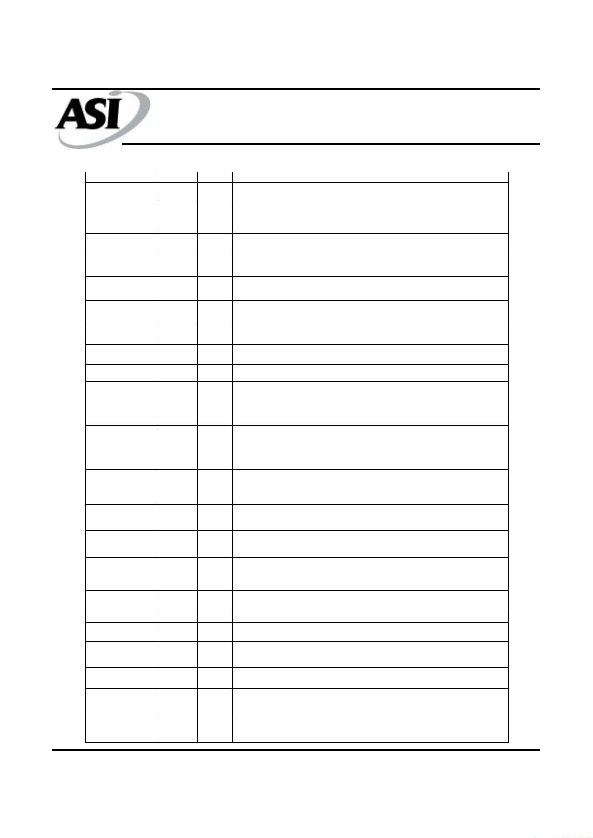
PIN DESCRIPTIONS
PIN NUMBERS SYM TYPE DESCRIPTION
37, 36, 32-35, 44-50,
80-82, 99, 100
SA0, SA1, SA Input Synchronous Address Inputs: These inputs are registered and must meet the setup and
hold times around the rising edge of CLK.
93, 94 BWa\
BWb\
Input Synchronous Byte Write Enables: These active LOW inputs allow individual bytes to be
written and must meet the setup and hold times around the rising edge of CLK. A byte
write enables is LOW for a WRITE cycle and HIGH for a READ cycle. BWa\ controls DQa
pins and DQPa; BWb\ controls DQb pins and DQPb.
87 BWE\ Input Byte Write Enable: This active LOW input permits BYTE WRITE operations and must meet
the setup and hold times around the rising edge of CLK.
88 GW\ Input Global Write: This active LOW input allows a full 18-bit WRITE to occur independent of the
BWE\ and BWx\ lines and must meet the setup and hold times around the rising edge of
CLK.
89 CLK Input Clock: This signal registers the addresses, data, chip enables, byte write enables and burst
control inputs on its rising edge. All synchronous inputs must meet setup and hold times
around the clock’s risin
g
edge.
98 CE\ Input Synchronous Chip Enable: This active LOW input is used to enable the device and
Conditions the internal use of ADSP\. CE\ is sampled only when a new external address is
loaded.
92 CE2\ Input Synchronous Chip Enable: This active LOW input is used to enable the device and is
sampled only when a new external address is loaded.
97 CE2 Input Synchronous Chip Enable: This active HIGH input is used to enable the device and is
sampled only when a new external address is loaded.
86 OE\ Input Output Enable: This active LOW, asynchronous input enables the data I/O output drivers.
83 ADV\ Input Synchronous Address Advance: This active LOW input is used to advance the internal
burst counter, controlling burst access after the external address is loaded. A HIGH on this
pin effectively causes wait states to be generated (no address advance). To ensure use of
correct address during WRITE cycle, ADV\ must be HIGH at the rising edge of the first
clock after an ADSP\ cycle is initiated.
84 ADSP\ Input Synchronous Address Status Processor: This active LOW input interrupts any ongoing
burst, causing a new external address to be registered. A READ is performed using the
new address, independent of the byte write enables and ADSC\, but dependent upon CE\,
CE2, and CE2\. ADSP\ is ignored if CE\ is HIGH. Power-down state is entered if CE2 if
LOW or CE2\ is HIGH.
85 ADSC\ Input Synchronous Address Status Controller: This active LOW input interrupts any ongoing
burst, causing a new external address to be registered. A READ or WRITE is performed
using the new address if CE\ is LOW. ADSC\ is also used to place the chip into powerdown state when CE\ is HIGH.
31 MODE Input Mode: This input selects the burst sequence. A LOW on this pin selects LINEAR BURST. A
NC or HIGH on this pin selects INTERLEAVED BURST. Do not alter input state while
device is operating.
64 ZZ Input Snooze Enable: This active HIGH, asynchronous input causes the device to enter a low-
power standby mode in which all data in the memory array is retained. When ZZ is active,
all other inputs are ignored.
(a) 58, 59, 62, 63, 68,
69, 72, 73
(b) 8, 9, 12,13, 18, 19,
22
,
23
DQa
DQb
Input/
Output
SRAM Data I/Os: Byte "a" is DQa pins; Byte "b" is DQb pins. Input data must meet setup
and hold times around the rising edge of CLK.
74, 24 NC/DQPa
NC/DQPb
NC/ I/O No Connect/Parity Data I/Os: Byte "a" is DQPa pins; Byte "b" is DQPb pins.
15, 41,65, 91 VDD Supply Power Supply: See DC Electrical Characteristics and Operating Conditions for range.
4, 11, 20, 27, 54, 61,
70, 77
VDDQ Supply Isolated Output Buffer Supply: See DC Electrical Characterics and Operating Conditions for
range.
5, 10, 14, 17, 21, 26,
40, 55, 60, 67 71, 76,
90
VSS Supply Ground: GND
38, 39 DNU --- Do Not Use: These signals may either be unconnected or wired to GND to improve
package heat dissipation.
1-3, 6, 7, 16,25, 28-30,
51-53, 56,57, 66, 75,
78, 79, 95, 96
NC ----- No Connect: These signals are not internally connected and may be connected to ground to
improve package heat dissipation.
42, 43 NF No Function: These pins are internally connected to the die and will have the capacitance of
input pins. It is allowable to leave these pins unconnected or driven by signals.
Page 3
AS5SS256K18
Rev. 2.0 12/00
Austin Semiconductor, Inc. reserves the right to change products or specifications without notice.
3
SSRAM
AS5SS256K18
Austin Semiconductor, Inc.
INTERLEAVED BURST ADDRESS TABLE (MODE=NC OR HIGH)
LINEAR BURST ADDRESS TABLE (MODE=LOW)
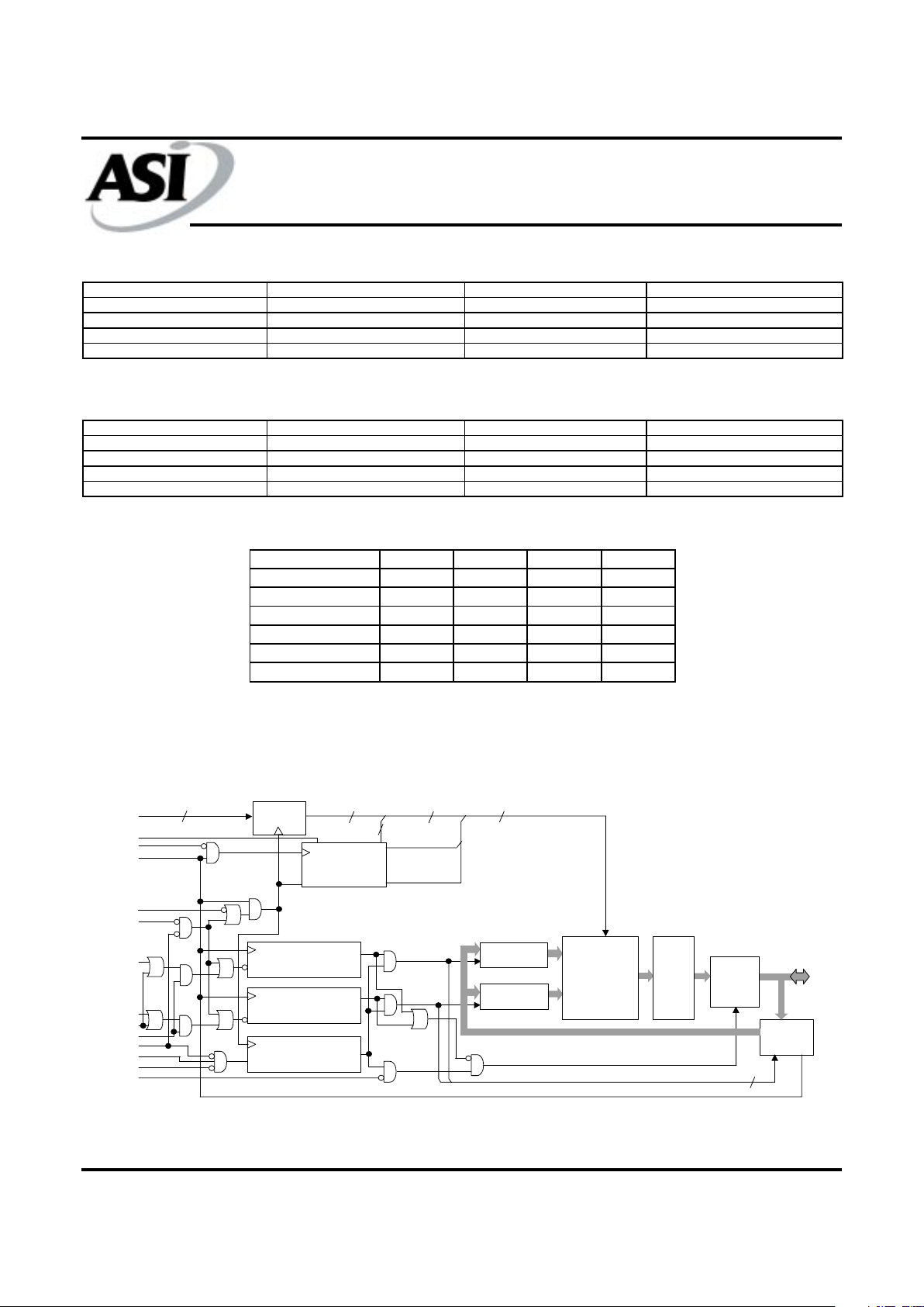
FUNCTIONAL BLOCK DIAGRAM
NOTE: The Functional Block Diagram illustrates simplified device operation. See T ruth T able, pin descriptions and timing
diagrams for detailed information.
18 18 16 18
SA0, SA1, SA
MODE
ADV\
CLK
ADSC\
ADSP\
BWb\
BWa\
BWE\
GW\
CE\
CE2
CE2\
OE\ 2
ADDRESS
REGISTER
BINARY
COUNTER AND
LOGIC
BYTE "b"
WRITE REGISTER
BYTE "a"
WRITE REGISTER
ENABLE
REGISTER
CLR
Q1
Q0
SA1'
SA0'
INPUT
REGISTERS
OUTPUT
BUFFERS
SENSE
AMPS
256K x 9 x 2
MEMORY
ARRAY
9
9
BYTE "b"
WRITE DRIVER
BYTE "a"
WRITE DRIVER
9
9
18
18
18
18
DQs
DQPa
DQPb
2
SA0-SA1
FIRST ADDRESS (EXTERNAL) SECOND ADDRESS (INTERNAL) THIRD ADDRESS (INTERNAL) FOURTH ADDRESS (INTERNAL)
X…X00 X…X01 X…X10 X…X11
X…X01 X…X00 X…X11 X…X10
X…X10 X…X11 X…X00 X…X01
X…X11 X…X10 X…X01 X…X00
FIRST ADDRESS (EXTERNAL) SECOND ADDRESS (INTERNAL) THIRD ADDRESS (INTERNAL) FOURTH ADDRESS (INTERNAL)
X…X00 X…X01 X…X10 X…X11
X…X01 X…X10 X…X11 X…X00
X…X10 X…X11 X…X00 X…X01
X…X11 X…X00 X…X01 X…X10
PARTIAL TRUTH TABLE FOR WRITE COMMANDS
FUNCTION GW\ BWE\ BWa\ BWb\
READ H H X X
READ H L H H
WRITE Byte "a" H L L H
WRITE Byte "b" H L H L
WRITE All Bytes H L L L
WRITE All Bytes L X X X
NOTE: Using BWE\ and BWa\ through BWb\, any one or more bytes may be
written.
Page 4
AS5SS256K18
Rev. 2.0 12/00
Austin Semiconductor, Inc. reserves the right to change products or specifications without notice.
4
SSRAM
AS5SS256K18
Austin Semiconductor, Inc.
TRUTH TABLE
NOTES: 1. X means “Don’t Care.” \ means active LOW . H means logic HIGH. L means logic LOW.
2. For WRITE\, L means any one or more byte write enable signals (BWa\, BWb\) and BWE\ are LOW or GW\ is LOW. WRITE\ = H for all BWx\,
BWE\, GW\ HIGH.
3. BWa\ enables WRITEs to DQas and DQPa. BWb\ enables WRITEs to DQbs and DQPb.
4. All inputs except OE\ and ZZ must meet setup and hold times around the rising edge (LOW to HIGH) of CLK.
5. Wait states are inserted by suspending burst.
6. For a WRITE operation following a READ operation, OE\ must be HIGH before the input data setup time and held HIGH throughout the input
data hold time.
7. This device contains circuitry that will ensure the outputs will be in High-Z during power-up.
8. ADSP\ LOW always initiates an internal READ at the L-H edge of CLK. A WRITE is performed by setting one or more byte write enable signals
and BWE\ LOW or GW\ LOW for the subsequent L-H edge of CLK. Refer to WRITE timing diagram for clarification.
OPERATION
ADDRESS
USED
CE\ CE2\ CE2 ZZ ADSP\ ADSC\ ADV\ WRITE\ OE\ CLK DQ
DESELECT Cycle, Power-Down NONE H X X L X L X X X L-H High-Z
DESELECT Cycle, Power-Down NONE L X L L L X X X X L-H High-Z
DESELECT Cycle, Power-Down NONE L H X L L X X X X L-H High-Z
DESELECT Cycle, Power-Down NONE L X L L H L X X X L-H High-Z
DESELECT Cycle, Power-Down NONE L H X L H L X X X L-H High-Z
SNOOZE MODE, Power-Down NONE X X X H X X X X X X High-Z
READ Cycle, Begin Burst EXTERNAL L L H L L X X X L L-H Q
READ Cycle, Begin Burst EXTERNAL L L H L L X X X H L-H High-Z
WRITE Cycle, Begin Burst EXTERNAL L L H L H L X L X L-H D
READ Cycle, Begin Burst EXTERNAL L L H L H L X H L L-H Q
READ Cycle, Begin Burst EXTERNAL L L H L H L X H H L-H High-Z
READ Cycle, Continue Burst NEXT X X X L H H L H L L-H Q
READ Cycle, Continue Burst NEXT X X X L H H L H H L-H High-Z
READ Cycle, Continue Burst NEXT H X X L X H L H L L-H Q
READ Cycle, Continue Burst NEXT H X X L X H L H H L-H High-Z
WRITE Cycle, Continue Burst NEXT X X X L H H L L X L-H D
WRITE Cycle, Continue Burst NEXT H X X L X H L L X L-H D
READ Cycle, Suspend Burst CURRENT X X X L H H H H L L-H Q
READ Cycle, Suspend Burst CURRENT X X X L H H H H H L-H High-Z
READ Cycle, Suspend Burst CURRENT H X X L X H H H L L-H Q
READ Cycle, Suspend Burst CURRENT H X X L X H H H H L-H High-Z
WRITE Cycle, Suspend Burst CURRENT X X X L H H H L X L-H D
WRITE Cycle, Suspend Burst CURRENT H X X L X H H L X L-H D
Page 5

AS5SS256K18
Rev. 2.0 12/00
Austin Semiconductor, Inc. reserves the right to change products or specifications without notice.
5
SSRAM
AS5SS256K18
Austin Semiconductor, Inc.
ABSOLUTE MAXIMUM RA TINGS*
Voltage on VDD Supply Relative to VSS............-0.5V to +4.6V
Voltage on VDDQ Supply Relative to VSS.........-0.5V to +4.6V
Storage Temperature (plastic) .....................-55 °C to +125°C
Max Junction T emperature**.......................................+150°C
Short Circuit Output Current..........…...........................100mA
*Stresses greater than those listed under "Absolute Maximum Ratings"
may cause permanent damage to the device. This is a stress rating only
and functional operation of the device at these or any other conditions
above those indicated in the operational sections of this specification is
not implied. Exposure to absolute maximum rating conditions for extended periods may affect reliability .
**Maximum junction temperature depends upon package type, cycle
time, loading, ambient temperature and airflow.
DC ELECTRICAL CHARACTERISTICS AND RECOMMENDED OPERATING CONDITIONS
(-55oC < TA < +125oC and -40oC<TA<+85oC; VDD = +3.3V +0.3V/-0.165V unless otherwise noted)
DESCRIPTION CONDITIONS SYMBOL MIN MAX UNITS NOTES
Input High (Logic 1) Voltage
V
IH
2.0
V
DD
+0.3
V 1, 2
Input Low (Logic 0) Voltage
V
IL
-0.3 0.8 V 1, 2
Input Leakage Current
(0V<
VIN<VDD)
IL
I
-2 2 µΑ
3
Output Leakage Current
Output(s) disabled;
0V<
VIN<V
DD
IL
O
-2 2 µΑ
Output High Voltage
I
OH
= -4.0mA V
OH
2.4 -- V 1, 4
Output Low Voltage
I
OL
= 8.0 mA V
OL
-- 0.5 V 1, 4
Supply Voltage
V
DD
3.135 3.6 V 1
Isolated Output Buffer Supply
V
DD
Q
3.135 3.6 V 1, 5
NOTES:
1. All voltages referenced to VSS (GND)
2. Overshoot: VIH < +4.6V for t < tKC/2 for I < 20mA
Undershoot: VIL > -0.7V for t < tKC/2 for I < 20mA
Power-up: VIH < +3.6V and VDD<3.135V for t < 200ms
3. MODE pin has an internal pull-up, and input leakage = ±10µA.
4. The load used for VOH, VOL testing is shown in Figure 2 for 3.3V I/O. AC load current is higher then the stated DC values.
5. VDDQ should never exceed VDD. VDD and VDDQ can be connected together, for 3.3V I/O operation only.
6. This parameter is sampled.
CAP A CIT ANCE
DESCRIPTION CONDITIONS SYM MAX UNITS NOTES
Control Input Capacitance
C
I
4pF6
Input/Output Capacitance (DQ)
C
O
5pF6
Address Capacitance
C
A
3.5 pF 6
Clock Capacitance
C
CK
3.5 pF 6
T
A
= 25°C; f = 1MHz;
V
DD
= 3.3V
THERMAL RESIST ANCE
DESCRIPTION CONDITIONS SYM TYP UNITS NOTES
Thermal Resistance
(Junction to Ambient)
θ
JA
46 °C/W 6
Thermal Resistance
(Junction to Top of Case)
θ
JC
2.8 °C/W 6
Test conditions follow standard test
methods and procedures for measuring
thermal impedance, per EIA/JESD51
Page 6

AS5SS256K18
Rev. 2.0 12/00
Austin Semiconductor, Inc. reserves the right to change products or specifications without notice.
6
SSRAM
AS5SS256K18
Austin Semiconductor, Inc.
IDD ELECTRICAL CHARACTERISTICS AND RECOMMENDED OPERATING CONDITIONS
(-55oC < TA < +125oC and -40oC<TA<+85oC; VDD = +3.3V +0.3V/-0.165V unless otherwise noted)
CONDITIONS SYM -8 -9 -10 UNITS NOTES
Device selected; all inputs <
VIL or > VIH;
Cycle time >
tKC (MIN); VDD = MAX; Outputs Open
I
DD
375 325 250 mA 2, 3, 4
Power Supply Current:
Idle
Device selected; VDD = MAX; ADSC\, ADSP\,
ADV\, GW\, BWx\ >
VIH; All inputs < VSS +0.2 or
>
VDDQ -0.2; Cycle time > tKC (MIN);
Outputs Open
I
DD1
100 85 65 mA 2, 3, 4
CMOS Standby
Device deselected; V
DD
= MAX;
All inputs <
Vss +0.2 or > VDDQ -0.2;
All inputs static; CLK frequency =0
I
SB2
10 10 10 mA 3, 4
TTL Standby
Device deselected; V
DD
= MAX;
All inputs <
VIL or > VIH;
All inputs static; CLK frequency = 0
I
SB3
25 25 25 mA 3, 4
Clock Running
Device deselected; V
DD
= MAX;
ASDP\, ADV\, GW\, BWx\ >
VIH;
All inputs <
VSS +0.2 or > VDDQ -0.2;
Cycle time >
tKC (MIN)
I
SB4
100 85 65 mA 3, 4
Power Supply Current:
Operating
PARAMETER
MAX
NOTES:
1. VDDQ = +3.3V +0.3V/-0.165V for 3.3V I/O configuration.
2. IDD is specified with no output current and increases with faster cycle times. IDDQ increases with faster cycle
times and greater output loading.
3. “Device deselected” means device is in power-down mode as defined in the truth table. “Device selected” means
device is active (not in power-down mode).
4. Typical values are measured at 3.3V, 25°C and 15ns cycle time.
Page 7

AS5SS256K18
Rev. 2.0 12/00
Austin Semiconductor, Inc. reserves the right to change products or specifications without notice.
7
SSRAM
AS5SS256K18
Austin Semiconductor, Inc.
ELECTRICAL CHARACTERISTICS AND RECOMMENDED AC OPERATING CONDITIONS
(Note 1) -55oC < TA < +125oC and -40oC<TA<+85oC; VDD = +3.3V +0.3V/-0.165V unless otherwise noted)
MIN MAX MIN MAX MIN MAX
Clock cycle time
t
KC
8.8 10 15 ns
Clock frequency
t
KF
113 100 66 MHz
Clock HIGH time
t
KH
2.5 3.0 4.0 ns 2
Clock LOW time
t
KL
2.5 3.0 4.0 ns 2
Clock to output valid
t
KQ
7.5 8.5 10 ns
Clock to output invalid
t
KQX
1.5 3.0 3.0
ns
3
Clock to output in Low-Z
t
KQLZ
1.5 3.0 3.0
ns
3, 4, 5
Clock to output in High-Z
t
KQHZ
4.2 5.0 5.0
ns
3, 4, 5
OE\ to output valid
t
OEQ
4.2 5.0 5.0
ns
6
OE\ to output in Low-Z
t
OELZ
000
ns
3, 4, 5
OE\ to output in High-Z
t
OEHZ
4.2 5.0 5.0
ns
3, 4, 5
Address
t
AS
1.5 1.8 2.0
ns
7, 8
Address status (ADSC\, ADSP\)
t
ADSS
1.5 1.8 2.0
ns
7, 8
Address advance (ADV\)
t
AAS
1.5 1.8 2.0
ns
7, 8
Byte write enables (BWa\-BWb\, GW\, BWE\)
t
WS
1.5 1.8 2.0
ns
7, 8
Data-in
t
DS
1.5 1.8 2.0
ns
7, 8
Chip enable (CE\)
t
CES
1.5 1.8 2.0
ns
7, 8
Address
t
AH
0.5 0.5 0.5
ns
7, 8
Address status (ADSC\, ADSP\)
t
ADSH
0.5 0.5 0.5
ns
7, 8
Address advance (ADV\)
t
AAH
0.5 0.5 0.5
ns
7, 8
Byte write enables (BWa\-BWb\, GW\, BWE\)
t
WH
0.5 0.5 0.5
ns
7, 8
Data-in
t
DH
0.5 0.5 0.5
ns
7, 8
Chip enable (CE\)
t
CEH
0.5 0.5 0.5
ns
7, 8
OUTPUT TIMES
SETUP TIMES
HOLD TIMES
NOTESUNITSSYMBOL
CLOCK
DESCRIPTION
-9-8 -10
NOTES:
1. T est conditions as specified with the output loading shown in Figure 1 for 3.3V I/O (VDDQ = +3.3V +0.3V/-0.165V) unless otherwise
noted.
2. Measured as HIGH above VIH and LOW below VIL.
3. This parameter is measured with the output loading shown in Figure 2 for 3.3V I/O.
4. This parameter is sampled.
5. Transition is measured ±500mV from steady state voltage.
6. OE\ is a “Don’t Care” when a byte write enable is sampled LOW.
7. A READ cycle is defined by byte write enables all HIGH or ADSP\ LOW for the required setup and hold times. A WRITE cycle is
defined by at least one byte write enable LOW and ADSP\ HIGH for the required setup and hold times.
8. This is a synchronous device. All addresses must meet the specified setup and hold times for all rising edges of CLK when either ADSP\ or
ADSC\ is LOW and chip enabled. All other synchronous inputs must meet the setup and hold times with stable logic levels for all rising edges
of clock (CLK) when the chip is enabled. Chip enable must be valid at each rising edge of CLK when either ADSP\ or ADSC\ is LOW to
remain enabled.
Page 8

AS5SS256K18
Rev. 2.0 12/00
Austin Semiconductor, Inc. reserves the right to change products or specifications without notice.
8
SSRAM
AS5SS256K18
Austin Semiconductor, Inc.
AC TEST CONDITIONS
OUTPUT LOADS
VIH = (VDD/2.2) + 1.5V
V
IL
= (VDD/2.2) - 1.5V
Input rise and fall times 1ns
Input timing reference levels
V
DD
/2.2
Output reference levels
V
DD
Q/2.2
Output load See Figures 1 and 2
Input pulse levels
3.3v
DQ
Fig. 2 OUTPUT LOAD EQUIVALENT
351Ω
5 pF
317Ω
Fig. 1 OUTPUT LOAD EQUIVALENT
DQ
50Ω
Z0=50Ω
Vt = 1.5V
LOAD DERATING CURVES
ASI’s 256K x 18 Synchronous Burst SRAM timing is dependent upon
the capacitive loading on the outputs.
SNOOZE MODE
SNOOZE MODE is a low-current, “power-down” mode in which the
device is deselected and current is reduced to I
SB2Z
. The duration of
SNOOZE MODE is dictated by the length of time ZZ is in a HIGH
state. After the device enters SNOOZE MODE, all inputs except ZZ
become gated inputs and are ignored.
ZZ is an asynchronous, active HIGH input that causes the device to
enter SNOOZE MODE. When ZZ becomes a logic HIGH, I
SB2Z
is
guaranteed after the setup time tZZ is met. Any READ or WRITE
operation pending when the device enters SNOOZE MODE is not
quaranteed to complete successfully. Therefore, SNOOZE MODE
must not be initiated until valid pending operations are completed.
* Except ZZ
23
4
23
4
23
4
Don’t Care
SNOOZE MODE W A VEFORM
DESCRIPTION CONDITIONS SYM MIN MAX UNITS NOTES
Current during SNOOZE MODE
ZZ >
V
IH
I
SB2Z
10 mA
ZZ active to input ignored
t
ZZ
t
KC
ns 1
ZZ inactive to input sampled
t
RZZ
t
KC
ns 1
ZZ active to snooze current
t
ZZI
t
KC
ns 1
ZZ inactive to exit snooze current
t
RZZI
0ns1
SNOOZE MODE ELECTRICAL CHARACTERISTICS
NOTE: 1. This parameter is sampled.
23456789
0
23456789
0
t
ZZ
t
RZZ
t
ZZI
I
SB2
t
RZZI
CLK
ZZ
I
SUPPLY
ALL INPUTS*
Page 9

AS5SS256K18
Rev. 2.0 12/00
Austin Semiconductor, Inc. reserves the right to change products or specifications without notice.
9
SSRAM
AS5SS256K18
Austin Semiconductor, Inc.
READ TIMING
NOTE: 1. Q(A2) referes to output from address A2. Q(A2+1) refers to output from the next internal burst address following A2.
2. CE2\ and CE2 have timing identical to CE\. On this diagram, when CE\ is LOW, CE2\ is LOW and CE2 is HIGH. When CE\ is HIGH, CE2\ is HIGH and CE2 is LOW.
3. Timing is shown assuming that the device was not enabled before entering into this sequence.
4. Outputs are disabled t
KQHZ
after deselect.
READ TIMING PARAMETERS
MIN MAX MIN MAX MIN MAX MIN MAX MIN MAX MIN MAX
t
KC
8.8 10 15 ns
t
AS
1.5 1.8 2.0 ns
t
KF
113 100 66 MHz
t
ADSS
1.5 1.8 2.0 ns
t
KH
2.5 3.0 4.0 ns
t
AAS
1.5 1.8 2.0 ns
t
KL
2.5 3.0 4.0 ns
t
WS
1.5 1.8 2.0 ns
t
KQ
7.5 8.5 10 ns
t
CES
1.5 1.8 2.0 ns
t
KQX
1.5 3.0 3.0 ns
t
AH
0.5 0.5 0.5 ns
t
KQLZ
1.5 3.0 3.0 ns
t
ADSH
0.5 0.5 0.5 ns
t
KQHZ
4.2 5.0 5.0 ns
t
AAH
0.5 0.5 0.5 ns
t
OEQ
4.2 5.0 5.0 ns
t
WH
0.5 0.5 0.5 ns
t
OELZ
000 ns
t
CEH
0.5 0.5 0.5 ns
t
OEHZ
4.2 5.0 5.0 ns
-10-9-8
SYM
-10
UNITSUNITS SYM
-8 -9
2345678
9
2345678
9
2345678
9
2345678
9
2345678
9
2345678
9
2345678
9
2345678
9
23456
7
23456
7
23456
7
23456
7
23456
7
CLK
ADSP\
ADSC\
○○○○○○○○○○○○○○○○○○○○○○○○○○○○○○○○○○○○○○○○○
○○○○○○○○○○○○○○○○○○○○○○○○○○○○○○○○○○○○○○○○○
○○○○○○○○○○○○○○○○○○○○○○○○○○○○○○○○○○○○○○○○○
○○○○○○○○○○○○○○○○○○○○○○○○○○○○○○○○○○○○○○○○○
○○○○○○○○○○○○○○○○○○○○○○○○○○○○○○○○○○○○○○○○○
○○○○○○○○○○○○○○○○○○○○○○○○○○○○○○○○○○○○○○○○○
○○○○○○○○○○○○○○○○○○○○○○○○○○○○○○○○○○○○○○○○○
○○○○○○○○○○○○○○○○○○○○○○○○○○○○○○○○○○○○○○○○○
○○○○○○○○○○○○○○○○○○○○○○○○○○○○○○○○○○○○○○○○○
○○○○○○○○○○○○○○○○○○○○○○○○○○○○○○○○○○○○○○○○○
ADDRESS
A2
BWE\, GW\,
BWa\-BWb\
○○○○○○○○○○○○○○○○○○○○○○○○○○○○○○○○○○○○○○○○○
CE\
(Note 2)
ADV\
OE\
SINGLE READ BURST READ
○○○○○○○○○○○○○○○○○○○○○○○○○○○○○○○○○○○○○○○○○
Q
A1
2
3
2
3
2
3
2
3
234567890123456789012345678901212345678901234567890123456789012123456789012345678
9
234567890123456789012345678901212345678901234567890123456789012123456789012345678
9
234567890123456789012345678901212345678901234567890123456789012123456789012345678
9
234567890123456789012345678901212345678901234567890123456789012123456789012345678
9
Q(A2)
Q(A2+2)
Q(A2+3)
Q(A2)
Q(A2+1)
Q(A2+2)
234567
8
234567
8
234567
8
234567
8
Q(A1)
Q(A2+1)
23456789012345678901
2
23456789012345678901
2
23456789012345678901
2
23456789012345678901
2
23456789012345678901
2
23456789012345678901
2
23456789012345678901
2
23456789012345678901
2
23456789012345678901
2
2345
6
2345
6
2345
6
2345
6
2345
6
t
ADSS
t
ADSH
t
AS
t
AH
t
KC
t
KL
t
KH
t
ADSS
t
ADSH
t
WS
t
WH
t
CES
t
CEH
t
AAS
t
AAH
ADV\ suspends burst.
High-Z
t
OEHZ
t
KQLZ
t
KQ
t
OEQ
t
OELZ
t
KQ
t
KQX
t
KQHZ
Burst wraps around
to its initial state.
(NOTE 1)
Deselect Cycle
(Note 4)
Page 10

AS5SS256K18
Rev. 2.0 12/00
Austin Semiconductor, Inc. reserves the right to change products or specifications without notice.
10
SSRAM
AS5SS256K18
Austin Semiconductor, Inc.
NOTE: 1. D(A2) refers to output from address A2. D(A2+1) refres to output from the next internal burst address following A2.
2. CE2\ and CE2 have timing identical to CE\. On this diagram, when CE\ is LOW, CE2\ is LOW and CE2 is HIGH. When CE\ is HIGH, CE2\ is HIGH and CE2 is LOW.
3. OE\ must be HIGH before the input data setup and held HIGH throughout the data hold time. This prevents input/output data contention for the time period
prior to the byte write enable inputs being sampled.
4. ADV\ must be HIGH to permit a WRITE to the loaded address.
5. Full-width WRITE can be initiated by GW\ LOW; or GW\ HIGH and BWE\, BWa\ and BWb\ LOW.
WRITE TIMING
MIN MAX MIN MAX MIN MAX MIN MAX MIN MAX MIN MAX
t
KC
8.8 10 15 ns
t
DS
1.5 1.8 2.0 ns
t
KF
113 100 66 MHz
t
CES
1.5 1.8 2.0 ns
t
KH
2.5 3.0 4.0 ns
t
AH
0.5 0.5 0.5 ns
t
KL
2.5 3.0 4.0 ns
t
ADSH
0.5 0.5 0.5 ns
t
OEHZ
4.2 5.0 5.0 ns
t
AAH
0.5 0.5 0.5 ns
t
AS
1.5 1.8 2.0 ns
t
WH
0.5 0.5 0.5 ns
t
ADSS
1.5 1.8 2.0 ns
t
DH
0.5 0.5 0.5 ns
t
AAS
1.5 1.8 2.0 ns
t
CEH
0.5 0.5 0.5 ns
t
WS
1.5 1.8 2.0 ns
-10-9-8
SYM
-10
UNITSUNITS SYM
-8 -9
WRITE TIMING P ARAMETERS
2345678
9
2345678
9
2345678
9
2345678
9
23456789
0
23456789
0
23456789
0
23456789
0
23456789
0
23456789
0
23456789
0
23456789
0
23456789
0
2345
6
2345
6
2345
6
2345
6
2345
6
2345678
9
2345678
9
2345678
9
2345678
9
23456789
0
23456789
0
23456789
0
23456789
0
2345678
9
2345678
9
2345678
9
2345678
9
2345678
9
2345678
9
2345678
9
2345678
9
23456789
0
23456789
0
23456789
0
23456789
0
23456789
0
2345678
9
2345678
9
2345678
9
2345678
9
2345678
9
CLK
ADSP\
ADSC\
○○○○○○○○○○○○○○○○○○○○○○○○○○○○○○○○○○○○○○○
○○○○○○○○○○○○○○○○○○○○○○○○○○○○○○○○○○○○○○○○
○○○○○○○○○○○○○○○○○○○○○○○○○○○○○○○○○○○○○○○○
○○○○○○○○○○○○○○○○○○○○○○○○○○○○○○○○○○○○○○○○
○○○○○○○○○○○○○○○○○○○○○○○○○○○○○○○○○○○○○○○○
○○○○○○○○○○○○○○○○○○○○○○○○○○○○○○○○○○○○○○○○
○○○○○○○○○○○○○○○○○○○○○○○○○○○○○○○○○○○○○○○○
○○○○○○○○○○○○○○○○○○○○○○○○○○○○○○○○○○○○○○○○
○○○○○○○○○○○○○○○○○○○○○○○○○○○○○○○○○○○○○○○○
○○○○○○○○○○○○○○○○○○○○○○○○○○○○○○○○○○○○○○○○
ADDRESS
A2
BEW\,
BWa\ - BWb\
○○○○○○○○○○○○○○○○○○○○○○○○○○○○○○○○○○○○○○○
CE\
(NOTE 2)
ADV\
OE\
SINGLE WRITE
BURST WRITE
GW\
○○○○○○○○○○○○○○○○○○○○○○○○○○○○○○○○○○○○○○○○
D
Extended
BURST WRITE
A1
2
3
2
3
2
3
2
3
23456789012345678901234567890121234567890123
4
23456789012345678901234567890121234567890123
4
23456789012345678901234567890121234567890123
4
23456789012345678901234567890121234567890123
4
23456789012345678901234567890121234567890123
4
A3
2345678901234567890
1
2345678901234567890
1
2345678901234567890
1
2345678901234567890
1
2345678901234567890
1
23456789012345678901234567890121234567890123456789012345678901212345678901
2
23456789012345678901234567890121234567890123456789012345678901212345678901
2
23456789012345678901234567890121234567890123456789012345678901212345678901
2
23456789012345678901234567890121234567890123456789012345678901212345678901
2
D(A2)
D(A2+2)
D(A2+3)
D(A3)
D(A3+1)
D(A3+2)
23456
7
23456
7
23456
7
23456
7
23456
7
23456789012345678901234567890121234567890123456789
0
23456789012345678901234567890121234567890123456789
0
23456789012345678901234567890121234567890123456789
0
23456789012345678901234567890121234567890123456789
0
23456789012345678901234567890121234567890123456789
0
23456789012345678901234
5
23456789012345678901234
5
23456789012345678901234
5
23456789012345678901234
5
23456789012345678901234
5
D(A1)
D(A2+1)
t
ADSS
t
ADSH
t
KC
t
KL
t
KH
t
AS
t
AH
t
ADSS
t
ADSH
ADSC\ extends burst.
BYTE WRITE signals are ignored
when ADSP\ is LOW.
t
WS
t
WH
tWSt
WH
(Note 5)
234
5
234
5
234
5
234
5
t
CEStCEH
t
AAS
t
AAH
(Note 4)
ADV\ suspends burst.
(Note 3)
Q
12345
6
t
OEHZ
D(A2+1)
(Note 1)
High-Z
BURST READ
234
5
234
5
Don’t Care
t
DS
t
DH
Page 11

AS5SS256K18
Rev. 2.0 12/00
Austin Semiconductor, Inc. reserves the right to change products or specifications without notice.
11
SSRAM
AS5SS256K18
Austin Semiconductor, Inc.
NOTE: 1. Q(A4) refers to output from address A4. Q(A4+1) refers to output from the next internal burst address following A4.
2. CE2\ and CE2 have timing identical to CE\. On this diagram, when CE\ is LOW, CE2\ is LOW and CE2 is HIGH. When CE\ is HIGH, CE2\ is HIGH and CE2 is LOW.
3. The data bus (Q) remains in High-Z following a WRITE cycle unless an ADSP\, ADSC\, or ADV\ cycle is performed.
4. GW\ is HIGH.
5. Back-to-back READs may be controlled by either ADSP\ or ADSC\.
6. Timing is shown assuming that the device was not enabled before entering into this sequence.
READ/WRITE TIMING
6
MIN MAX MIN MAX MIN MAX MIN MAX MIN MAX MIN MAX
t
KC
8.8 10 15 ns
t
WS
1.5 1.8 2.0 ns
t
KF
113 100 66 MHz
t
DS
1.5 1.8 2.0 ns
t
KH
2.5 3.0 4.0 ns
t
CES
1.5 1.8 2.0 ns
t
KL
2.5 3.0 4.0 ns
t
AH
0.5 0.5 0.5 ns
t
KQ
7.5 8.5 10 ns
t
ADSH
0.5 0.5 0.5 ns
t
OELZ
000 ns
t
WH
0.5 0.5 0.5 ns
t
OEHZ
3.5 4.2 5.0 ns
t
DH
0.5 0.5 0.5 ns
t
AS
1.5 1.8 2.0 ns
t
CEH
0.5 0.5 0.5 ns
t
ADSS
1.5 1.8 2.0 ns
-10-9-8
SYM
-10
UNITSUNITS SYM
-8 -9
READ/WRITE PARAMETERS
2345678
9
2345678
9
2345678
9
2345678
9
2345678
9
CLK
ADSP\
ADSC\
○○○○○○○○○○○○○○○○○○○○○○○○○○○○○○○○○○
○○○○○○○○○○○○○○○○○○○○○○○○○○○○○○○○○○
○○○○○○○○○○○○○○○○○○○○○○○○○○○○○○○○○○
○○○○○○○○○○○○○○○○○○○○○○○○○○○○○○○○○○○○
○○○○○○○○○○○○○○○○○○○○○○○○○○○○○○○○○○
○○○○○○○○○○○○○○○○○○○○○○○○○○○○○○○○○○
○○○○○○○○○○○○○○○○○○○○○○○○○○○○○○○○○○
○○○○○○○○○○○○○○○○○○○○○○○○○○○○○○○○○○
○○○○○○○○○○○○○○○○○○○○○○○○○○○○○○○○○○
○○○○○○○○○○○○○○○○○○○○○○○○○○○○○○○○○○
ADDRESS
A2
BWE\, GW\
BWa\ - BWb\
○○○○○○○○○○○○○○○○○○○○○○○○○○○○○○○○○○
CE\
(Note 2)
ADV\
OE\
Back-to-Back READS
(NOTE 5)
BURST READ
○○○○○○○○○○○○○○○○○○○○○○○○○○○○○○○○○○
D
Back-to-Back
WRITEs
2
3
2
3
2
3
2
3
234567890123456789012345678901212
3
234567890123456789012345678901212
3
234567890123456789012345678901212
3
234567890123456789012345678901212
3
A5
D(A5) D(A6)
123456789012345678901234567890121234567
8
123456789012345678901234567890121234567
8
123456789012345678901234567890121234567
8
123456789012345678901234567890121234567
8
123456789012345678901234567890121234567
8
D(A3)
A1
A3
2
3
2
3
2
3
2
3
A4
234567890123456789012345678901212345678901
2
234567890123456789012345678901212345678901
2
234567890123456789012345678901212345678901
2
234567890123456789012345678901212345678901
2
SINGLE WRITE
t
KC
t
KL
t
KH
t
ADSS
t
ADSH
A6
t
AS
2345678
9
2345678
9
2345678
9
2345678
9
2345678
9
t
AH
2345678
9
2345678
9
2345678
9
2345678
9
2345678
9
t
CES
t
CEH
t
WS
t
WH
Q(A1)
Q(A2)
Q(A4) Q(A4+1)
Q(A4+2)
Q(A4+3)
Q
High-Z
tDSt
DH
t
OELZ
t
KQ
(NOTE 1)
2345
6
2345
6
2345
6
Don’t Care
234
5
234
5
234
5
Undefined
t
OEHZ
Page 12

AS5SS256K18
Rev. 2.0 12/00
Austin Semiconductor, Inc. reserves the right to change products or specifications without notice.
12
SSRAM
AS5SS256K18
Austin Semiconductor, Inc.
MECHANICAL DEFINITIONS
ASI Case #1001 (Package Designator DQ)
16.00 +0.20/-0.05
14.00 + 0.10
22.10 + 0.10/-0.15
20.10 + 0.10
0.62
Pin #1 ID
NOTE: 1. All dimensions in Millimeters (MAX/MIN) or typical where noted.
2. Package width and length do not include mold protrusion; allowable mold protursion is 0.25mm per side.
1.00 TYP
DET AIL A
0.10 +0.10/-0.05
Gage Plane
0.25
0.60 + 0.15
0.32 +0.06/-0.10
0.65
1.50 + 0.10
1.40 + 0.05
0.10
See Detail A
0.15 +0.03/-0.02
Page 13

AS5SS256K18
Rev. 2.0 12/00
Austin Semiconductor, Inc. reserves the right to change products or specifications without notice.
13
SSRAM
AS5SS256K18
Austin Semiconductor, Inc.
EXAMPLE: AS5SS256K18DQ-8/IT
Device Number
Package
Type
Speed ns Process
AS5SS256K18 DQ -8 IT only
AS5SS256K18 DQ -9 /*
AS5SS256K18 DQ -10 /*
ORDERING INFORMA TION
*AVAILABLE PROCESSES
IT = Industrial T emperature Range -40oC to +85oC
XT = Extended T emperature Range -55oC to +125oC
 Loading...