

Datasheet AS4LC1M16E5-60TI, AS4LC1M16E5-60TC, AS4LC1M16E5-60JI, AS4LC1M16E5-60JC, AS4LC1M16E5-50TI Datasheet (Alliance Semiconductor Corporation)
...Page 1
3V 1M×16 CMOS DRAM (EDO)
Features
• Organization: 1,048,576 words × 16 bits
• High speed
- 50/60 ns RAS access time
- 20/25 ns hyper page cycle time
- 12/15 ns CAS
• Low power consumption
- Active: 500 mW max (-60)
- Standby: 3.6 mW max, CMOS DQ
• Extended data out
• 1024 refresh cycles, 16 ms refresh interval
-RAS-only or CAS-before-RAS refresh or self-refresh
access time
AS4LC1M16E5
®
•Read-modify-write
• TTL-compatible, three-state DQ
• JEDEC standard package and pinout
- 400 mil, 42-pin SOJ
- 400 mil, 44/50-pin TSOP II
• 3V power supply (AS4LC1M16E5)
• 5V tolerant I/Os; 5.5V maximum V
• Industrial and commercial temperature available
IH
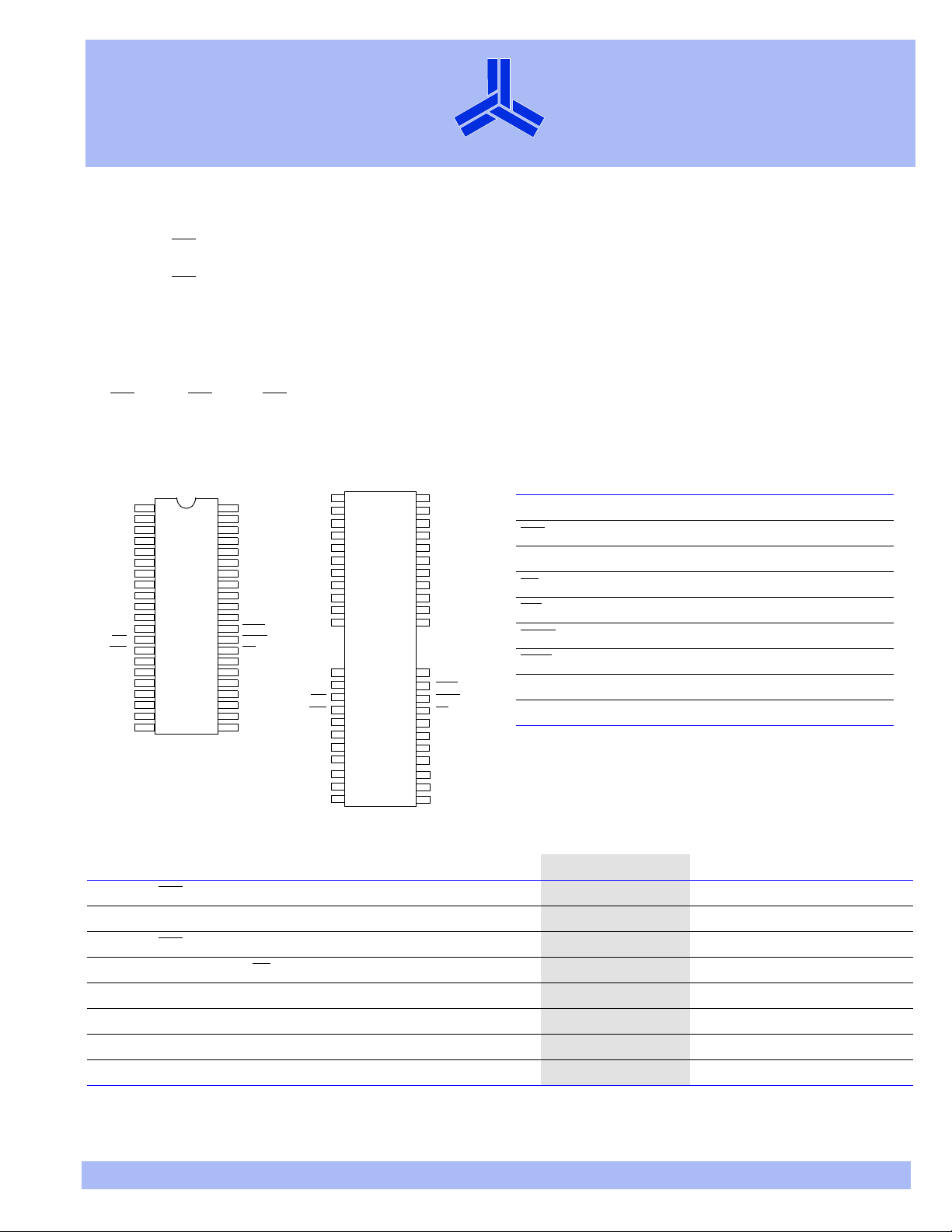
Pin arrangement
TSOP II
V
1
CC
2
3
4
5
CC
6
7
8
9
10
11
15
16
17
18
19
20
21
A0
22
A1
A2
23
A3
24
25
CC
50
SS
DQ16
49
DQ15
48
DQ14
47
DQ13
46
V
45
SS
DQ12
44
DQ11
43
DQ10
42
DQ9
41
NC
40
NC
36
LCAS
35
UCAS
34
OE
33
32
A9
31
A8
30
A7
29
A6
A5
28
A4
27
V
26
SS
Vcc
DQ1
DQ2
DQ3
DQ4
Vcc
DQ5
DQ6
DQ7
DQ8
NC
NC
WE
RAS
NC
NC
A0
A1
A2
A3
SOJ
1
2
3
4
5
6
7
8
9
10
11
12
13
14
15
16
17
18
19
20
SS
41
DQ16
40
DQ15
39
DQ14
38
DQ13
37
V
SS
36
DQ12
35
DQ11
34
DQ10
33
DQ9
32
NC
31
LCAS
30
UCAS
29
OE
28
A9
27
A8
26
A7
25
A6
24
A5
23
A4
2221Vcc
V
SS
V
42
V
DQ1
DQ2
DQ3
DQ4
V
DQ5
DQ6
DQ7
DQ8
NC
NC
NC
WE
RAS
NC
NC
V
Selection guide
Maximum RAS
Maximum column address access time t
Maximum CAS
Maximum output enable (OE
Minimum read or write cycle time t
Minimum hyper page mode cycle time t
Maximum operating current I
Maximum CMOS standby current I
Shaded areas indicate advance information.
access time t
access time t
) access time t
Pin designation
Pin(s) Description
A0 to A9 Address inputs
RAS
DQ1 to DQ16 Input/output
OE
WE
UCAS
LCAS
V
CC
V
SS
Symbol -50 -60 Unit
RAC
AA
CAC
OEA
RC
HPC
CC1
CC5
Row address strobe
Output enable
Write enable
Column address strobe, upper byte
Column address strobe, lower byte
Power
Ground
50 60 ns
25 30 ns
10 12 ns
10 12 ns
80 100 ns
20 25 ns
140 120 mA
1.0 1.0 mA
4/11/01; v.1.0
Alliance Semiconductor P. 1 of 22
Alliance Semiconductor
Copyright © Alliance Semiconductor. All rights reserved.
Page 2
AS4LC1M16E5
®
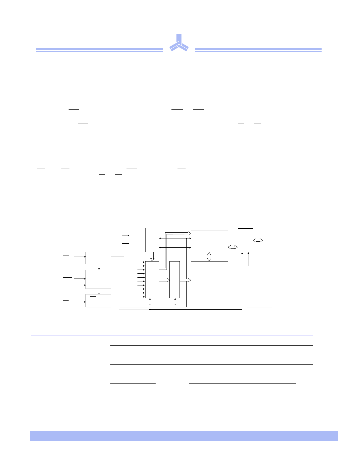
Functional description
The AS4LC1M16E5 is a high performance 16-megabit CMOS Dynamic Random Access Memory (DRAM) organized as 1,048,576 words × 16
bits. The device is fabricated using advanced CMOS technology and innovative design techniques resulting in high speed, extremely low power
and wide operating margins at component and system levels. The Alliance 16Mb DRAM family is optimized for use as main memory in
personal and portable PCs, workstations, and multimedia and router switch applications.
The AS4LC1M16E5 features hyper page mode operation where read and write operations within a single row (or page) can be executed at very
high speed by toggling column addresses within that row. Row and column addresses are alternately latched into input buffers using the falling
edge of RAS
addresses prior to xCAS
Extended data out (EDO), also known as 'hyper-page mode,' enables high speed operation. In contrast to 'fast-page mode' devices, data remains
active on outputs after xCAS
and prevent bus contention during read-modify-write and shared bus applications. Outputs also go to high impedance at the last occurrance of
RAS and xCAS going high.
Refresh on the 1024 address combinations of A0 to A9 must be performed every 16 ms using:
•RAS-only refresh: RAS is asserted while xCAS is held high. Each of the 1024 rows must be strobed. Outputs remain high impedence.
• Hidden refresh: xCAS
•CAS-before-RAS refresh (CBR): At least one xCAS is asserted prior to RAS. Refresh address is generated internally.
Outputs are high-impedence (OE
• Normal read or write cycles refresh the row being accessed.
• Self-refresh cycles
The AS4LC1M16E5 is available in the standard 42-pin plastic SOJ and 44/50-pin TSOP II packages, respectively. The AS4LC1M16E5 device
operates with a single power supply of 3V ± 0.3V and provides TTL compatible inputs and outputs.
and xCAS inputs, respectively. Also, RAS is used to make the column address latch transparent, enabling application of column
assertion. The AS4LC1M16E5 provides dual UCAS and LCAS for independent byte control of read and write access.
is de-asserted high, giving system logic more time to latch the data. Use OE and WE to control output impedance
is held low while RAS is toggled. Outputs remain low impedence with previous valid data.
and WE are don't care).
Logic block diagram
Data
DQ
buffers
Substrate bias
DQ1 to DQ16
OE
generator
RAS
UCAS
LCAS
WE
RAS clock
generator
CAS clock
generator
WE clock
generator
V
GND
CC
Refresh
controller
A0
A1
A2
A3
A4
A5
A6
A7
A8
A9
Address buffers
Row decoder
Column decoder
Sense amp
1024 × 1024 × 16
Array
(16,777,216)
Recommended operating conditions
Parameter Symbol Min Nominal Max Unit
V
Supply voltage
CC
GND 0.0 0.0 0.0 V
V
Input voltage
IH
V
IL
Commercial
Ambient operating temperature
Industrial -40 – 85
†
VIL min -3.0V for pulse widths less than 5 ns.
Recommended operating conditions apply throughout this document unless otherwise specified.
T
A
3.0 3.3 3.6 V
2.0 – 5.5 V
†
–0.5
–0.8V
0–70
°C
4/11/01 Alliance Semiconductor 2
Page 3

AS4LC1M16E5
®
Absolute maximum ratings
Parameter Symbol Min Max Unit
Input voltage V
Power supply voltage V
Storage temperature (plastic) T
Soldering temperature
time T
×
Power dissipation P
Short circuit output current I
DQ
CC
STG
SOLDER
D
out
-1.0 +5.5 V
-1.0 +4.0 V
-65 +150 °C
– 260 × 10
o
C × sec
–0.6W
–50mA
Truth table
Addresses
Operation RAS
LCAS UCAS WE OE
R
Standby H H to X H to X X X X X High-Z
Wo r d re a d LL LHLROWCOL Data out
Lower byte
read
Upper byte
read
Wo r d
(early) write
Lower byte
(early) write
Upper byte
(early) write
LLHHLROWCOL
LH LHLROWCOL
LL LLXROWCOL Data in
LLHLXROWCOL
LH L LXROWCOL
Read write L L L H to L L to H ROW COL Data out, Data in 1,2
1st cycle L H to L H to L H L ROW COL Data out 2
EDO read
2nd cycle L H to L H to L H L n/a COL Data out 2
Any cycle L L to H L to H H L n/a n/a Data out 2
1st cycle L H to L H to L L X ROW COL Data in 1
EDO write
EDO
read write
only
RAS
refresh
2nd cycle L H to L H to L L X n/a COL Data in 1
1st cycle L H to L H to L H to L L to H ROW COL Data out, Data in 1,2
2nd cycle L H to L H to L H to L L to H n/a COL Data out, Data in 1,2
L H H X X ROW n/a High Z
CBR refresh H to L L L H X X X High Z 3
Self refresh H to L L L H X X X High Z 3
t
C
DQ0 to DQ15 Notest
Lower byte,
Upper byte, Data out
Lower byte,
Data out, Upper byte
Lower byte, Data in, Upper byte, High-Z
Lower byte, High-Z,
Upper byte, Data in
4/11/01 Alliance Semiconductor 3
Page 4
DC electrical characteristics
Parameter Symbol Test conditions
Input leakag
urrent I
e c
Output leakage current I
Operating power
supply current
TTL standby power
supply current
I
I
Average power supply
current, RAS
refresh
I
mode or CBR
EDO page mode average
power supply current
CMOS standby power
supply current
I
I
V
Output voltage
V
before RAS refresh
CAS
current
I
Self refresh current I
Shaded areas indicate advance information.
0V ≤ Vin ≤ V
IL
Pins not under test = 0V
D
OL
disabled, 0V ≤ V
OUT
RAS, UCAS, LCAS, Address cycling;
CC1
t
=min
RC
RAS = UCAS = LCAS ≥ V
CC2
all other inputs at V
RAS cycling, UCAS = LCAS ≥ V
CC3
t
= min of RAS low after XCAS low.
RC
RAS = VIL, UCAS or LCAS,
CC4
address cycling: t
RAS = UCAS = LCAS = VCC - 0.2V,
CC5
F = 0
OHIOUT
OLIOUT
CC6
= -5.0 mA 2.4 –2.4– V
= 4.2 mA – 0.4 – 0.4 V
RAS, UCAS or LCAS cycling, tRC = min – 80 – 70
RAS = UCAS = LCAS ≤ 0.2V,
WE
CC7
= OE ≥ V
all other inputs at 0.2V or
V
- 0.2V
CC
(max)
CC
CC
IH
= min
HPC
- 0.2V,
out
or V
®
-50 -60
Min Max Min Max
-2 +2 -2 +2
≤ V
(max) -2 +2 -2 +2
CC
– 140 – 130 mA 4,5
,
IH
IL
,
IH
– 2.0 – 2.0 mA
– 80 – 70 mA 4
– 85 – 75 mA 4, 5
– 1–1mA
– 0.5 – 0.5
AS4LC1M16E5
Unit Notes
A
µ
A
µ
mA
mA
4/11/01 Alliance Semiconductor 4
Page 5
AS4LC1M16E5
®
AC parameters common to all waveforms
-50 -60
Symbol Parameter
t
RC
t
RP
t
RAS
t
CAS
t
RCD
t
RAD
t
RSH
t
CSH
t
CRP
t
ASR
t
RAH
t
T
t
REF
t
CP
t
RAL
Column address setup time 0 –0–ns
t
ASC
t
Column address hold time 8 –10–ns
CAH
Shaded areas indicate advance information.
Random read or write cycle time 80 –100–ns
RAS precharge time 30 –40–ns
RAS pulse width 50 10K 60 10K ns
CAS pulse width 8 10K 10 10K ns
RAS to CAS delay time 15 35 15 43 ns 9
RAS to column address delay time 9 25 10 30 ns 10
CAS to RAS hold time 10 –10–ns
RAS to CAS hold time 40 –50–ns
CAS to RAS precharge time 5 –5–ns
Row address setup time 0 –0–ns
Row address hold time 8 –10–ns
Transition time (rise and fall) 1 50150ns7,8
Refresh period – 16 – 16 ms 6
CAS precharge time 8 –10–ns
Column address to RAS lead time 25 –30–ns
Min Max Min Max
Unit Notes
Read cycle
Symbol Parameter
t
RAC
t
CAC
t
AA
t
RCS
t
RCH
t
RRH
Shaded areas indicate advance information.
Access time from RAS – 50 – 60 ns 9
Access time from CAS – 12 – 15 ns 9,16
Access time from address – 25 – 30 ns 10,16
Read command setup time 0 –0–ns
Read command hold time to CAS 0 –0–ns12
Read command hold time to RAS 0 –0–ns12
-50 -60
Min Max Min Max
Unit Notes
4/11/01 Alliance Semiconductor 5
Page 6
AS4LC1M16E5
®
Write cycle
-50 -60
Symbol Parameter
t
Write command setup time 0 –0–ns14
WCS
t
Write command hold time 10 –10– ns14
WCH
t
Write command pulse width 10 –10– ns
WP
t
Write command to RAS lead time 10 –10– ns
RW L
t
Write command to CAS lead time 8 –10– ns
CWL
Data-in setup time 0 –0–ns15
t
DS
t
Data-in hold time 8 –10– ns15
DH
Shaded areas indicate advance information.
Min Max Min Max
Unit Notes
Read-modify-write cycle
-50 -60
Symbol Parameter
t
Read-write cycle time 113 –135– ns
RW C
t
RAS to WE delay time 67 – 77 – ns 14
RW D
CAS to WE delay time 32 – 35 – ns 14
t
CWD
t
Column address to WE delay time 42 – 47 – ns 14
AW D
Shaded areas indicate advance information.
Min Max Min Max
Unit Notes
Refresh cycle
-50 -60
Symbol Parameter
t
CAS setup time (CAS-before-RAS
CSR
t
CAS hold time (CAS-before-RAS) 8 –10– ns6
CHR
t
RAS precharge to CAS hold time 0 –0–ns
RPC
precharge time
t
CPT
Shaded areas indicate advance information.
CAS
(CBR counter test)
)
Min Max Min Max
5 –5–ns6
10 –10– ns
Unit Notes
4/11/01 Alliance Semiconductor 6
Page 7
Hyper page mode cycle
Symbol Parameter
t
CPWD
t
CPA
t
RASP
t
DOH
t
REZ
t
WEZ
t
OEZ
t
HPC
t
HPRWC
t
RHCP
Shaded areas indicate advance information.
CAS precharge to WE delay time 45 –52–ns
Access time from CAS precharge – 28 – 35 ns 16
RAS pulse width 50 100K 60 100K ns
Previous data hold time from CAS 5 –5–ns
Output buffer turn off delay from RAS 0 13 0 15 ns
Output buffer turn off delay from WE 0 13 0 15 ns
Output buffer turn off delay from OE 0 13 0 15 ns
Hyper page mode cycle time 20 –25–ns
Hyper page mode RMW cycle 47 –56– ns
RAS hold time from CAS 30 –35– ns
Output enable
Symbol Parameter
t
CLZ
t
ROH
t
OEA
t
OED
t
OEZ
t
OEH
t
OLZ
t
OFF
Shaded areas indicate advance information.
CAS to output in Low Z 0 –0–ns11
RAS hold time referenced to OE 8 –10–ns
OE access time – 13 – 15 ns
OE to data delay 13 –15–ns
Output buffer turnoff delay from OE 0 13015ns11
OE command hold time 10 –10– ns
OE to output in Low Z 0 –0–ns
Output buffer turn-off time 0 13 0 15 ns 11,13
®
-50 -60
Min Max Min Max
-50 -60
Min Max Min Max
AS4LC1M16E5
Unit Notes
Unit Notes
Self refresh cycle
-50 -60
Std Symbol Parameter
t
RASS
t
RPS
t
CHS
Shaded areas indicate advance information.
4/11/01 Alliance Semiconductor 7
RAS pulse width
(CBR self refresh)
RAS precharge time
(CBR self refresh)
hold time
CAS
(CBR self refresh)
Min Max Min Max
100 –100– µs
90 –105– ns
8 –10– ns
Unit Notes
Page 8

®
(
)
Notes
1 Write cycles may be byte write cycles (either LCAS or UCAS active).
2 Read cycles may be byte read cycles (either LCAS
3One CAS
4I
5I
must be active (either LCAS or UCAS).
, I
, I
CC1
CC1
, and I
CC3
CC4
and I
depend on output loading. Specified values are obtained with the output open.
CC4
are dependent on frequency.
CC6
6 An initial pause of 200 µs is required after power-up followed by any 8 RAS
refresh counter, a minimum of 8 CAS
-before-RAS initialization cycles instead of 8 RAS cycles are required. 8 initialization cycles are required after
extended periods of bias without clocks (greater than 8 ms).
7 AC Characteristics assume t
8V
(min) and VIL (max) are reference levels for measuring timing of input signals. Transition times are measured between VIH and VIL.
IH
9 Operation within the t
specified t
(max) limit, then access time is controlled exclusively by t
RCD
10 Operation within the t
specified t
(max) limit, then access time is controlled exclusively by tAA.
RAD
= 2 ns. All AC parameters are measured with a load as described in AC test conditions below.
T
(max) limit insures that t
RCD
(max) limit insures that t
RAD
11 Assumes three state test load (5 pF and a 380
12 Either t
13 t
OFF
rising edge of RAS
14 t
WCS
If t
cycle. If t
or t
RCH
must be satisfied for a read cycle.
RRH
(max) defines the time at which the output achieves the open circuit condition; it is not referenced to output voltage levels. t
or CAS, whichever occurs last.
, t
, t
, t
RW D
CWD
(min), t
and t
WCH
RW D
≥ tWS (min) and tWH ≥ tWH (min), the cycle is an early write cycle and data out pins will remain open circuit, high impedance, throughout the
WS
RW D
≥ t
are not restrictive operating parameters. They are included in the datasheet as electrical characteristics only.
AW D
≥ t
CWD
CWD
selected cell. If neither of the above conditions is satisfied, the condition of the data out at access time is indeterminate.
15 These parameters are referenced to CAS
leading edge in early write cycles and to WE leading edge in read-write cycles.
16 Access time is determined by the longest of t
17 t
≥ tCP to achieve tPC (min) and t
ASC
(max) values.
CPA
18 These parameters are sampled and not 100% tested.
or UCAS active).
(max) can be met. t
RAC
(max) can be met. t
RAC
Ω Thevenin equivalent).
(min) and t
or t
CAA
CAC
AWD
≥ t
or t
cycles before proper device operation is achieved. In the case of an internal
(max) is specified as a reference point only. If t
RCD
.
CAC
(max) is specified as a reference point only. If t
RAD
(min), the cycle is a read-write cycle and the data out will contain data read from the
AW D
CPA
AS4LC1M16E5
is greater than the
RCD
is greater than the
RAD
is referenced from
OFF
AC test conditions
- Access times are measured with output reference levels of
V
= 2.4V and VOL = 0.4V,
OH
= 2.0V and VIL = 0.8V
V
IH
- Input rise and fall times: 2 ns
Key to switching waveforms
Undefined output/don’t careFalling inputRising input
+3.3V
R1 = 828
D
out
50 pF*
R2 = 295
GND
Figure B: Equivalent output load
AS4LC1M16E5
Ω
*including scope
and jig capacitance
Ω
4/11/01 Alliance Semiconductor 8
Page 9

Read waveform
RAS
UCAS
LCAS
Address
WE
OE
DQ
t
CRP
t
ASR
Row address
t
RAH
AS4LC1M16E5
®
t
t
RAS
t
RCD
t
t
ASC
t
RAD
CSH
t
RCS
Column address
t
RAC
t
CLZ
RC
t
t
RRH
ROH
t
REZ
t
RP
t
RCH
t
WEZ
t
OEZ
t
(see note 11)
OFF
t
RSH
t
CAH
t
CAS
t
RAL
t
ROH
t
AA
t
OEA
t
CAC
t
OLZ
Data out
Upper byte read waveform
RAS
t
CRP
UCAS
t
CRP
LCAS
t
ASR
Address
WE
OE
Upper DQ
Lower DQ
t
t
RAH
RAD
Row
t
t
RAS
t
RCD
t
ASC
t
CSH
RC
t
RSH
t
CAS
t
RAL
t
CAH
t
RP
t
CRP
t
RPC
Column
t
t
RCS
t
ROH
t
OEA
t
t
RAC
tAA
t
CLZ
OLZ
t
OEZ
t
CAC
t
RCH
RRH
t
t
t
WEZ
REZ
OFF
Data out
4/11/01 Alliance Semiconductor 9
Page 10

Lower byte read waveform
RAS
LCAS
UCAS
t
ASR
Address
WE
OE
Upper DQ
Lower DQ
AS4LC1M16E5
®
t
t
RAS
t
RCD
t
CRP
t
CRP
t
RAH
t
RAD
Row
t
CSH
t
ASC
Column
t
RCS
t
RAC
t
AA
t
CLZ
RC
t
RSH
t
CAS
t
RAL
t
CAH
t
ROH
t
OEA
t
OLZ
t
CAC
t
RP
t
CRP
t
RPC
t
RCH
t
RRH
t
WEZ
t
REZ
t
OEZ
t
OFF
Data out
Early write waveform
RAS
t
CRP
UCAS,
LCAS
t
ASR
Address
WE
OE
DQ
Row address
t
ASC
RC
t
RSH
t
CAS
t
RAL
t
CAH
t
RP
t
RAS
t
CSH
t
RCD
t
RAD
t
t
RAH
Column address
t
CWL
t
RW L
t
t
WCS
t
DS
WP
t
WCH
t
DH
Data in
4/11/01 Alliance Semiconductor 10
Page 11

Upper byte early write waveform
RAS
t
ASR
Address
UCAS
LCAS
WE
OE
t
Row address
t
CRP
t
CRP
RAH
AS4LC1M16E5
®
t
t
t
RAL
CWL
RC
t
CAH
t
RSH
t
CAS
t
WCH
t
RWL
t
WP
t
RPC
t
RP
t
CRP
t
RAS
t
RAD
Column address
t
ASC
t
RCD
t
CSH
t
WCS
Upper DQ
Lower DQ
Lower byte early write waveform
RAS
Address
UCAS
LCAS
WE
OE
Upper DQ
t
ASR
Row address Column address
t
CRP
t
CRP
t
RAH
t
DS
t
DH
Data in
t
t
CWL
RC
t
CAH
t
RWL
t
WCH
t
WP
t
CAS
t
RSH
t
RPC
t
RP
t
CRP
t
RAS
t
RAD
t
ASC
t
RCD
t
WCS
t
RAL
t
CSH
t
DS
Lower DQ
4/11/01 Alliance Semiconductor 11
Data in
t
DH
Page 12

AS4LC1M16E5
®
Write waveform
RAS
t
CRP
UCAS,
LCAS
t
ASR
Address
Row address
WE
OE
DQ
Upper byte write waveform
t
RAD
t
RAH
t
RCD
t
OED
t
RAS
t
CSH
Column address
OE controlled
t
RC
t
RSH
t
CAS
t
RAL
t
ASC
t
CAH
tR
WL
t
CWL
t
WP
t
OEH
t
DS
t
DH
t
RP
Data in
OE controlled
RAS
Address
UCAS
LCAS
WE
OE
Upper DQ
Lower DQ
t
t
RAS
t
RAD
t
ASR
t
RAH
RC
t
RAL
t
RP
Row address Column address
t
t
RCD
t
CRP
t
CRP
t
ASC
CSH
t
DS
t
CAH
t
t
RSH
CWL
t
t
WP
OEH
t
CAS
t
RPC
t
RWL
t
DH
t
CRP
Data in
t
OED
4/11/01 Alliance Semiconductor 12
Page 13

AS4LC1M16E5
®
Lower byte write waveform
RAS
t
ASR
Address
LCAS
UCAS
WE
OE
Upper DQ
Lower DQ
t
RAH
Row address Column address
t
CRP
OE controlled
t
t
RAL
RC
t
Data in
CAS
t
CAH
t
RP
t
RSH
t
RPC
t
CWL
t
RWL
t
WP
t
OEH
t
DH
t
CRP
t
RAS
t
RAD
t
RCD
t
t
ACS
t
CRP
CSH
t
DS
Read-modify-write waveform
RAS
t
CRP
UCAS
LCAS
t
ASR
Address
WE
OE
DQ
Row address Column address
t
RAD
t
RAH
t
t
RAS
t
RCD
t
AR
t
ASC
t
RWD
t
RCS
t
OEA
t
RAC
t
AA
RW C
t
CAS
t
t
CWD
RSH
t
OED
t
CWL
t
t
DS
t
DH
t
CSH
t
RAL
t
CAH
t
AW D
t
OEZ
t
CAC
t
CLZ
t
RP
t
RW L
WP
Data inData out
t
OLZ
4/11/01 Alliance Semiconductor 13
Page 14

Upper byte read-modify-write waveform
RAS
t
RCD
t
RAH
Column address
t
RCS
t
RAC
UCAS
LCAS
Address
WE
OE
Upper input
Upper output
Lower input
Lower output
t
CRP
t
CRP
t
ASR
RAD
t
Row
AS4LC1M16E5
®
t
t
RAL
OEA
t
CWD
Data in
RW C
t
CAS
t
RSH
t
CWL
t
RW L
t
WP
t
DH
t
DS
t
OEZ
t
OED
t
RPC
t
RP
t
CRP
t
RAS
t
CSH
t
ACS
t
RW D
t
OLZ
t
CLZ
t
CAC
t
AA
t
t
CAH
t
AWD
t
OED
Data out
Lower byte read-modify-write waveform
RAS
UCAS
LCAS
Address
WE
OE
Upper input
Upper output
Lower input
Lower output
t
ASR
t
CRP
t
t
RAH
RCD
t
ACS
t
CRP
t
RAD
Row Column address
t
RCS
t
RAC
t
CAC
t
CLZ
t
t
RAL
t
CWD
t
OEA
t
OED
RWC
t
CAS
t
RSH
t
CWL
t
RWL
t
WP
t
DH
t
DS
t
RPC
t
RP
t
CRP
Data in
t
OEZ
t
RAS
t
CSH
t
CAH
t
RW D
t
AW D
t
OLZ
t
OED
t
AA
Data out
4/11/01 Alliance Semiconductor 14
Page 15

Hyper page mode read waveform
RAS
UCAS,
LCAS
Address
WE
OE
DQ
t
CRP
t
ASR
Row
t
RAH
t
t
RCD
RAD
t
RAC
t
AR
t
CSH
Col address
t
RCS
AS4LC1M16E5
®
t
RASP
t
RHCP
t
t
CAS
t
CP
t
ASC
t
CAH
Col address
t
HPC
Col address
RSH
t
RAL
t
t
OEA
t
t
CLZ
t
CAC
t
AA
t
OLZ
Data out
t
CPA
Data out
t
CLZ
CPA
t
OEZ
t
OEA
t
CLZ
Data out
RCH
t
RRH
t
RP
t
OEZ
t
OFF
Hyper page mode byte write waveform
RAS
UCAS
LCAS
Address
WE
OE
Lower DQ
Upper DQ
t
CRP
t
CRP
t
ASR
Row Column 1 Column 2 Column n
t
CSH
t
RCD
t
RAH
t
RAD
t
ASC
t
RCS
t
OEA
t
AA
t
RAC
t
CAC
t
CLZ
t
OLZ
t
CP
t
t
t
HPC
CAH
Data out 1
CAS
t
t
OEZ
CPA
t
RASP
t
RSH
t
CAS
t
HPC
t
CAS
t
ASC
t
CAH
t
OEA
t
CAC
t
CLZ
t
AA
Data out 2
t
OLZ
t
CP
t
RAL
t
ASC
t
OLZ
t
OEZ
t
AA
t
CPA
t
CAC
t
CLZ
t
OEA
t
CAH
t
RP
t
CRP
t
RPC
t
RCH
t
RRH
t
OFF
t
OEZ
Data out n
4/11/01 Alliance Semiconductor 15
Page 16

Hyper page mode early write waveform
t
RAH
RAS
UCAS,
LCAS
Address
WE
OE
DQ
t
CRP
t
ASR
Row address
t
RCD
t
RAD
t
CSH
t
AR
Col address
t
t
DS
HDR
Data in Data In Data in
AS4LC1M16E5
®
t
RASP
t
t
t
CAS
ASC
t
WCS
PC
Col address Col address
t
WCH
t
DH
t
RW L
t
t
OEH
CWL
CAH
t
RSH
t
CP
t
RAL
t
WP
t
t
OED
Hyper page mode byte early write waveform
RAS
t
CSH
t
RCD
t
RAD
t
RAH
t
ASC
t
CWL
t
DS
t
CAH
t
WCH
t
WP
t
DH
Data in 1
UCAS
LCAS
Address
WE
OE
Lower DQ
Upper DQ
t
CRP
t
CRP
t
ASR
Row Column 1 Column 2 Column n
t
WCS
t
RASP
t
RSH
t
CAS
t
t
PC
t
DS
CP
t
ASC
t
WCS
t
t
WP
CWL
t
t
t
WCH
DH
CAS
t
CAH
t
PC
t
CAS
t
CP
t
RPC
t
RAL
t
CAH
t
ASC
t
RWL
t
WCH
t
WCS
t
WP
t
CWL
t
RP
t
CRP
Data In 2
t
t
DS
DH
Data in n
4/11/01 Alliance Semiconductor 16
Page 17

Hyper page mode read-modify-write waveform
AS4LC1M16E5
®
RAS
t
t
RCD
CSH
UCAS,
t
RCS
RAD
t
RAH
t
ASC
t
RWD
t
AWD
LCAS
Address
t
ASR
Row ad Col ad Col addressCol ad
t
WE
t
OEA
OE
t
AA
t
RAC
t
CLZ
t
CAC
DQ
CAS before RAS refresh waveform
t
RP
RAS
t
t
CAH
t
CWD
t
OEZ
Data out
HPRWC
t
CAS
t
RASP
t
CP
t
t
t
ASC
t
CWL
t
DH
t
DS
t
t
CLZ
t
CWD
CAC
t
CAH
t
OED
t
DS
ASC
Data inData in
RAL
t
CAH
t
CPWD
t
CWD
t
AWD
t
OEA
t
CPA
t
CLZ
t
CAC
Data in
t
RP
t
CRP
t
RW L
t
CWL
t
WP
Data outData out
WE = VIH
t
RC
t
RAS
t
RPC
UCAS,
LCAS
DQ
RAS only refresh waveform
RAS
UCAS,
LCAS
Address
t
ASR
t
CP
t
CSR
Row address
t
CHR
OPEN
WE = OE = VIH or V
t
t
RAS
t
CRP
t
RAH
RC
t
RP
t
RPC
IL
4/11/01 Alliance Semiconductor 17
Page 18

Hyper page mode byte read-modify-write waveform
RAS
t
CSH
t
RCD
t
CAS
UCAS
t
CRP
t
RASP
AS4LC1M16E5
®
t
RP
t
RSH
t
CAS
t
CRP
LCAS
Address
WE
OE
Upper input
Upper output
Lower input
Lower output
t
CP
t
RAD
t
RAH
t
ASR
t
CAH
t
ASC
t
ASC
t
AWD
t
CAH
t
CAS
RC 1 C 2
t
t
AWD
t
CAH
t
RAC
t
AA
t
CLZ
t
CWD
t
RWD
t
OEA
t
OED
Data in 1
t
t
CAC
OEZ
Data out 1
t
CPA
CPWD
t
t
CWL
t
WP
t
DH
t
DS
t
AA
t
CAC
t
AWD
t
OED
CWD
t
CLZ
t
OEA
t
CPA
t
CPWD
t
DS
t
OEZ
t
CP
t
RAL
t
CAH
t
AWD
t
ASC
C n
t
AWD
t
CWD
t
CWL
t
WP
t
OEA
t
OED
t
DS
t
t
CWL
RW L
t
WP
t
DH
Data in n
t
AA
t
CAC
t
CLZ
t
DH
t
OEZ
Data out n
Data in 2
Data out 2
4/11/01 Alliance Semiconductor 18
Page 19

Hidden refresh waveform (read)
AS4LC1M16E5
®
t
RAS
RAS
t
CRP
t
RCD
CAS
t
t
RAD
t
t
ASR
RAH
AR
Address
t
RCS
WE
OE
t
RAC
t
AA
DQ
Hidden refresh waveform (write)
RAS
UCAS,
LCAS
Address
WE
DQ
t
CRP
t
ASR
t
RCD
t
AR
t
RAD
t
RAH
t
ASC
t
WCR
t
WCS
t
DS
Col addressRow
t
t
DHR
ASC
t
RC
t
RSH
t
CAH
t
OEA
t
CAC
t
CLZ
t
RRH
t
RP
t
CHR
t
RAS
t
RC
t
CRP
t
OFF
t
OEZ
t
RP
Data out
t
t
RAS
RC
t
RSH
t
RAL
t
CAH
t
RP
t
CHR
Col addressRow address
t
RWL
t
WP
t
WCH
t
DH
Data in
OE
4/11/01 Alliance Semiconductor 19
Page 20

CAS before RAS refresh counter test waveform
RAS
t
CSR
t
UCAS,
LCAS
Address
DQ
WE
Read cycleWrite cycleRead-Write cycle
OE
WE
DQ
CHR
t
ASC
t
RCS
AS4LC1M16E5
®
t
RAS
t
CPT
t
CAH
Col address
t
AA
t
CAC
t
CLZ
t
OEA
t
WP
t
WCS
t
DH
t
DS
Data in
t
t
WCH
CWL
t
CAS
t
t
RW L
t
RSH
RAL
Data out
t
ROH
t
RP
t
t
OEZ
OFF
t
t
RRH
RCH
OE
WE
OE
DQ
t
t
CWL
RW L
t
WP
t
DH
t
RCS
t
CWD
t
AWD
t
OEA
t
AA
t
CLZ
t
CAC
t
OED
t
OEZ
t
DS
Data out Data in
4/11/01 Alliance Semiconductor 20
Page 21

CAS-before-RAS self refresh cycle
AS4LC1M16E5
®
RAS
UCAS,
LCAS
DQ
Package dimensions
Pin 1
A1
e
SOJ
t
RP
t
RPC
t
CP
t
CEZ
D
E1
t
CSR
c
E2
t
RASS
t
RPS
t
RPC
t
CHS
42-pin SOJ
Min Max
A 0.128 0.148
A1 0.025 A2 0.105 0.115
B 0.026 0.032
E
b 0.015 0.020
c 0.007 0.013
B
A
b
Seating
Plane
A2
D 1.070 1.080
E 0.370 NOM
E1 0.395 0.405
E2 0.435 0.445
e 0.050 NOM
50 49 48 47 46 45 44 43 42 41 40
36 35
34 33 32 31
29 28 27 26
c
50-pin TSOP II
Min
(mm)
Max
(mm)
A1.2
TSOP II
H
E
e
A
A
1
2
0.05
0.95 1.05
b0.300.45
c0.120.21
1234567891011
15 16
d
17 18 19 20
213022 23 24 25
d 20.85 21.05
E 10.03 10.29
l
e 0.80 (typical)
H
e
11.56 11.96
l0.400.60
A
A
A
1
b
4/11/01 Alliance Semiconductor 21
e
2
0–5°
Page 22

AS4LC1M16E5
®
Capacitance
15
ƒ = 1 MHz, Ta = Room temperature
Parameter Symbol Signals Test conditions Max Unit
Input capacitance
DQ capacitance C
C
IN1
C
RAS, UCAS, LCAS, WE, OE Vin = 0V 7 pF
IN2
DQ
A0 to A9 Vin = 0V 5 pF
DQ0 to DQ15 Vin = V
= 0V 7 pF
out
AS4LC1M16E5 ordering information
Package \
Plastic SOJ, 400 mil, 42-pin
TSOP II, 400 mil, 44/50-pin
Shaded areas indicate advance information.
RAS
access time
50 ns 60 ns
AS4LC1M16E5-50JC
AS4LC1M16E5-50JI
AS4LC1M16E5-50TC
AS4LC1M16E5-50TI
AS4LC1M16E5-60JC
AS4LC1M16E5-60JI
AS4LC1M16E5-60TC
AS4LC1M16E5-60TI
AS4LC1M16E5 part numbering system
AS4 LC 1M16E5 –XX X X
DRAM prefix
C = 5V CMOS
LC = 3.3V CMOS Device number RAS
access time
Package:
J = 42-pin SOJ 400 mil
T = 44/50-pin TSOP II 400 mil
Temperature range
C=Commercial, 0°C to 70°C
I=Industrial, -40°C to 85°C
4/11/01; v. 1. 0
© Copyright Alliance Semiconductor Corporation. All righ ts reserved. Our three-point logo, our name and Intelliwatt are trademarks or registered trademar ks of Alliance. All other brand and product names may
be the trademarks of their respective companies. Alliance reserves the right to make changes to this document and its products at any time without notice. Alliance assumes no responsibility for any errors that may
appear in this document. The data contained herein represents Alliance's best data and/or estimates at the time of issua nce. Alliance reserves the right to change or correct this data at any time, without notice. If
the product described herein is under development, significant changes to these specifications are possible. The information in this product data sheet is intended to be general descr iptive information for potential
customers and users, and is not intended to operate as, or provide, any guarantee or warrantee to any user or customer. Alliance does not assume any responsibility or liability arising out of the application or use
of any product described herein, and disclaims any express or implied warranties related to the sale and/or use of Alliance products including liability or warranties related to fitness for a particular pur pose,
merchantability, or infringement of any intellectual property rights, except as express agreed to in Alliance's Terms and Conditions of Sale (which are available from Alliance). All sales of Alliance products are made
exclusively according to Alliance's Terms and Conditions of Sale. The purc hase of products from Alliance does not convey a license under any patent rights, copyrights, mask works rights, trademarks, or any other
intellectual property rights of Alliance or third parties. Alliance does not authorize its products for use as cr itical components in life-supporting systems where a malfunction or failure may reasonably be expected
to result in significant injury to the user, and the inclusion of Alliance products in such life-supporting systems implies that the manufacturer assumes all risk of such use and agrees to indemnify Alliance against
all claims arising from such use.
Alliance Semiconductor P. 22 of 22
Alliance Semiconductor
 Loading...