

Page 1
AUSTIN SEMICONDUCTOR, INC.
AS4LC1M16 883C
1 MEG x 16 DRAM
PRELIMINARY
DRAM
AVAILABLE AS MILITARY
SPECIFICATIONS
• MIL-STD 883
• SMD Planned
FEATURES
• JEDEC- and industry-standard x16 timing, functions,
pinouts and packages
• High-performance CMOS silicon-gate process
• Single +3.3V ±0.3V power supply
• All device pins are TTL-compatible
• Refresh modes: ?R?A/S ONLY, ?C?A/S-BEFORE-?R?A/S (CBR),
HIDDEN
• BYTE WRITE access cycles
• 1,024-cycle refresh (10 row-, 10 column-addresses)
• Low power, 0.3mW standby; 180mW active, typical
• Extended Data-Out (EDO) PAGE access cycle
• 5V-tolerant I/Os (5.5V maximum V
OPTIONS MARKING
• Timing
60ns access (Contact Factory) -6
70ns access -7
80ns access -8
• Refresh Rate
Standard 16ms period None
• Packages
Ceramic SOJ ECJ No. 506
Ceramic Gull Wing ECG No. 604
Ceramic LCC EC No. 213
KEY TIMING PARAMETERS
SPEEDtRCtRACtPC
-6 105ns 60ns 25ns 30ns 15ns 12ns
-7 125ns 70ns 30ns 35ns 20ns 12ns
-8 150ns 80ns 40ns 40ns 20ns 20ns
GENERAL DESCRIPTION
The AS4LC1M16 is a randomly accessed solid-state
memory containing 16,777,216 bits organized in a x16 configuration. The AS4LC1M16 has both BYTE WRITE and
WORD WRITE access cycles via two ?C?A/S pins (?C?A?S/L and
?C?A?S?H). These function in a similar manner to a single ?C?AS
of other DRAMs in that either ?C?A?S/L or ?C? A? S? H will generate
IH level)
t
AAtCACtCAS
1 MEG x 16 DRAM
3.3V, EDO PAGE MODE,
OPTIONAL EXTENDED REFRESH
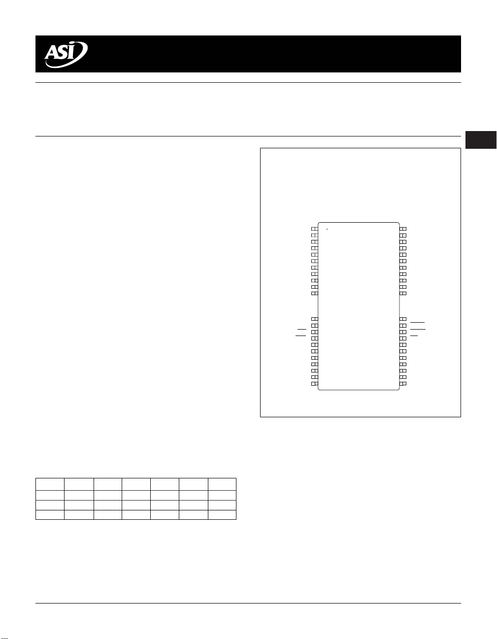
PIN ASSIGNMENT (Top View)
44/50-Pin SOJ/LCC/Gull Wing
450mil
1
Vcc
2
DQ1
3
DQ2
4
DQ3
5
DQ4
6
Vcc
7
DQ5
8
DQ6
9
DQ7
10
DQ8
11
NC
15
NC
16
NC
17
WE
18
RAS
19
NC
20
NC
21
A0
22
A1
23
A2
24
A3
25
Vcc
an internal ?C?A/S.
The AS4LC1M16 ?C?A/S function and timing are determined by the first ?C?A/S (?C?A?S/L or ?C?A?S?H) to transition LOW
and the last ?C?A/S to transition back HIGH. Use of only one
of the two results in a BYTE WRITE cycle. ?C?A?S/L transitioning
LOW selects an access cycle for the lower byte (DQ1-DQ8)
and ?C?A?S?H transitioning LOW selects an access cycle for the
upper byte (DQ9-DQ16).
Each bit is uniquely addressed through the 20 address bits
during READ or WRITE cycles. These are entered 10 bits
(A0-A9) at a time. ?R?A/S is used to latch the first 10 bits and
?C?A/S the latter 10 bits. The ?C?A/S function also determines
whether the cycle will be a refresh cycle (?R?A/S ONLY) or an
active cycle (READ, WRITE or READ WRITE) once ?R?A/S
goes LOW.
Vss
50
DQ16
49
DQ15
48
DQ14
47
DQ13
46
Vss
45
DQ12
44
DQ11
43
DQ10
42
DQ9
41
NC
40
NC
36
CASL
35
CASH
34
OE
33
A9
32
A8
31
A7
30
A6
29
A5
28
A4
27
Vss
26
AS4LC1M16 Austin Semiconductor, Inc., reserves the right to change products or specifications without notice.
REV. 3/97
DS000020
2-93
Page 2

AUSTIN SEMICONDUCTOR, INC.
,
,,
,,
,,,
,,
GENERAL DESCRIPTION (continued)
The ?C?A/S/L and ?C?A/S?H inputs internally generate a ?C?A/S
signal functioning in a similar manner to the single
?C?A/S input of other DRAMs. The key difference is each
?C?A/S input ( ?C?A/S/L and ?C?A/S?H ) controls its corresponding
8 DQ inputs during WRITE accesses. ?C?A/S/L controls DQ1
through DQ8 and ?C?A/S?H controls DQ9 through DQ16. The
two ?C?A/S controls give the MT4LC1M16E5(S) both BYTE
READ and BYTE WRITE cycle capabilities.
A logic HIGH on ?W/E dictates READ mode while a logic
LOW on ?W/E dictates WRITE mode. During a WRITE cycle,
data-in (D) is latched by the falling edge of WE or ?C?A/S
(?C?A/S/L or ?C?A/S/H), whichever occurs last. An EARLY WRITE
occurs when WE is taken LOW prior to either ?C?A/S falling.
A LATE WRITE or READ-MODIFY-WRITE occurs when
WE falls after ?C?A/S (?C?A/S/L or ?C?A/S/H) was taken LOW.
During EARLY WRITE cycles, the data-outputs (Q) will
remain High-Z regardless of the state of ?O/E. During LATE
WRITE or READ-MODIFY-WRITE cycles, ?O/E must be
taken HIGH to disable the data-outputs prior to applying
input data. If a LATE WRITE or READ-MODIFY-WRITE is
attempted while keeping ?O/E LOW, no write will occur, and
the data-outputs will drive read data from the accessed
location.
The 16 data inputs and 16 data outputs are routed through
16 pins using common I/O. Pin direction is controlled by
?O/E and ?W/E.
AS4LC1M16 883C
1 MEG x 16 DRAM
PRELIMINARY
PAGE ACCESS
PAGE operations allow faster data operations (READ,
WRITE or READ-MODIFY-WRITE) within a row-addressdefined page boundary. The PAGE cycle is always initiated
with a row -address strobed-in by ?R?A/S followed by a column-address strobed-in by ?C?A/S. ?C?A/S may be toggled-in
by holding ?R?A/S LOW and strobing-in different columnaddresses, thus executing faster memory cycles. Returning
?R?A/S HIGH terminates the PAGE MODE of operation.
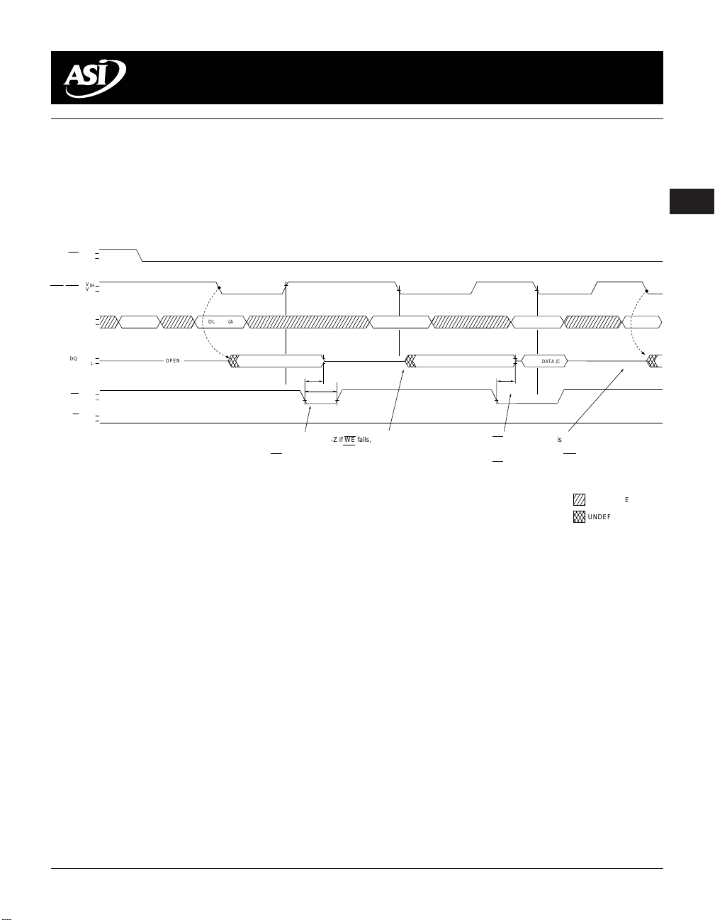
EDO PAGE MODE
The AS4LC1M16 provides EDO PAGE MODE which is
an accelerated FAST PAGE MODE cycle. The primary
advantage of EDO is the availability of data-out even after
?C?A/S returns HIGH. EDO provides for ?C?A/S precharge time
t
CP) to occur without the output data going invalid. This
(
elimination of ?C?A/S output control provides for pipeline
READs.
FAST-PAGE-MODE DRAMs have traditionally turned
the output buffers off (High-Z) with the rising edge of
?C?A /S. EDO-PAGE-MODE DRAMs operate similar to
FAST-PAGE-MODE DRAMs, except data will remain valid
or become valid after ?C?A/S goes HIGH during READs,
provided ?R?A/S and ?O/E are held LOW. If ?O/E is pulsed while
?R?A/S and ?C?A/S are LOW, data will toggle from valid data to
High-Z and back to the same valid data. If ?O/E is toggled or
pulsed after ?C?A/S goes HIGH while ?R?A/S remains LOW, data
will transition to and remain High-Z (refer to Figure 1).
RAS
CASL/CASH
ADDR
DQ
AS4LC1M16 Austin Semiconductor, Inc., reserves the right to change products or specifications without notice.
REV. 3/97
DS000020
V
IH
V
IL
V
IH
V
IL
V
IH
V
IL
V
IOH
V
IOL
V
IH
OE
V
IL
ROW
OPEN
COLUMN (A)
VALID DATA (A)
t
OD
t
OES
The DQs go back to
Low-Z if
t
OE
t
OES is met.
COLUMN (B)
VALID DATA (A)
VALID DATA (B)
t
OD
t
OEHC
The DQs remain High-Z
until the next CAS cycle
t
OEHC is met.
if
COLUMN (C)
VALID DATA (C)
t
OEP
The DQs remain High-Z
until the next CAS cycle
t
OEP is met.
if
COLUMN (D)
t
OD
VALID DATA (D)
DON’T CARE
UNDEFINED
Figure 1
OUTPUT ENABLE AND DISABLE
2-94
Page 3
AUSTIN SEMICONDUCTOR, INC.
,
,
,
,,,
EDO PAGE MODE (continued)
?W/E can also perform the function of disabling the output
drivers under certain conditions, as shown in Figure 2.
During an application, if the DQ outputs are wire OR’d,
?O/E must be used to disable idle banks of DRAMs. Alterna-
V
IH
RAS
V
IL
V
IH
CASL/CASH
V
IL
V
ADDR
IH
V
IL
V
IOH
DQ
V
IOL
V
IH
WE
V
IL
V
IH
OE
V
IL
ROW
OPEN
COLUMN (A)
VALID DATA (A)
t
WHZ
t
WPZ
The DQs go to High-Z if WE falls, and if tWPZ is met,
will remain High-Z until CAS goes LOW with
WE HIGH (i.e., until a READ cycle is initiated).
AS4LC1M16 883C
1 MEG x 16 DRAM
PRELIMINARY
tively, pulsing ?W/E to the idle banks during ?C?A/S HIGH time
will also High-Z the outputs. Independent of ?O/E control,
the outputs will disable after
from the rising edge of ?R?A/S or ?C?A/S, whichever occurs last.
COLUMN (B)
VALID DATA (B)
t
OFF, which is referenced
COLUMN (C)
INPUT DATA (C)
t
WHZ
WE may be used to disable the DQs to prepare
for input data in an EARLY WRITE cycle. The DQs
will remain High-Z until CAS goes LOW with
WE HIGH (i.e., until a READ cycle is initiated).
COLUMN (D)
Figure 2
??
//
?W
/E CONTROL OF DQs
??
//
AS4LC1M16 Austin Semiconductor, Inc., reserves the right to change products or specifications without notice.
REV. 3/97
DS000020
2-95
DON’T CARE
UNDEFINED
Page 4
AUSTIN SEMICONDUCTOR, INC.
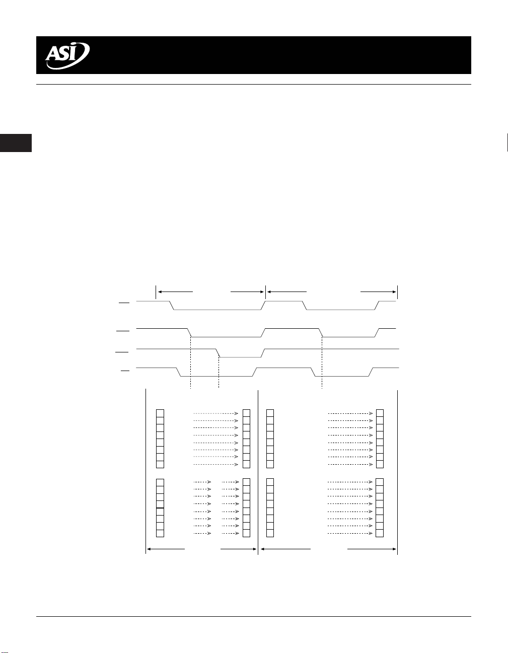
BYTE ACCESS CYCLE
The BYTE WRITEs and BYTE READs are determined by
the use of ?C?A/S/L and ?C?A/S?H. Enabling ?C?A/S/L will select a
lower BYTE access (DQ1-DQ8). Enabling ?C?A/S?H will select
an upper BYTE access (DQ9-DQ16). Enabling both ?C?A/S/L
and ?C?A/S?H selects a WORD WRITE cycle.
The AS4LC1M16 may be viewed as two 1 Meg x 8
DRAMs that have common input controls, with the exception of the / ?C?A/S inputs. Figure 3 illustrates the BYTE WRITE
and WORD WRITE cycles.
Additionally, both bytes must always be of the same
mode of operation if both bytes are active. A ?C?A/S precharge
must be satisfied prior to changing modes of operation
between the upper and lower bytes. For example, an EARLY
WORD WRITE LOWER BYTE WRITE
RAS
CASL
AS4LC1M16 883C
1 MEG x 16 DRAM
PRELIMINARY
WRITE on one byte and a LATE WRITE on the other byte is
not allowed during the same cycle. However, an EARLY
WRITE on one byte and, after a ?C?A/S precharge has been
satisfied, a LATE WRITE on the other byte is permissable.
REFRESH
Preserve correct memory cell data by maintaining power
and executing a ?R?A/S cycle (READ, WRITE) or ?R?A/S refresh
cycle (?R?A/S ONLY, CBR, or HIDDEN) so that all 1,024
combinations of ?R?A/S addresses are executed at least every
16ms, regardless of sequence. The CBR REFRESH cycle will
invoke the refresh counter for automatic ?R?A/S addressing.
CASH
WE
STORED
LOWER BYTE
(DQ1-DQ8)
OF WORD
UPPER BYTE
(DQ9-DQ16)
OF WORD
INPUT
DATA
0
0
1
0
0
0
0
0
X
X
X
X
X
X
X
X
INPUT
DATA
1
0
1
0
1
1
1
1
DATA
1
1
0
1
1
1
1
1
0
1
0
1
0
0
0
0
X = NOT EFFECTIVE (DON'T CARE)
STORED
DATA
0
0
1
0
0
0
0
0
1
0
1
0
1
1
1
1
STORED
DATA
0
0
1
0
0
0
0
0
1
0
1
0
1
1
1
1
INPUT
DATA
1
1
0
1
1
1
1
1
X
X
X
X
X
X
X
X
ADDRESS 1ADDRESS 0
INPUT
DATA
STORED
DATA
1
1
0
1
1
1
1
1
1
0
1
0
1
1
1
1
Figure 3
WORD AND BYTE WRITE EXAMPLE
AS4LC1M16 Austin Semiconductor, Inc., reserves the right to change products or specifications without notice.
REV. 3/97
DS000020
2-96
Page 5
AUSTIN SEMICONDUCTOR, INC.
AS4LC1M16 883C
1 MEG x 16 DRAM
PRELIMINARY
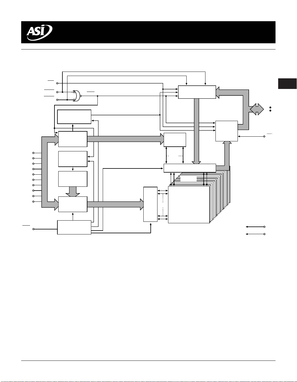
FUNCTIONAL BLOCK DIAGRAM
WE
CASL
CASH
NO. 2 CLOCK
GENERATOR
COLUMNADDRESS
10
BUFFER
A0
A1
A2
A3
A4
A5
A6
A7
A8
A9
CONTROLLER
10
BUFFERS (10)
REFRESH
REFRESH
COUNTER
ROW-
ADDRESS
CAS
10
10
10
ROW
DECODER
1024
DATA-IN BUFFER
COLUMN
DECODER
1024
SENSE AMPLIFIERS
I/O GATING
1024 x 16
1024 x 1024 x 16
MEMORY
ARRAY
DQ1
16
DQ16
DATA-OUT
BUFFER
16
16
OE
RAS
AS4LC1M16 Austin Semiconductor, Inc., reserves the right to change products or specifications without notice.
REV. 3/97
DS000020
NO. 1 CLOCK
GENERATOR
2-97
Vcc
Vss
Page 6

AUSTIN SEMICONDUCTOR, INC.
AS4LC1M16 883C
1 MEG x 16 DRAM
PRELIMINARY
TRUTH TABLE
ADDRESSES
t
FUNCTION ?R?A/S ?C?A/S/L ?C?A/S/H ?W/E ?O/E
Standby H H>XH>X X X X X High-Z
READ: WORD L L L H L ROW COL Data-Out
READ: LOWER BYTE L L H H L ROW COL Lower Byte,
READ: UPPER BYTE L H L H L ROW COL Lower Byte, Data-Out
WRITE: WORD L L L L X ROW COL Data-In
(EARLY WRITE)
WRITE: LOWER L L H L X ROW COL Lower Byte, Data-In
BYTE (EARLY) Upper Byte, High-Z
WRITE: UPPER L H L L X ROW COL Lower Byte, High-Z
BYTE (EARLY) Upper Byte, Data-In
READ WRITE L L L H>LL>H ROW COL Data-Out, Data-In 1, 2
EDO-PAGE-MODE 1st Cycle L H>LH>L H L ROW COL Data-Out 2
READ 2nd Cycle L H>LH>L H L n/a COL Data-Out 2
Any Cycle L L>HL>H H L n/a n/a Data-Out 2
EDO-PAGE-MODE 1st Cycle L H>LH>L L X ROW COL Data-In 1
WRITE 2nd Cycle L H>LH>L L X n/a COL Data-In 1
EDO-PAGE-MODE 1st Cycle L H>LH>LH>LL>H ROW COL Data-Out, Data-In 1, 2
READ-WRITE 2nd Cycle L H>LH>LH>LL>H n/a COL Data-Out, Data-In 1, 2
HIDDEN READ L>H>L L L H L ROW COL Data-Out 2
REFRESH WRITE L>H>L L L L X ROW COL Data-In 1, 3
?R?A/S-ONLY REFRESH L H H X X ROW n/a High-Z
CBR REFRESH H>L L L H X X X High-Z 4
t
R
C DQs NOTES
Upper Byte, Data-Out
Upper Byte
NOTE: 1. These WRITE cycles may also be BYTE WRITE cycles (either ?C?A/S/L or ?C?A/S/H active).
AS4LC1M16 Austin Semiconductor, Inc., reserves the right to change products or specifications without notice.
REV. 3/97
DS000020
2. These READ cycles may also be BYTE READ cycles (either ?C?A/S/L or ?C?A/S/H active).
3. EARLY WRITE only.
4. Only one ?C?A/S must be active (?C?A/S/L or ?C?A/S/H).
2-98
Page 7
AUSTIN SEMICONDUCTOR, INC.
AS4LC1M16 883C
1 MEG x 16 DRAM
PRELIMINARY
ABSOLUTE MAXIMUM RATINGS*
Voltage on VCC pin Relative to VSS .............. -1.0V to +4.6V
Voltage on NC, Inputs or I/O pins
Relative to Vss ................................................. -1.0V to +5.5V
Operating Temperature, T
...................................................................... T
Storage Temperature................................... -55°C to +150°C
(ambient) ..... TA(MIN)=-55°C
A
(MAX)=125°C
C
Power Dissipation ............................................................. 1W
Short Circuit Output Current ..................................... 50mA
ELECTRICAL CHARACTERISTICS AND RECOMMENDED DC OPERATING CONDITIONS
(Notes: 1, 2, 3) (VCC = +3.3V ±0.3V)
PARAMETER/CONDITION SYMBOL MIN MAX UNITS NOTES
Supply Voltage VCC 3.0 3.6 V
Input High (Logic 1) Voltage, all inputs (including NC pins) VIH 2.0 VCC+1 V
Input Low (Logic 0) Voltage, all inputs (including NC pins) VIL -1.0 0.8 V
INPUT LEAKAGE CURRENT
Any input 0V ≤ VIN ≤ 5.5V VCC = 3.6V II -2 2 µA4
(All other pins not under test = 0V)
OUTPUT LEAKAGE CURRENT (Q is disabled; 0V ≤ VOUT ≤ 5.5V) VCC=3.6V IOZ -10 10 µA
OUTPUT LEVELS V
Output High Voltage (I
Output Low Voltage (I
OUT = -2.0mA)
OUT = 2.0mA) VOL 0.4 V
*Stresses greater than those listed under “Absolute Maximum Ratings” may cause permanent damage to the device.
This is a stress rating only and functional operation of the
device at these or any other conditions above those indicated in the operational sections of this specification is not
implied. Exposure to absolute maximum rating conditions
for extended periods may affect reliability.
OH 2.4 V
MAX
PARAMETER/CONDITION SYMBOL -6 -7 -8 UNITS NOTES
STANDBY CURRENT: (TTL) (?R?A/S = ?C?A/S = VIH)ICC1 22 2mA
STANDBY CURRENT: (CMOS) I
CC2 11 1mA
(?R?A/S = ?C?A/S = other inputs = VCC -0.2V)
OPERATING CURRENT: Random READ/WRITE
Average power supply current I
CC3 170 155 140 mA 5, 6
(?R?A/S, ?C?A/S address cycling: tRC = tRC [MIN])
OPERATING CURRENT: EDO PAGE MODE
Average power supply current I
CC4 130 120 110 mA 5, 6
(?R?A/S = VIL, ?C?A/S, address cycling: tPC = tPC [MIN])
REFRESH CURRENT: ?R?A/S ONLY
Average power supply current I
CC5 160 145 130 mA 5, 6
(?R?A/S cycling, ?C?A/S=VIH: tRC = tRC [MIN])
REFRESH CURRENT: CBR
Average power supply current I
CC6 150 140 130 mA 5, 7
(?R?A/S, ?C?A/S address cycling: tRC = tRC [MIN])
AS4LC1M16 Austin Semiconductor, Inc., reserves the right to change products or specifications without notice.
REV. 3/97
DS000020
2-99
Page 8

AUSTIN SEMICONDUCTOR, INC.
AS4LC1M16 883C
1 MEG x 16 DRAM
PRELIMINARY
CAPACITANCE
PARAMETER SYMBOL MAX UNITS NOTES
Input Capacitance: Addresses CI1 7pF8
Input Capacitance: ?R?A/S, ?C?A/S/L,?C?A/S/H, ?W/E, ?O/ECI27pF8
Input/Output Capacitance: DQ C
ELECTRICAL CHARACTERISTICS AND RECOMMENDED AC OPERATING CONDITIONS
(Notes: 2, 3, 6, 9, 10, 11, 12,) (VCC = +3.3V ±0.3V)
AC CHARACTERISTICS -6 -7 -8
PARAMETER SYM MIN MAX MIN MAX MIN MAX UNITS NOTES
Access time from column-address
Column-address set-up to ?C?A/S precharge
Column-address hold time (referenced to ?R?A/S)
Column-address setup time
Row-address setup time
Column-address to ?W/E delay time
Access time from ?C?A/S
Column-address hold time
?C?A/S pulse width
?C?A/S hold time (CBR REFRESH)
Last ?C?A/S going LOW to first ?C?A/S to return HIGH
?C?A/S to output in Low-Z
Data output hold after next ?C?A/S LOW
?C?A/S precharge time
Access time from ?C?A/S precharge
?C?A/S to ?R?A/S precharge time
?C?A/S hold time
?C?A/S setup time (CBR REFRESH)
?C?A/S to ?W/E delay time
Write command to ?C?A/S lead time
Data-in hold time
Data-in hold time (referenced to ?R?A/S)
Data-in setup time
Output disable
Output Enable
?O/E hold time from ?W/E during READ-MODIFY-WRITE cycletOEH 12 12 15 ns 18
?O/E HIGH hold from ?C?A/S HIGH
?O/E HIGH pulse width
t
AA 30 35 40 ns
t
ACH 15 15 25 ns
t
AR 45 50 60 ns
t
ASC 0 0 0 ns 25
t
ASR 0 0 0 ns 25
t
AWD 55 60 65 ns 13
t
CAC 15 20 20 ns 14, 26
t
CAH 10 12 15 ns 25
t
CAS 12 10,000 13 10,000 15 10,000 ns 27
t
CHR 10 12 15 ns 7, 28
t
CLCH 10 10 15 ns 29
t
CLZ 0 0 0 ns 26
t
COH 3 3 3 ns
t
CP 10 10 10 ns 15, 30
t
CPA 35 40 40 ns 26
t
CRP 5 5 5 ns 28
t
CSH 50 55 60 ns 28
t
CSR 5 5 10 ns 7, 25
t
CWD 35 40 45 ns 13, 25
t
CWL 15 15 20 ns 28
t
DH 10 12 15 ns 16, 2 6
t
DHR 45 55 60 ns
t
DS 0 0 0 ns 16, 26
t
OD 0 15 0 15 0 15 ns
t
OE 15 20 20 ns 17, 26
t
OEHC 10 10 10 ns 18
t
OEP 10 10 10 ns
IO 8pF8
AS4LC1M16 Austin Semiconductor, Inc., reserves the right to change products or specifications without notice.
REV. 3/97
DS000020
2-100
Page 9

AUSTIN SEMICONDUCTOR, INC.
AS4LC1M16 883C
1 MEG x 16 DRAM
PRELIMINARY
ELECTRICAL CHARACTERISTICS AND RECOMMENDED AC OPERATING CONDITIONS
(Notes: 2, 3, 6, 9, 10, 11, 12, 20) (VCC = +3.3V ±0.3V)
AC CHARACTERISTICS -6 -7 -8
PARAMETER SYM MIN MAX MIN MAX MIN MAX UNITS NOTES
?O/E LOW to ?C?A/S HIGH setup time
Output buffer turn-off delay
?O/E setup prior to ?R?A/S during HIDDEN REFRESH cycletORD 0 0 0 ns
EDO-PAGE-MODE READ or WRITE cycle time
EDO-PAGE-MODE READ-WRITE cycle time
Access time from ?R?A/S
?R?A/S to column-address delay time
Row-address hold time
Column-address to ?R?A/S lead time
?R?A/S pulse width
?R?A/S pulse width (EDO PAGE MODE)
Random READ or WRITE cycle time
?R?A/S to ?C?A/S delay time
Read command hold time (referenced to ?C?A/S)
Read command setup time
Refresh period (1,024 cycles)
?R?A/S precharge time
?R?A/S to ?C?A/S precharge time
Read command hold time (referenced to ?R?A/S)
?R?A/S hold time
READ WRITE cycle time
?R?A/S to ?W/E delay time
Write command to ?R?A/S lead time
Transition time (rise or fall)
Write command hold time
Write command hold time (referenced to ?R?A/S)
?W/E command setup time
Output disable delay from ?W/E
Write command pulse width
?W/E pulse width to disable at ?C?A/S HIGH
?W/E hold time (CBR REFRESH)
?W/E setup time (CBR REFRESH)
t
OES 5 5 10 ns
t
OFF 0 15 0 15 0 20 ns 20, 26
t
PC 30 35 40 ns 31
t
PRWC 75 85 90 ns 31
t
RAC 60 70 80 ns 19
t
RAD 12 30 12 35 15 40 ns 21
t
RAH 10 10 10 ns
t
RAL 30 35 40 ns
t
RAS 60 10,000 70 10,000 80 10,000 ns
t
RASP 60 100,000 70 100,000 80 100,000 ns
t
RC 110 130 150 ns
t
RCD 14 45 14 50 16 60 ns 22, 25
t
RCH 0 0 0 ns 23, 28
t
RCS 0 0 0 ns 25
t
REF 16 16 16 ms
t
RP 40 50 60 ns
t
RPC 5 5 5 ns
t
RRH 0 0 0 ns 23
t
RSH 13 15 20 ns 32
t
RWC 150 180 200 ns
t
RWD 80 90 105 ns 13
t
RWL 15 18 20 ns
t
T 2 50 2 50 2 50 ns
t
WCH 10 12 15 ns 32
t
WCR 45 55 60 ns
t
WCS 0 0 0 ns 13, 25
t
WHZ 0 13 0 15 0 20 ns
t
WP 10 12 15 ns
t
WPZ 10 12 15 ns
t
WRH 10 10 10 ns
t
WRP 10 10 10 ns
AS4LC1M16 Austin Semiconductor, Inc., reserves the right to change products or specifications without notice.
REV. 3/97
DS000020
2-101
Page 10

AUSTIN SEMICONDUCTOR, INC.
NOTES
1. All voltages referenced to VSS.
2. The minimum specifications are used only to indicate
cycle time at which proper operation over the full
temperature range (0˚C ≤ T
3. An initial pause of 100µs is required after power-up
followed by eight ?R?A/S refresh cycles (?R?A/S ONLY or
CBR with ?W/E HIGH) before proper device operation
is assured. The eight ?R?A/S cycle wake-ups should be
repeated any time the
exceeded.
4. NC pins are assumed to be left floating and are not
tested for leakage.
CC is dependent on output loading and cycle rates.
5. I
Specified values are obtained with minimum cycle
time and the outputs open.
6. Column address changed once each cycle.
7. Enables on-chip refresh and address counters.
8. This parameter is sampled. V
9. AC characteristics assume
IH (MIN) and VIL (MAX) are reference levels for
10. V
measuring timing of input signals. Transition times
are measured between V
and VIH).
11. In addition to meeting the transition rate specification, all input signals must transit between V
IL (or between VIL and VIH) in a monotonic manner.
V
12. Measured with a load equivalent to two TTL gates,
100pF and V
t
WCS, tRWD, tAWD and tCWD are not restrictive
13.
operating parameters.
WRITE cycles.
OL = 0.8V and VOH = 2.0V.
t
RWD, tAWD and tCWD apply to
READ-MODIFY-WRITE cycles. If
(MIN), the cycle is an EARLY WRITE cycle and the
data output will remain an open circuit throughout
the entire cycle. If
t
RWD (MIN), tAWD ≥ tAWD (MIN) and tCWD ≥
t
CWD (MIN), the cycle is a READ-MODIFY-WRITE
t
WCS < tWCS (MIN) and tRWD ≥
and the data output will contain data read from the
selected cell. If neither of the above conditions is met,
the state of data-out is indeterminate. ?O/E held HIGH
and ?W/E taken LOW after ?C?A/S goes LOW results in a
LATE WRITE (?O/E-controlled) cycle.
t
CWD and tAWD are not applicable in a LATE
WRITE cycle.
14. Assumes that
t
RCD ≥ tRCD (MAX).
15. If ?C?A/S is LOW at the falling edge of ?R?A/S, Q will be
maintained from the previous cycle. To initiate a new
cycle and clear the data-out buffer, ?C?A/S must be
pulsed HIGH for
t
CP.
16. These parameters are referenced to ?C?A/S leading edge
in EARLY WRITE cycles and ?W/E leading edge in
LATE WRITE or READ-MODIFY-WRITE cycles.
A ≤ 70˚C) is assured.
t
REF refresh requirement is
CC = +3.0V; f = 1 MHz.
t
T = 2.5ns.
IH and VIL (or between VIL
IH and
t
WCS applies to EARLY
t
WCS ≥ tWCS
t
WCS, tRWD,
AS4LC1M16 883C
1 MEG x 16 DRAM
PRELIMINARY
17. If ?O/E is tied permanently LOW, LATE WRITE or
READ-MODIFY-WRITE operations are not permissible and should not be attempted. Additionally, ?W/E
must be pulsed during ?C?A/S HIGH time in order to
place I/O buffers in High-Z.
18. LATE WRITE and READ-MODIFY-WRITE cycles
must have both
WRITE cycle) in order to ensure that the output
buffers will be open during the WRITE cycle. The
DQs will provide the previously read data if ?C?A/S
remains LOW and ?O/E is taken back LOW after
is met. If ?C?A/S goes HIGH prior to ?O/E going back
LOW, the DQs will remain open.
19. Assumes that
than the maximum recommended value shown in this
t
RAC will increase by the amount that tRCD
table,
exceeds the value shown.
t
OFF (MAX) defines the time at which the output
20.
achieves the open circuit condition, and is not
referenced to V
rising edge of ?R?A/S or ?C?A/S, whichever occurs last.
21. Operation within the
t
RAC (MIN) and tCAC (MIN) can be met. tRAD
(MAX) is specified as a reference point only; if
is greater than the specified
access time is controlled exclusively by
t
RCD is not exceeded.
22. Operation within the
t
RAC (MAX) can be met. tRCD (MAX) is specified as
a reference point only; if
specified
controlled exclusively by
exceeded.
t
23. Either
RCH or tRRH must be satisfied for a READ
cycle.
24. The first ?C?A/Sx edge to transition LOW.
25. Output parameter (DQx) is referenced to corresponding ?C?A/S input; DQ1-DQ8 by ?C?A/S/L and DQ9-DQ16
by ?C?A/S?H.
26. Each ?C?A/Sx must meet minimum pulse width.
27. The last ?C?A/Sx edge to transition HIGH.
28. Last falling ?C?A/Sx edge to first rising ?C?A/Sx edge.
29. Last rising ?C?A/Sx edge to first falling ?C?A/Sx edge.
30. Last rising ?C?A/Sx edge to next cycle’s last rising ?C?A/Sx
edge.
31. Last ?C?A/Sx to go LOW.
32. A HIDDEN REFRESH may also be performed after a
WRITE cycle. In this case, ?W/E = LOW and
?O/E = HIGH.
t
OD and tOEH met (?O/E HIGH during
t
RCD < tRCD (MAX). If tRCD is greater
OH or VOL. It is referenced from the
t
RAD (MAX) limit ensures that
t
RAD (MAX) limit, then
t
RCD (MAX) limit ensures that
t
t
RCD (MAX) limit, then access time is
RCD is greater than the
t
CAC, provided tRAD is not
t
AA, provided
t
OEH
t
RAD
AS4LC1M16 Austin Semiconductor, Inc., reserves the right to change products or specifications without notice.
REV. 3/97
DS000020
2-102
Page 11

AUSTIN SEMICONDUCTOR, INC.
,
,,
,,,
,
,,,,
,,,
,,,
READ CYCLE
t
RC
t
RAS
V
IH
V
RAS
IL
t
RCS
t
t
t
RCD
AR
ASC
CASL/CASH
ADDRVV
WE
DQ
OEVV
t
CRP
V
IH
V
IL
t
RAD
ROW
t
WRPtWRH
NOTE 1
t
RAH
OPEN
t
ASR
IH
IL
V
IH
V
IL
V
OH
V
OL
IH
IL
COLUMN
t
t
t
t
t
t
t
t
t
t
CSH
RSH
CAS
RAL
CAH
ACH
AA
RAC
CAC
CLZ
AS4LC1M16 883C
1 MEG x 16 DRAM
PRELIMINARY
t
RP
t
VALID DATA
t
t
OD
OFF
RRH
t
RCH
NOTE 2
ROW
OPEN
t
CLCH
t
OE
DON’T CARE
UNDEFINED
NOTE: 1. Although ?W/E is a “don’t care” at ?R?A/S time during an access cycle (READ or WRITE), the system designer should implement
?W/E HIGH for
t
OFF is referenced from rising edge of ?R?A/S or ?C?A/S, whichever occurs last.
2.
t
WRP and tWRH. This design implementation will facilitate compatibility with future EDO DRAMs.
TIMING PARAMETERS
-6 -7 -8
SYM MIN MAX MIN MAX MIN MAX UNITS
t
AA 30 35 40 ns
t
ACH 15 15 20 ns
t
AR 45 50 60 ns
t
ASC 0 0 0 ns
t
ASR 0 0 0 ns
t
CAC 15 20 20 ns
t
CAH 10 12 15 ns
t
CAS 12 10,000 13 10,000 20 10,000 ns
t
CLCH 10 10 10 ns
t
CLZ 0 0 0 ns
t
CRP 5 5 5 ns
t
CSH 50 55 60 ns
t
OD 0 15 0 15 0 20 ns
t
OE 15 20 20 ns
t
OFF 0 15 0 15 0 20 ns
AS4LC1M16 Austin Semiconductor, Inc., reserves the right to change products or specifications without notice.
REV. 3/97
DS000020
SYM MIN MAX MIN MAX MIN MAX UNITS
t
RAC 60 70 80 ns
t
RAD 12 30 12 35 15 40 ns
t
RAH 10 10 10 ns
t
RAL 30 35 40 ns
t
RAS 60 10,000 70 10,000 80 10,000 ns
t
RC 110 130 150 ns
t
RCD 14 45 14 50 20 60 ns
t
RCH 0 0 0 ns
t
RCS 0 0 0 ns
t
RP 40 50 60 ns
t
RRH 0 0 0 ns
t
RSH 13 15 15 ns
t
WRH 10 10 10 ns
t
WRP 10 10 10 ns
2-103
-6 -7 -8
Page 12

AUSTIN SEMICONDUCTOR, INC.
,,
,,,
,,
,
,
,,,
,,,
,,,
,,
,,,
,,,
,,,
,,,
,,,
,,,
,,
,,,
,
,,
,
EARLY WRITE CYCLE
V
IH
RAS
V
IL
t
CRP
CASL/CASH
ADDR
V
IH
V
IL
t
RAD
t
WRPtWRH
NOTE 1
t
RAH
t
WCS
t
ASR
V
IH
V
IL
WE
V
IH
V
IL
V
IOH
DQ
V
IOL
V
IH
OE
V
IL
t
t
RCD
t
AR
t
ASC
DS
COLUMNROW
VALID DATA
t
t
t
t
t
t
t
RC
RAS
CSH
RSH
CAS
RAL
CAH
t
CWL
t
RWL
t
WCR
t
WCH
t
WP
t
DHR
t
DH
t
CLCH
t
ACH
AS4LC1M16 883C
1 MEG x 16 DRAM
PRELIMINARY
t
RP
ROW
NOTE: 1. Although ?W/E is a “don’t care” at ?R?A/S time during an access cycle (READ or WRITE), the system designer should implement
TIMING PARAMETERS
SYM MIN MAX MIN MAX MIN MAX UNITS
t
ACH 15 15 20 ns
t
AR 45 50 60 ns
t
ASC 0 0 0 ns
t
ASR 0 0 0 ns
t
CAH 10 12 15 ns
t
CAS 12 10,000 13 10,000 20 10,000 ns
t
CLCH 10 10 10 ns
t
CRP 5 5 5 ns
t
CSH 50 55 60 ns
t
CWL 15 15 20 ns
t
DH 10 12 15 ns
t
DHR 45 55 55 ns
t
DS 0 0 0 ns
t
RAD 12 30 12 35 15 40 ns
AS4LC1M16 Austin Semiconductor, Inc., reserves the right to change products or specifications without notice.
REV. 3/97
DS000020
t
?W/E HIGH for
WRP and tWRH. This design implementation will facilitate compatibility with future EDO DRAMs.
-6 -7 -8
2-104
DON’T CARE
UNDEFINED
-6 -7 -8
SYM MIN MAX MIN MAX MIN MAX UNITS
t
RAH 10 10 10 ns
t
RAL 30 35 40 ns
t
RAS 60 10,000 70 10,000 80 10,000 ns
t
RC 110 130 150 ns
t
RCD 14 45 14 50 20 60 ns
t
RP 40 50 60 ns
t
RSH 13 15 0 ns
t
RWL 15 15 20 ns
t
WCH 10 12 15 ns
t
WCR 45 55 60 ns
t
WCS 0 0 0 ns
t
WP 10 12 15 ns
t
WRH 10 10 10 ns
t
WRP 10 10 10 ns
Page 13

AUSTIN SEMICONDUCTOR, INC.
,,,
,,,,
,,
,,,,
,,,,
,,
,
,,
,,
READ WRITE CYCLE
(LATE WRITE and READ-MODIFY-WRITE cycles)
t
RWC
t
RAS
V
IH
RAS
V
CASL/CASH
ADDR
WE
IL
t
CRP
V
IH
V
IL
t
V
IH
V
IL
V
IH
V
IL
V
IOH
DQ
V
IOL
V
IH
OE
V
IL
ASR
t
NOTE 1
ROW
WRPtWRH
t
RCD
t
AR
t
RAD
t
RAH
t
ASC
t
RCS
t
CSH
t
RSH
t
t
CAS, CLCH
t
RAL
t
CAH
COLUMN ROW
t
RWD
t
CWD
t
AWD
t
AA
t
RAC
t
CAC
t
CLZ
t
OE
VALID D
AS4LC1M16 883C
1 MEG x 16 DRAM
PRELIMINARY
t
RP
t
ACH
t
CWL
t
RWL
t
WP
tDSt
DH
VALID D
OUT
t
OD
IN
t
OEH
OPENOPEN
DON’T CARE
UNDEFINED
NOTE: 1. Although ?W/E is a “don’t care” at ?R?A/S time during an access cycle (READ or WRITE), the system designer should implement
TIMING PARAMETERS
SYM MIN MAX MIN MAX MIN MAX UNITS
t
AA 30 35 40 ns
t
ACH 15 15 20 ns
t
AR 45 50 60 ns
t
ASC 0 0 0 ns
t
ASR 0 0 0 ns
t
AWD 55 60 65 ns
t
CAC 15 20 20 ns
t
CAH 10 12 15 ns
t
CAS 12 10,000 13 10,000 20 10,000 ns
t
CLCH 10 10 10 ns
t
CLZ 0 0 0 ns
t
CRP 5 5 5 ns
t
CSH 50 55 60 ns
t
CWD 35 40 45 ns
t
CWL 15 15 20 ns
t
DH 10 12 15 ns
t
DS 0 0 0 ns
t
OD 0 15 0 15 0 20 ns
AS4LC1M16 Austin Semiconductor, Inc., reserves the right to change products or specifications without notice.
REV. 3/97
DS000020
t
?W/E HIGH for
WRP and tWRH. This design implementation will facilitate compatibility with future EDO DRAMs.
-6 -7 -8
SYM MIN MAX MIN MAX MIN MAX UNITS
t
OE 15 20 20 ns
t
OEH 12 12 15 ns
t
RAC 60 70 80 ns
t
RAD 12 30 12 35 15 40 ns
t
RAH 10 10 10 ns
t
RAL 30 35 40 ns
t
RAS 60 10,000 70 10,000 80 10,000 ns
t
RCD 14 45 14 50 20 60 ns
t
RCS 0 0 0 ns
t
RP 40 50 60 ns
t
RSH 13 15 15 ns
t
RWC 150 180 200 ns
t
RWD 80 90 105 ns
t
RWL 15 15 20 ns
t
WP 10 12 15 ns
t
WRH 10 10 10 ns
t
WRP 10 10 10 ns
2-105
-6 -7 -8
Page 14

,,,
,,
,
RAS
,
CASL/CASH
ADDR
AUSTIN SEMICONDUCTOR, INC.
EDO-PAGE-MODE READ CYCLE
V
IH
V
IL
t
CRP
V
IH
V
IL
t
V
IH
V
IL
V
WE
IH
V
IL
V
OH
DQ
V
OL
V
IH
OE
V
IL
ASR
t
WRPtWRH
NOTE 1
t
CSH
t
t
RAD
RAD
t
RAH
t
t
RCD
t
AR
t
ACH
t
ASC
t
RCS
t
CLZ
tt
CAS, CLCH
t
CAH
t
AA
t
RAC
t
CAC
t
OE
t
OES
t
PC
t
CP
VALID
DATA
AS4LC1M16 883C
1 MEG x 16 DRAM
PRELIMINARY
t
RASP
t
tt
CAS, CLCH
t
ACH
t
t
CAH
ASC
t
AA
t
CPA
t
CAC
t
COH
VALID
DATA
t
CP
t
OEHC
t
t
OD
OD
t
OEP
RSH
t
CAS, CLCH
t
ACH
t
ASC
t
CLZ
t
RAL
t
CAH
COLUMNCOLUMNCOLUMNROW ROW
t
AA
t
CPA
t
CAC
t
OE
t
OES
VALID
DATA
t
RP
t
CP
t
RCH
t
RRH
t
OFF
OPENOPEN
t
OD
DON’T CARE
UNDEFINED
NOTE: 1. Although ?W/E is a “don’t care” at ?R?A/S time during an access cycle (READ or WRITE), the system designer should implement
?W/E HIGH for
t
WRP and tWRH. This design implementation will facilitate compatibility with future EDO DRAMs.
TIMING PARAMETERS
-6 -7 -8
SYM MIN MAX MIN MAX MIN MAX UNITS
t
AA 30 35 40 ns
t
ACH 15 15 20 ns
t
AR 45 50 60 ns
t
ASC 0 0 0 ns
t
ASR 0 0 0 ns
t
CAC 15 20 20 ns
t
CAH 10 12 15 ns
t
CAS 12 10,000 13 10,000 20 10,000 ns
t
CLCH 10 10 10 ns
t
CLZ 0 0 0 ns
t
COH 3 3 5 ns
t
CP 10 10 10 ns
t
CPA 35 40 40 ns
t
CRP 5 5 5 ns
t
CSH 50 55 60 ns
t
OD0 15015020ns
t
OE 15 20 20 ns
t
OEHC 10 10 10 ns
AS4LC1M16 Austin Semiconductor, Inc., reserves the right to change products or specifications without notice.
REV. 3/97
DS000020
SYM MIN MAX MIN MAX MIN MAX UNITS
t
OEP 10 10 10 ns
t
OES 5 5 5 ns
t
OFF3 15315020ns
t
PC 30 35 40 ns
t
RAC 60 70 80 ns
t
RAD 12 30 12 35 15 40 ns
t
RAH 10 10 10 ns
t
RAL 30 35 40 ns
t
RASP 60 100,000 70 100,000 80 100,000 ns
t
RCD 14 45 14 50 20 60 ns
t
RCH 0 0 0 ns
t
RCS 0 0 0 ns
t
RP 40 50 60 ns
t
RRH 0 0 0 ns
t
RSH 13 15 15 ns
t
WRH 10 10 10 ns
t
WRP 10 10 10 ns
2-106
-6 -7 -8
Page 15

,
,
,,,
,,
RAS
,,,
,,,,
,,,,
,,,
,,,
,,,
,,
CASL/CASH
ADDR
AUSTIN SEMICONDUCTOR, INC.
AS4LC1M16 883C
1 MEG x 16 DRAM
PRELIMINARY
EDO-PAGE-MODE EARLY-WRITE CYCLE
t
RASP
V
IH
V
IL
t
CRP
V
IH
V
IL
t
ASR
V
IH
V
IL
t
WRPtWRH
V
IH
WE
V
IL
V
IOH
DQ
V
IOL
V
IH
OE
V
IL
NOTE 1
t
CSH
t
RCD
t
AR
t
RAD
t
RAH
t
WCS
t
ACH
t
ASC
t
DS
t
tt
CAS, CLCH
t
CAH
t
CWL
t
WCH
t
WP
t
WCR
t
DHR
t
DH
VALID DATA VALID DATA VALID DATA
t
PC
t
CP
t
ACH
t
ASC
t
WCS
t
DS
tt
CAS, CLCH
t
CAH
t
CWL
t
WCH
t
WP
t
DH
t
CP
t
RSH
t
CAS, CLCH
t
ACH
t
RAL
t
t
CAH
ASC
COLUMNCOLUMNCOLUMNROW ROW
t
CWL
t
t
WCS
t
DS
WCH
t
WP
t
DH
t
RWL
t
RP
t
CP
DON’T CARE
UNDEFINED
NOTE: 1. Although ?W/E is a “don’t care” at ?R?A/S time during an access cycle (READ or WRITE), the system designer should implement
TIMING PARAMETERS
SYM MIN MAX MIN MAX MIN MAX UNITS
t
ACH 15 15 20 ns
t
AR 45 50 60 ns
t
ASC 0 0 0 ns
t
ASR 0 0 0 ns
t
CAH 10 12 15 ns
t
CAS 12 10,000 13 10,000 20 10,000 ns
t
CLCH 10 10 10 ns
t
CP 10 10 10 ns
t
CRP 5 5 5 ns
t
CSH 50 55 60 ns
t
CWL 15 15 20 ns
t
DH 10 12 15 ns
t
DHR 45 55 55 ns
t
DS 0 0 0 ns
t
PC 25 30 40 ns
AS4LC1M16 Austin Semiconductor, Inc., reserves the right to change products or specifications without notice.
REV. 3/97
DS000020
t
?W/E HIGH for
WRP and tWRH. This design implementation will facilitate compatibility with future EDO DRAMs.
-6 -7 -8
SYM MIN MAX MIN MAX MIN MAX UNITS
t
RAD 12 30 12 35 15 40 ns
t
RAH 10 10 10 ns
t
RAL 30 35 40 ns
t
RASP 60 125,000 70 125,000 80 100,000 ns
t
RCD 14 45 14 50 20 60 ns
t
RP 40 50 60 ns
t
RSH 13 15 15 ns
t
RWL 15 15 20 ns
t
WCH 10 12 15 ns
t
WCR 45 55 60 ns
t
WCS 0 0 0 ns
t
WP 10 12 15 ns
t
WRH 10 10 10 ns
t
WRP 10 10 10 ns
2-107
-6 -7 -8
Page 16

AUSTIN SEMICONDUCTOR, INC.
,,,,
,,
,,
,,
,
,
,,
EDO-PAGE-MODE READ-WRITE CYCLE
(LATE WRITE and READ-MODIFY-WRITE cycles)
t
RASP
t
t
PRWC
PC
t
t
CLCH
WP
t
DH
VALID
D
IN
t
OD
CP
t
ASCtCAH
t
AA
t
CPA
t
CAC
t
CLZ
t
t
CAS,
t
CWL
t
WP
t
AWD
t
CWD
t
DH
t
DS
VALID
D
OUT
OE
CASL/CASH
ADDR
V
IH
RAS
V
IL
t
CRP
V
IH
V
IL
V
IH
V
IL
WE
V
IH
V
IL
V
IOH
DQ
V
IOL
V
IH
OE
V
IL
t
AR
t
RAD
t
ASRtRAH
ROW COLUMN COLUMN COLUMN ROW
t
WRPtWRH
NOTE 2
t
CSH
t
RCD
t
RAC
OPEN
t
CAS,
t
t
ASC
CAH
t
RWD
t
RCS
t
t
t
CWL
t
t
AWD
t
CWD
t
AA
t
DS
CAC
CLZ
VALID
D
OUT
t
OE
AS4LC1M16 883C
1 MEG x 16 DRAM
PRELIMINARY
t
RP
t
CP
t
ASCtCAH
t
AA
t
CPA
CAC
CLZ
t
OE
t
RSH
t
t
CLCH
CAS,
t
RAL
t
AWD
t
CWD
t
DS
VALID
D
OUT
t
CP
t
RWL
t
CWL
t
WP
t
DH
VALID
OPEN
D
IN
t
OD
t
OEH
DON’T CARE
UNDEFINED
NOTE 1
t
CLCH
t
t
VALID
D
IN
t
OD
NOTE: 1.tPC is for LATE WRITE cycles only.
TIMING PARAMETERS
SYM MIN MAX MIN MAX MIN MAX UNITS
t
AA 30 35 40 ns
t
AR 45 50 60 ns
t
ASC 0 0 0 ns
t
ASR 0 0 0 ns
t
AWD 55 60 65 ns
t
CAC 15 20 20 ns
t
CAH 10 12 15 ns
t
CAS 12 10,000 13 10,000 20 10,000 ns
t
CLCH 10 10 10 ns
t
CLZ 0 0 0 ns
t
CP 10 10 10 ns
t
CPA 35 40 40 ns
t
CRP 5 5 5 ns
t
CSH 50 55 60 ns
t
CWD 35 40 45 ns
t
CWL 15 15 20 ns
t
DH 10 12 15 ns
t
DS 0 0 0 ns
t
OD 0 15 0 15 0 20 ns
AS4LC1M16 Austin Semiconductor, Inc., reserves the right to change products or specifications without notice.
REV. 3/97
DS000020
2. Although ?W/E is a “don’t care” at ?R?A/S time during an access cycle (READ or WRITE), the system designer should implement
?W/E HIGH for
-6 -7 -8
t
WRP and tWRH. This design implementation will facilitate compatibility with future EDO DRAMs.
-6 -7 -8
SYM MIN MAX MIN MAX MIN MAX UNITS
t
OE 15 20 20 ns
t
OEH 12 12 15 ns
t
PC 25 30 40 ns
t
PRWC 75 85 90 ns
t
RAC 60 70 80 ns
t
RAD 12 30 12 35 15 40 ns
t
RAH 10 10 10 ns
t
RAL 30 35 40 ns
t
RASP 60 125,000 70 125,000 80 100,000 ns
t
RCD 14 45 14 50 20 60 ns
t
RCS 0 0 0 ns
t
RP 40 50 60 ns
t
RSH 13 15 15 ns
t
RWD 80 90 105 ns
t
RWL 15 15 20 ns
t
WP 10 12 15 ns
t
WRH 10 10 10 ns
t
WRP 10 10 10 ns
2-108
Page 17

RAS
,
,
,,,
,
,,
CASL/CASH
ADDR
DQ
AUSTIN SEMICONDUCTOR, INC.
EDO-PAGE-MODE READ-EARLY-WRITE CYCLE
(Pseudo READ-MODIFY-WRITE)
V
IH
V
IL
t
CRP
V
IH
V
IL
t
RAD
t
ASRtRAH
V
IH
V
IL
V
IH
WE
V
IL
V
IOH
V
IOL
V
IH
OE
V
IL
ROW
t
WRPtWRH
NOTE 1
OPEN
t
CSH
t
RCD
t
AR
t
ASC
COLUMN (A)
t
RCS
t
RAC
t
PC
t
t t
CAS, CLCH
t
CAH
t
AA
t
CAC
t
OE
t
CP
VALID D
t
RASP
t
ASCtCAH
COLUMN (B)
t
CPA
OUT
t
CAS, CLCH
t
RCH
t
AA
t
CAC
t
COH
AS4LC1M16 883C
1 MEG x 16 DRAM
PRELIMINARY
t
RP
tDSt
VALID D
t
RSH
tt
CAS, CLCH
t
RAL
t
ACH
t
WCH
DH
IN
t
CP
ROW
DON’T CARE
UNDEFINED
t
PC
t
CP
t
ASCtCAH
COLUMN (N)
t
WCS
t
WHZ
VALID
D
OUT
NOTE: 1. Although ?W/E is a “don’t care” at ?R?A/S time during an access cycle (READ or WRITE), the system designer should implement
TIMING PARAMETERS
SYM MIN MAX MIN MAX MIN MAX UNITS
t
AA 30 35 40 ns
t
ACH 15 15 20 ns
t
AR 45 50 60 ns
t
ASC 0 0 0 ns
t
ASR 0 0 0 ns
t
CAC 15 20 20 ns
t
CAH 10 12 15 ns
t
CAS 12 10,000 13 10,000 20 10,000 ns
t
CLCH 10 10 10 ns
t
COH 3 3 5 ns
t
CP 10 10 10 ns
t
CPA 35 40 40 ns
t
CRP 5 5 5 ns
t
CSH 50 55 60 ns
t
DH 10 12 15 ns
t
DS 0 0 0 ns
t
OE 15 20 20 ns
AS4LC1M16 Austin Semiconductor, Inc., reserves the right to change products or specifications without notice.
REV. 3/97
DS000020
t
?W/E HIGH for
WRP and tWRH. This design implementation will facilitate compatibility with future EDO DRAMs.
-6 -7 -8
-6 -7 -8
SYM MIN MAX MIN MAX MIN MAX UNITS
t
PC 25 30 40 ns
t
RAC 60 70 80 ns
t
RAD 12 30 12 35 15 40 ns
t
RAH 10 10 10 ns
t
RAL 30 35 40 ns
t
RASP 60 125,000 70 125,000 80 100,000 ns
t
RCD 14 45 14 50 20 60 ns
t
RCH 0 0 0 ns
t
RCS 0 0 0 ns
t
RP 40 50 60 ns
t
RSH 13 15 15 ns
t
WCH 10 12 15 ns
t
WCS 0 0 0 ns
t
WHZ 0 13 0 15 0 20 ns
t
WRH 10 10 10 ns
t
WRP 10 10 10 ns
2-109
Page 18

AUSTIN SEMICONDUCTOR, INC.
,,,
,,,
,
,,,
,,
READ CYCLE
(with ?W/E-controlled disable)
V
IH
RAS
V
IL
t
CRP
V
ADDRVV
WE
DQ
OEVV
IH
V
IL
t
RAD
ROW
t
WRPtWRH
NOTE 1
t
RAH
OPEN
t
ASR
IH
IL
V
IH
V
IL
V
OH
V
OL
IH
IL
CASL/CASH
t
RCS
t
t
t
RCD
AR
ASC
COLUMN
t
CSH
t
t
CAS, CLCH
t
CAH
t
AA
t
RAC
t
CAC
t
CLZ
AS4LC1M16 883C
1 MEG x 16 DRAM
PRELIMINARY
t
CP
t
ASC
COLUMN
t
t
RCH
t
OE
VALID DATA
t
WPZ
RCS
t
WHZ
t
OD
OPEN
t
CLZ
DON’T CARE
UNDEFINED
NOTE: 1. Although ?W/E is a “don’t care” at ?R?A/S time during an access cycle (READ or WRITE), the system designer should implement
?W/E HIGH for
t
WRP and tWRH. This design implementation will facilitate compatibility with future EDO DRAMs.
TIMING PARAMETERS
SYM MIN MAX MIN MAX MIN MAX UNITS
t
AA 30 35 40 ns
t
AR 45 50 60 ns
t
ASC 0 0 0 ns
t
ASR 0 0 0 ns
t
CAC 15 20 20 ns
t
CAH 10 12 15 ns
t
CAS 12 10,000 13 10,000 20 10,000 ns
t
CLCH 10 10 10 ns
t
CLZ 0 0 0 ns
t
CP 10 10 10 ns
t
CRP 5 5 5 ns
t
CSH 50 55 60 ns
AS4LC1M16 Austin Semiconductor, Inc., reserves the right to change products or specifications without notice.
REV. 3/97
DS000020
SYM MIN MAX MIN MAX MIN MAX UNITS
t
OD 0 15 0 15 0 15 ns
t
OE 15 20 20 ns
t
RAC 60 70 80 ns
t
RAD 12 30 12 35 15 40 ns
t
RAH 10 10 10 ns
t
RCD 14 45 14 50 20 60 ns
t
RCH 0 0 0 ns
t
RCS 0 0 0 ns
t
WHZ 0 13 0 15 0 20 ns
t
WPZ 10 12 15 ns
t
WRH 10 10 10 ns
t
WRP 10 10 10 ns
2-110
-6 -7 -8
-6 -7 -8
Page 19

,,,
,,,
,
RAS
,,,
,,,,
,,
,,
,,
,,,
,
,,
CASL/CASH
ADDR
AUSTIN SEMICONDUCTOR, INC.
??
??
//
?R
?A
/S-ONLY REFRESH CYCLE
??
??
//
t
RAS
V
IH
V
IL
V
IH
V
IL
V
IH
V
IL
V
OH
Q
V
OL
V
IH
WE
V
IL
t
CRP
t
ASR
t
WRP
ROW
NOTE 1
t
WRH
t
RAH
CBR REFRESH CYCLE
(Addresses and ?O/E = DON’T CARE)
OPEN
AS4LC1M16 883C
1 MEG x 16 DRAM
PRELIMINARY
t
RC
t
RPC
t
RP
ROW
t
t
WRH
WRP
t
RP
V
IH
RAS
V
IL
V
CASL and CASH
IH
V
IL
V
OH
V
DQ
OL
V
IH
WE
V
IL
NOTE: 1. Although ?W/E is a “don’t care” at ?R?A/S time during an access cycle (READ or WRITE), the system designer should
implement ?W/E HIGH for
t
WRP and tWRH are for system design reference only. The ?W/E signal is actually a “don’t care” at ?R?A/S time during a CBR
2.
t
RPC
t
t
CP
CSR
t
WRP and tWRH. This design implementation will facilitate compatibility with future EDO DRAMs.
t
WRPtWRH
NOTE 2
t
t
RAS
CHR
t
RPC
t
OPEN
RP
t
CSR
t
t
CHR
WRPtWRH
t
RAS
REFRESH. However, ?W/E should be held HIGH at ?R?A/S time during a CBR REFRESH to ensure compatibility with other
DRAMs that require ?W/E HIGH at ?R?A/S time during a CBR REFRESH.
TIMING PARAMETERS
SYM MIN MAX MIN MAX MIN MAX UNITS
-6 -7 -8
t
ASR 0 0 0 ns
t
CHR 10 12 15 ns
t
CP 10 10 10 ns
t
CRP 5 5 5 ns
t
CSR 5 5 10 ns
t
RAH 10 10 10 ns
SYM MIN MAX MIN MAX MIN MAX UNITS
t
RAS 60 10,000 70 10,000 80 10,000 ns
t
RC 105 125 150 ns
t
RP 40 50 60 ns
t
RPC 5 5 5 ns
t
WRH 10 10 10 ns
t
WRP 10 10 10 ns
-6 -7 -8
AS4LC1M16 Austin Semiconductor, Inc., reserves the right to change products or specifications without notice.
REV. 3/97
DS000020
2-111
Page 20

,
,,,
,,,
,,,
,,
RAS
,,,,
,,
CASL/CASH
ADDR
DQx
OE
AUSTIN SEMICONDUCTOR, INC.
HIDDEN REFRESH CYCLE
(?W/E = HIGH; ?O/E = LOW)
t
RC
t
RAS
V
IH
V
IL
V
IH
V
IL
V
IH
V
IL
V
IOH
V
IOL
V
IH
V
IL
t
CRP
t
ASR
t
RAH
t
AR
t
RAD
t
RCD
t
ASC
t
RSH
t
RAL
t
CAH
COLUMNROW
t
AA
t
RAC
t
CAC
t
CLZ
t
t
ORD
AS4LC1M16 883C
1 MEG x 16 DRAM
PRELIMINARY
32
t
RP
OE
t
RAS
t
CHR
t
OFF
OPENVALID DATAOPEN
t
OD
DON’T CARE
UNDEFINED
TIMING PARAMETERS
-6 -7 -8
SYM MIN MAX MIN MAX MIN MAX UNITS
t
AA 30 35 40 ns
t
AR 45 50 60 ns
t
ASC 0 0 0 ns
t
ASR 0 0 0 ns
t
CAC 15 20 20 ns
t
CAH 10 12 15 ns
t
CHR 10 12 15 ns
t
CLZ 0 0 0 ns
t
CRP 5 5 5 ns
t
OD0 150150 20ns
t
OE 15 20 20 ns
AS4LC1M16 Austin Semiconductor, Inc., reserves the right to change products or specifications without notice.
REV. 3/97
DS000020
SYM MIN MAX MIN MAX MIN MAX UNITS
t
OFF 3 15 3 15 3 15 ns
t
ORD 0 0 0 ns
t
RAC 60 70 80 ns
t
RAD 12 30 12 35 15 40 ns
t
RAH 10 10 10 ns
t
RAL 30 35 40 ns
t
RAS 60 10,000 70 10,000 80 10,000 ns
t
RC 105 125 145 ns
t
RCD 14 45 14 50 20 60 ns
t
RP 40 50 60 ns
t
RSH 13 15 15 ns
2-112
-6 -7 -8
Page 21

AUSTIN SEMICONDUCTOR, INC.
ELECTRICAL TEST REQUIREMENTS
AS4LC1M16 883C
1 MEG x 16 DRAM
PRELIMINARY
MIL-STD-883 TEST REQUIREMENTS (per Method 5005, Table I)
INTERIM ELECTRICAL (PRE-BURN-IN) TEST PARAMETERS 2, 8A, 10
(Method 5004)
FINAL ELECTRICAL TEST PARAMETERS 1*, 2, 3, 7*, 8, 9, 10, 11
(Method 5004)
GROUP A TEST REQUIREMENTS 1, 2, 3, 4**, 7, 8, 9, 10, 11
(Method 5005)
GROUP C AND D END-POINT ELECTRICAL PARAMETERS 1, 2, 3, 7, 8, 9, 10, 11
(Method 5005)
* PDA applies to subgroups 1 and 7.
** Subgroup 4 shall be measured only for initial qualification and after process or design changes, which may affect input
or output capacitance.
SUBGROUPS
AS4LC1M16 Austin Semiconductor, Inc., reserves the right to change products or specifications without notice.
REV. 3/97
DS000020
2-113
Page 22

AUSTIN SEMICONDUCTOR, INC.
AS4LC1M16 883C
1 MEG x 16 DRAM
PRELIMINARY
AS4LC1M16 Austin Semiconductor, Inc., reserves the right to change products or specifications without notice.
REV. 3/97
DS000020
2-114
 Loading...