

Page 1
Features
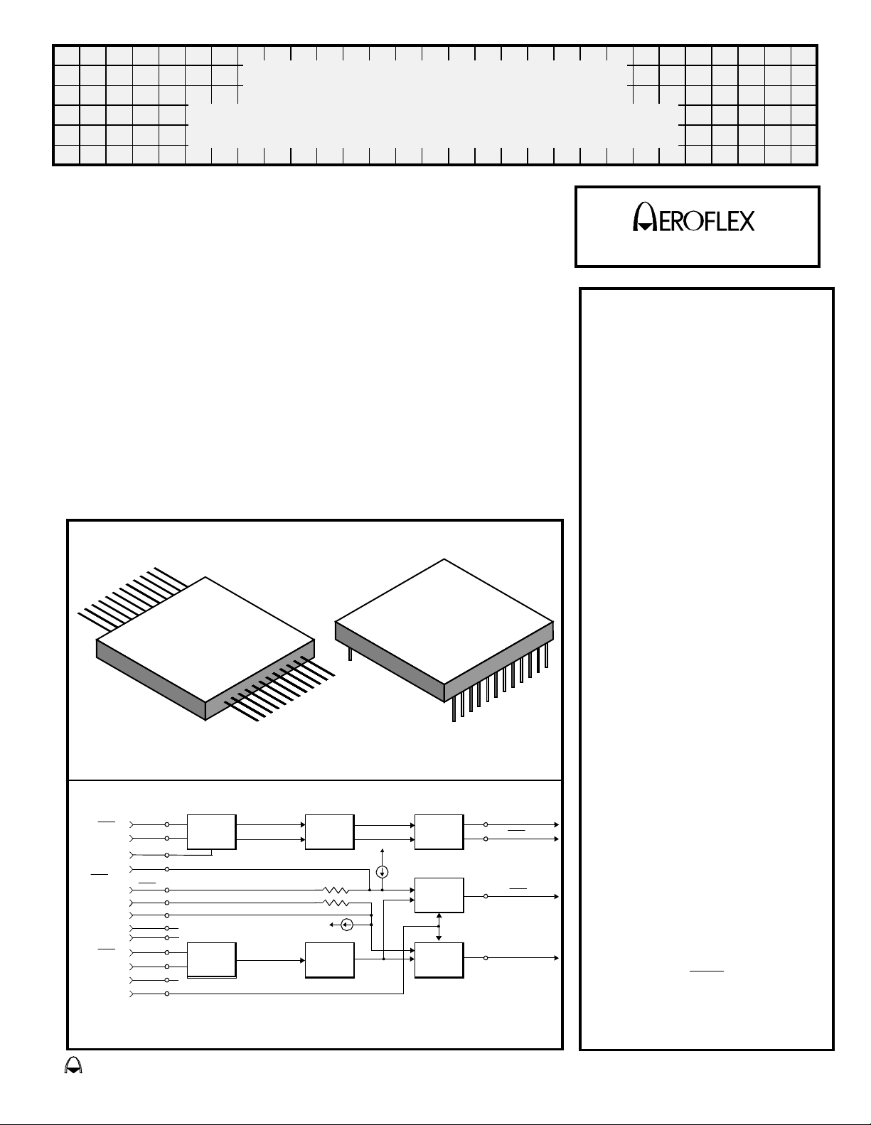
ARX4435N Transceiver
for Macair H009 Spec ificat ion
Preliminary
• ARX4435N transceiver meets Macair H009 data bus
specifications
• Transmitter can be used to drive clock signal line
• Operates with ±15 Volts to ±12 Volts power supplies
• Low power direct replacement for CT1641 and CT1816
devices
• Voltage source output for higher bus drive power
• Plug-in and flat package available
• Monolithic construction using linear ASICs
• Processed and screened to MIL-STD-883 specs
• MIL-PRF-38534 compliant devices available
AEROFLEX
AEROFLEX
ARX 4435NFP
USA-88379
ARX4435NFP / ARX4435N Tran sceiv er s
ARX 4435N
USA-88379
CIRCUIT TECHNOLOGY
www.aeroflex.com
General Description
The Aeroflex Laboratories
Incorporated model ARX4435N and
ARX4435NFP are new generation
monolithic transceivers which
provides compliance with Macair
H009 data bus requirements.
The ARX4435N and ARX4435NFP
perform the front-end analog function
of inputting and outputting data
through a transformer to a H009 data
bus.
Design of these transceivers
reflects particular attention to active
filter performance.This results in low
bit and word error rate with superior
waveform purity and minimal zero
crossover distortion. The ARX4435N
series active filter design has
additional high frequency roll-off to
provide the required low harmonic
distortion waveform without
increasing the delay characteristics
significantly.
Efficient transmitter electrical and
thermal design results in low internal
power dissipation and temperature
rise at high and low duty cycle.
TX DATA IN
TX DATA IN
TX INHIBIT
EXT THRESHOLD
DATA
SET INTERNAL
THRESHOLD
EXT THRESHOLD
DATA
-12V or -15V
RX DATA IN
RX DATA IN
+15V or +12V
STROBE
DATA
DATA
+5 V
eroflex Cir cu it T
DRIVER
INPUT
AMP
+VTH
-VTH
SHAPING
–
~4K
+
~4K
V-
ACTIVE
FILTER
V+
+
–
Block Diagram (without Transformer)
echnology
– Data Bus Modules For The Future © SCD4435N REV A 7/27/00
OUTPUT
STAGE
COMP.
COMP.
TX DATA OUT
TX DATA OUT
RX DATA OUT
RX DATA OUT
Transmitter
The Transmitter section accepts
complement ary TT L data at the input,
and when coupled to the data bus
with a 1:1 transformer, isolated on the
transceiver side with two 35 Ohm
fault isolation resistors, and loaded by
a 170 Ohm ter mination, the data bus
signal produced is 20 Volts nominal
P-P at A-A’. (See Figure 5.) When
both DATA and DATA
low or high, the transmitter output
impedance is low, and signal is
“removed” from the line. In addition,
inputs are held
Page 2
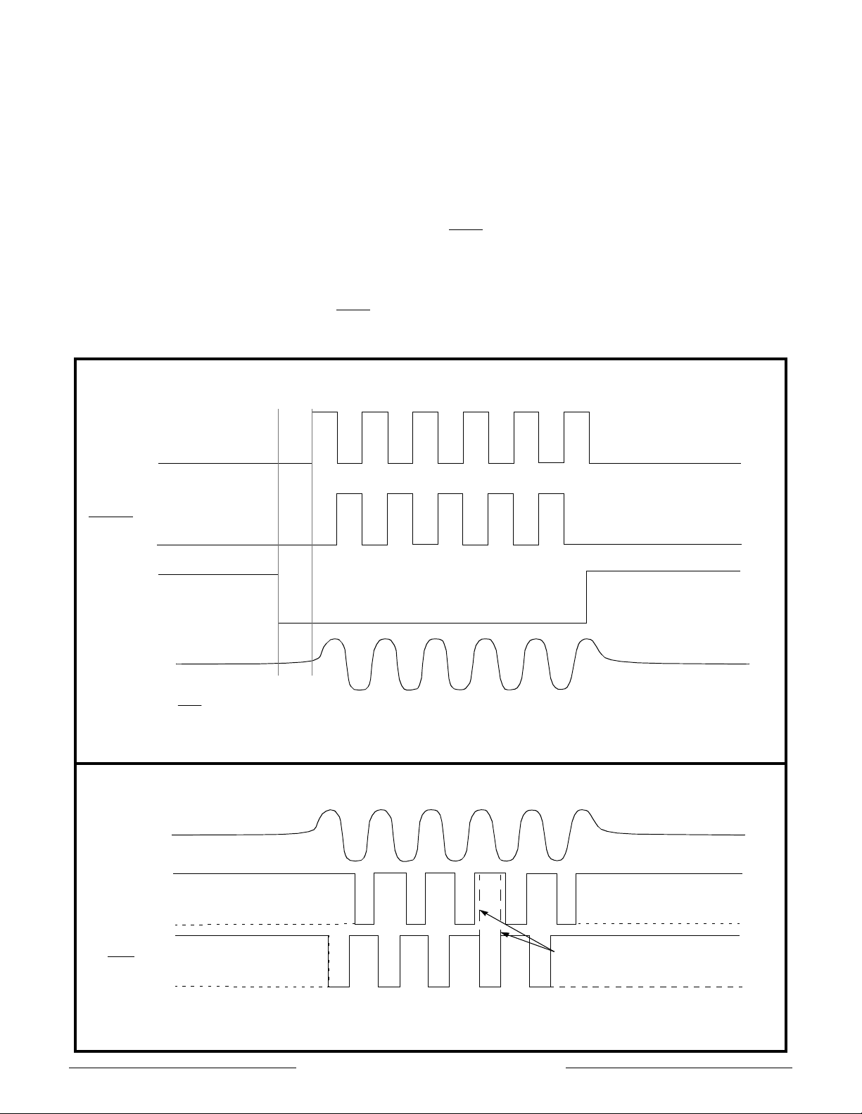
an overriding “INHIBIT” input returns the output
impedance to a high state. A logic “1” applied to the
“INHIBIT” takes priority over the condition of the data
inputs and disables the transmitter (See Transmitter
Logic Waveforms, Figure 1).
The transmitter utilizes an active filter to suppress
harmonics above 1 MHz to meet H009 Macair
specifications. The transmitter may be safely operated
for an indefinite period wi th the output shor t circuited
at 100% duty cycle.
Receiver
The Receiver section accepts bi-phase differential
data at the input and produces two TTL signals at the
output. The outputs are DATA and DATA
Figure 1 - Transmitter Logic Waveforms
Region 1 2 3
DATA IN
, and
represent positive and negative excursions of the
input beyond a pre-determined threshold (See
Receiver Logic Waveforms, Figure 2).
The internal threshold is nominally set to detect
data bus signals exceeding 1.05 Volts P-P and reject
signals less than 0.6 Volts P-P when used with a 1:1
turns ratio transformer (See Figure 5 for transformer
data and typical connection).
A low level at the Strobe input inhibits the DAT A and
DATA
outputs. If unused, a 2K pull-up to +5 Volts is
recommended.
DATA IN
INHIBIT
LINE TO LINE
OUTPUT
Notes: 1. Data and DATA inputs must be complementry waveforms or 50% duty cycle average, with no delays between them, and in the same state during
the off time (both high and low).
2. Region 1 ; no output signal, High Z state, (Receive Mode), Region 2; No Output signal, Low Z state, (Terminate Mode), Region 3, T ransmitter signal
on, low Z.
Figure 2 - Receiver Logic Waveforms
LINE TO LINE
INPUT
Rx DATA OUT
Rx DATA
Aeroflex Circuit Technology SCD4435N REV A 7/27/00 Plainview NY (516) 694-6700
OUT
Note: Waveforms shown are for normally low devices. For normally high receiver output
devices, the receiver outputs are swapped as shown by the dashed lines
level
2
Note overlap
Page 3

Absolu te Maximum Rat i ng s
Operating case temperature
Storage case temperature
Power supply Voltages
±15 V P.S. t o ± 1 8V MAX +5 V P.S. to +7V MAX
Logic input Voltage -0.3 V to +5.5 V
Receiver differential input
Receiver input voltage (common mode) ±10V
-55°C to +125°C
-65 °C to +150 °C
±40 V
Driver peak output current
Total package power dissipation over the full operating
case temperature range
Maximum junction to case temperature rise
(100 % duty cycle)
Junction-Case thermal resistance
150 mA
3.0 Watts
15°C
5°C/W
Electrical Characteristics, Transmitter Section
Input Characteristics, TX DATA in or TX DATA in
Parameter Condition Symbol Min Typ Max Unit
“0” Input Current VIN = 0.4 V I
“1” Input Current V
= 2.7 V I
IN
“0” Input Voltage V
“1” Input Voltage V
Inhibit Characteristics
"0" Input Current
"1" Input Current V
"0" Input Voltage
"1" Input Voltage V
Delay from TX inhibit(0→1) to inhibited output
Delay from TX inhibit, (1→0) to active output Note 1
V
=0.4V
IN
=2.7V I
IN
Note 1
ILD
IHD
IHD
IHD
I
ILI
IHI
V
ILI
IHI
t
DXOFF
t
DXON
2.0
2
-0.2 -0.4
1.0 40
0.7
-0.2
-0.4
1.0 40
0.7
350 700
200 500
mA
µA
V
V
mA
µA
V
V
nS
nS
Differential output noise, inhibit mode V
Differential output impedance (inhibited)
Note 2
Z
NOI
OI
10K Ω
0.8 10 mV p-p
Output Charact eris tics
Differential output level, pt A-A on Fig. 5
=170 Ω
R
L
Rise and fall times
(10% to 90% of p-p output), pt A-A on Fig. 5
Output offset at pt A-A on Fig. 5, 2.5 µS after
midpoint crossing of the last bit R
=170 Ω
L
Delay from 50% point of TX DATA or
TX DATA
input to zero crossing of differen-
tial signal. (note1)
Aeroflex Circuit Technology SCD4435N REV A 7/27/00 Plainview NY (516) 694-6700
3
V
V
t
DTX
t
OS
O
r
17 21 24 V p-p
200 300
nS
±265 mV peak
220 350 nS
Page 4

Electri cal C har act er is tic s, Receiver Sect io n
Parameter Condition Symbol Min Typ Max Unit
Differential Input Impedance (Note 1)
f= 1MHz
Differential Input Voltage Range V
Input Common Mode Voltage Range Note 1
Common Mode Rejection Ratio
Point A-A on
Figure 5
Strobe Characteristics (Logic “O” inhibits output)
"0" Input Current VS=0.4 V
"1" Input Current V
=2.7 V I
S
"0" Input Voltage
"1" Input Voltage
Strobe Delay (turn-on or turn-off)
Note 1.
Threshold Characteristics (Sinewave input)
Internal Threshold Voltage
(Referred to the bus) Pins 6 and 11 to GND
External Threshold
Pins 6 & 11 open, Pin 5 and Pin 12 with a 10K resistor to
GND, 1MHZ Sinewave applied to point A-A
100KHz-1MHz V
Z
IDR
V
ICR
CMRR
I
V
V
t
SD
TH
V
TH(
In
IL
IH
IL
IH
EXT
20K Ω
10
40 dB
-0.2
1.0 +40
2.0
0.60 0.80 1. 15 V
)
1.9 2.2 2.5 V
40
V p-p
V p-p
-0.4
mA
µA
0.7
V
V
150 nS
P-P
P-P
Output Characteristics, RX DATA and RX DATA
"1" State
"0" State I
Delay, (average) from differential input zero
crossings to RX DATA and RX DATA
output
50% points
=-0.4 mA
I
OH
= 4 mA V
OL
V
t
DRX
OH
OL
Power Data
Power Supply Currents (Power supplies set at +15V, -15V, +5V)
+V
Duty Cycle
Transmitter Standby
25% duty cycle
50% duty cycle
100% duty cycle
Recommended Power Supply Voltage Range
+V
-V -11.4 Volts to -15.75 Volts
Logic +4.5 Volt s to +5.5 Volts
ICC
TYP MAX TYP MAX TYP MAX
5mA 10mA 25m A
20mA 30mA 40mA 60mA
40mA 60mA 60mA
85mA 120mA 105mA 140mA
+11.4 Volts to +15.75 Volts
2.5 3.6 V
0.35
0.5
275 450 nS
-V
IEE
5V
IL
35mA
25mA 35mA
80mA
V
Aeroflex Circuit Technology SCD4435N REV A 7/27/00 Plainview NY (516) 694-6700
4
Page 5

Figure 3 – Transmitter (TX) Output Wave form Figure 4 – Transmitter (TX) Output offset
LAST BIT
2.5 µsec
90%
17V P-P MIN
24V P-P MAX
10%
tr*
* Rise and fall times measured at point A-A’ in Fig 5
tf*
0 Volts
0 volts
*Offset measured at point A-A’ in Fig 5
Figure 5 – Typical Transformer connection Figure 6 – Power Dissipation vs. Duty Cycle
4.0
3.5
3.0
2.5
2.0
1.5
POWER DISSIPATION
WA TTS
1.0
0.5
0
0 10 20 30 40 50 60 70 80 90 100
DUTY CYCLE, PERCENT
(TYPICAL)
TX DATA OUT
TX DATA
OUT
RX DATA
RX DATA IN
IN
35Ω
N1:N2
A
A’
35Ω
Transformer turns ratio:
N1:N2 = 1:1
Use Aeroflex 25T1553-1
170Ω
Magnified View
OUTPUT OFFSET*
OUTPUT OFFSET*
Notes:
1. Characteristics guaranteed by design, not prod uc t ion tested.
2. Measured at 1mHz at point A-A’, power on or off.
3. Specifications apply over the temperature range of -55°C to +125°C (case temperature)
unless otherwise not ed.
4. All typical values are measured at +25°C.
Aeroflex Circuit Technology SCD4435N REV A 7/27/00 Plainview NY (516) 694-6700
5
Page 6

CIRCUIT TECHNOLOGY
Package Configurations and Pinouts
PLUG-IN PACKAGE
1.27 M AX
1.10
24 13
1.27
MAX
Designator
Pin 1 & ESD
0.24
MIN
0.018 DI A.
±0.002
Notes
1. Dimensions shown are in inches.
2. Pins are equally spaced at 0.100±0.002 tolerance non-cumulative each row.
1.10
12
0.100
Pin Connections
1. TX D ATA OUT
2. TX D ATA
3. TX GND (+5V)
4. +15V (TX)
5. EXT. DATA THRES
6. INT. DATA TH RES
7. RX DATA OUT
8. STROBE
9. RX GND (+5V)
10. RXDATA
11. INT DATA
12. EXT DATA
13. +15V (RX)
14. N.C.
15. RX DATA IN
16. RX DATA
17. GND
18. CASE GND
0.175
19. -15V (RX)
MAX
20. +5V
21. TX INHIBIT
22. TX DATA IN
23. TX DATA
24. -15V (TX)
OUT
OUT
THRES
THRES
IN
IN
FLAT PACKAGE
1.27 M AX
Pin 1 & ESD
1.27 MAX
0.167 for Low Profile Flat Pack
0.200 for Std Flat Pack
Designator
±0.002
0.400
MAX
2 sides
0.009
±0.002
0.080 ±0.015
0.017
0.10 Typ
Confi g uratio ns and Ordering I n formation
Model No. DESC No.
Receiver Data level
Case
ARX4435N To Be Assigned Normally High Plug In H009 Macair
ARX4435N-FP To Be Assigned Normally High Flat Pack H009 Macair
The infor mation contained in this data sheet is believed to be accurate; however, Aeroflex Laborat ories Incorporated assumes no
responsibility for i ts use, and no license or rights are granted by implication or otherise in connection therewith.
Specifications subject to change without notice.
Aeroflex Circuit Technology
35 Sout h Servic e Roa d
Plainv iew New York 11803
www.aeroflex.com
Aeroflex Circuit Technology SCD4435N REV A 7/27/00 Plainview NY (516) 694-6700
6
Toll Free Inquiries: (800) 843- 1553
E-Mail: sales-act@aeroflex.com
Telephone: (516) 694-6700
FAX: (516) 694-6715
Specs.
 Loading...