

Page 1
Data Sheet (Preliminary)
Conexant Proprietary Information
Doc. No.100394B
October 19, 1999
AccessRunner
ADSL Modem Device Set for PCI Applications
Controller-less, Scalable, Discrete Multitone-based, G.dmt- and G.litecompliant, ADSL Modem Device Set for PCI Applications
Conexant’s AccessRunner ADSL modem device set is compliant
with the full-rate ANSI T1.413 Issue 2 and ITU G.dmt (G.992.1)
ADSL standards, and with the splitterless ITU G.lite (G.992.2)
specification. This rate-adaptive solution is designed for controllerless PCI desktop applications and supports downstream data rates
of up to 8 Mbps and upstream data rates of up to 1 Mbps.
The device set takes advantage of the processing power available
with most new computers by eliminating the need for a separate
microcontroller, resulting in a cost-effective solution suitable for
both G.dmt and G.lite applications. Host-based software provides
support for current industry standards for PPP over AAL5 over
ATM over ADSL and RFC 1483 for Windows 98 and Windows
2000.
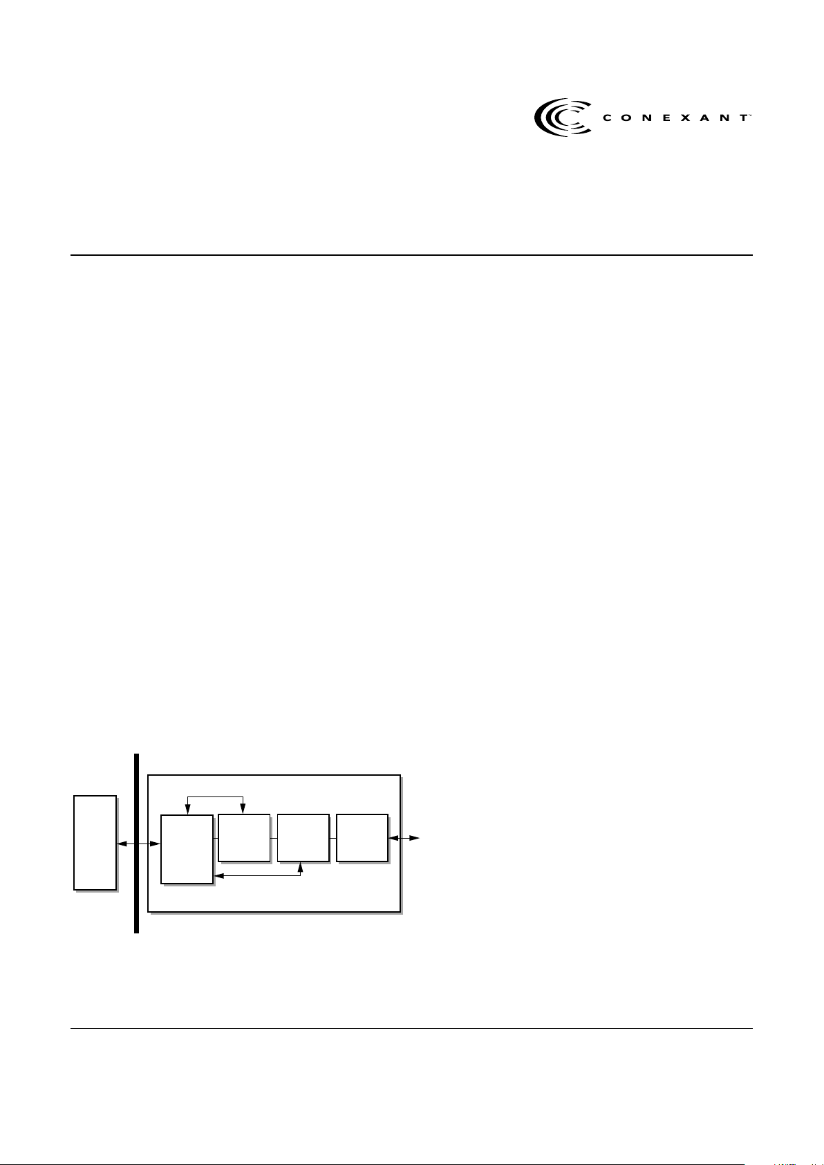
The device set, as shown in Figure 1, consists of four chips:
•
PCI bus interface (AccessRunner P46 in a 176-pin TQFP)
•
DMT-based data pump (AccessRunner 11627 in a 176-pin
TQFP)
•
Analog front end (AccessRunner 20431 in a 32-pin TQFP)
•
Line driver (AccessRunner 20441 in a 16-pin SSOP or
32-pin TQFP)
PCI Bus
HostBased
ADSL
Controller
Software
P46
PCI Bus
Interface
176-pin TQFP
11627
ADSL DMT
Data Pump
176-pin TQFP
20431
Analog Front
End
32-pin TQFP
20441
Line Driver
16-pin TSSOP
Telephone
Line
Figure 1. AccessRunner ADSL Modem for PCI Applications
Features
•
Complete controller-less PCI ADSL
solution
•
Compliant with ADSL standards
−
Full-rate ANSI T1.413 Issue 2 and ITU
G.dmt (G.992.1) standards
−
Splitterless ITU G.lite (G.992.2)
specification
•
DMT modulation and demodulation
•
Full-rate adaptive modem
−
Maximum downstream rate of 8 Mbps
−
Maximum upstream rate of 1 Mbps
•
Supports splitterless ADSL
implementation
•
WAN mode support: PPP over AAL5/ATM
over ADSL via Windows 98/2000
•
LAN mode support: RFC 1483 via
Windows 98/2000
•
Compliant with PCI Local Bus
Specification, Revision 2.2
•
Compliant with PCI Bus Power
Management Interface Specification,
Version 1.0
•
Tone detection for low power mode
D20431 AFE Features
•
Receive signal path includes:
−
Integrated hybrid receiver circuit with
programmable gain
−
High pass filtering and 27dB of
Automatic Gain Control (AGC) to
improve signal-to-echo ratio
−
14-bit ADC
•
Transmit signal path includes:
−
30dB of AGC for transmit power control
−
Low pass filtering to suppress noise in
the receive band
−
14-bit DAC
•
Independent digital serial data and control
interfaces
•
Low power tone detection mode.
Page 2
AccessRunner
Controller-less ADSL Modem Device Set for PCI Applications
2
Conexant
Doc. No. 100394B
Proprietary Information October 19, 1999
ADSL (Asymmetric Digital Subscriber Line) is a transmission
technology used to carry user data over a single twisted pair line
from the Central Office to the customer premises. The downstream
(Central Office to Customer Premises) direction typically supports
a much higher data rate than the upstream or return (Customer
Premises to Central Office) channel. This asymmetric nature lends
itself to applications like remote LAN access, Internet access, and
video delivery. The downstream data rates can go up to 8 Mbps.
The upstream data rates can go up to 1 Mbps. Actual data rates
depend on the transceiver implementation, loop length,
impairments, and transmitted power.
The Conexant ADSL Modem Device Set for PCI Applications is
based upon a scalable architecture. This architecture will enable
the device set to support an emerging set of ADSL specifications
called G.lite. G.lite is expected to make it possible for telcos to
deploy consumer-oriented, “always on” 1.5 Mbps Internet access
services without the need for splitter equipment or wiring changes
at the customer premises.
D20441 Line Driver Features
•
Differential input and output line driver
•
Thermal shutdown capability
•
Line impedance matching during powerdown
•
Fixed differential gain
11627 ADSL DMT Data Pump
Features
•
Low power (0.5W) consumption
•
DSP-based programmable ADSL data
pump
•
No external Interleave RAM, 16 Kbytes
built-in
•
Single 3.3V ± 5% power supply
•
Echo cancellation
•
Digital interface and rate buffering
•
ADSL framing
•
Forward Error Correction (FEC) encoding
and decoding and interleaving
•
Constellation encoding/decoding
•
IFFT modulation and FFT demodulation
•
Transmit and receive signal digital filtering
•
Time domain equalization
•
Frequency domain equalization
•
Clock recovery
•
CRC and scrambling
•
Digital interface framing
•
ATM mode
•
Bit-synchronous mode
Ordering Information
Product Package Device Number
AccessRunner P46
PCI Bus Interface 176-pin TQFP P46
AccessRunner 11627
ADSL Discrete Multit one (DM T ) Dat a Pump 176-pin TQFP 11627
AccessRunner 20431
Analog Front End 32-pin TQFP 20431
16-pin SSOP 20441-12
AccessRunner 20441
Line Driver
32-pin TQFP 20441-11
Revision History
Revision Date Comments
A 07/09/99 Initial release
B 10/19/99 Defined dash numbers and updated figures f or 20441 l ine driver, changed document number f rom DS L-
015, A
Information provided by Conexant Systems, Inc. is believed to be accurate and reliable. However, no responsibility is assumed by Conexant for its use, nor any
infringement of patents or other rights of third parties which may result from its use. No license is granted by implication or otherwise under any patent rights of
Conexant other than for circuitry embodied in Conexant products. Conexant reserves the right to change circuitry at any time without notice. This document is
subject to change without notice.
Conexant products are not designed or intended for use in life support appliances, devices, or systems where malfunction of a Conexant product can reasonably be
expected to result in personal injury or death. Conexant customers using or selling Conexant products for use in such applications do so at their own risk and agree
to fully indemnify Conexant for any damages resulting from such improper use or sale.
Conexant, “What's Next in Communications Technologies”, AccessRunner, LANfinity, and the Conexant logo, are trademarks of
Conexant Systems, Inc.
Product names or services listed in this publication are for identification purposes only, and may be trademarks or registered trademarks of their respective
companies. All other marks mentioned herein are the property of their respective owners.
©1999, Conexant Systems, Inc.
All Rights Reserved
Page 3
Controller-less ADSL Modem Device Set for PCI Applications AccessRunner
Doc. No. 100394B
Conexant
3
October 19, 1999 Proprietary Information
Detailed Description
P46 PCI Bus Interface
The P46 PCI bus interface is the bridge device
between the 11627 ADSL DMT data pump and the
host computer. It provides the control, interface, and
data manipulation for the 11627 data pump, the
20431 AFE, the 20441 line driver, and hybrid
circuitry. It is compliant with the PCI Local Bus
Specification, Revision 2.2 and PCI Bus Power
Management Interface Specification, Version 1.0.
20431 Analog Front End
The 20431 AFE is designed for use in full-rate and
G.lite (G.992.2) ADSL modems. The ADSL AFE
interfaces with the transmit line driver (20441) and
the hybrid receive circuitry on the analog side, and
with the ADSL DMT data pump (11627) on the digital
side. The receive section filters out the unwanted
echo and boosts the wanted signal before
performing an A/D conversion. The transmit section
converts digital data to analog signals and performs
a smoothing operation before presenting the signals
to the line driver.
The 20431 is designed to operate from a 3.3V supply
(nominal), assuming that it is regulated within ± 5%. The
maximum allowable supply voltage is 3.6V.
11627 ADSL DMT Data Pump
The 11627 DMT data pump is a T1.413 Issue 2 and
G.992.1 compliant custom digital signal processing
(DSP) chip built specifically for DMT ADSL
transmission for use in ADSL modems. Brief
descriptions of each functional block within the data
pump are provided in the following sections; refer to
Figure 2.
ATM Transmission Convergence (TC)
In the transmit direction, this block is in charge of
embedding ATM cells into the serial data streams
being fed into the digital interface.
In the receive direction, this block extracts the ATM
cell boundaries from the serial data streams coming
from the digital interface.
To reduce traffic on the PCI bus, the TC block
performs idle cell insertion in the transmit direction
and idle cell deletion and header error correction in
the receive direction.
DSL015002
ATM TC
DI
Transmit
Block
DI
Receive
Block
Digital
Interface (DI)
Bit Parser
and QAM
Encoder
QAM
Decoder
and Bit
Parser
AM EncoderDecoder
FEQ
IFFT
FFT
FFT
Transmit
Filter
Time
Domain
Equalizer
ADC
Intf
AFE Interface
DAC
Intf
PCI
Controller
(P46)
Microcontroller
Interface
AFE
(20431)
DMT Data Pump (11627)
EC
Figure 2. AccessRunner 11627 DMT Data Pump Functional Block Diagram
Page 4
AccessRunner
Controller-less ADSL Modem Device Set for PCI Applications
4
Conexant
Doc. No. 100394B
Proprietary Information October 19, 1999
Digital Interface (DI)
The DI Transmit Block performs the following
functions: transmit data multiplexing and buffering,
fast and interleave data stream framing, transmit
data synchronization control, eoc/aoc insertion, CRC
encoding, scrambling, FEC encoding, and data
interleaving.
The DI Receive Block performs the following
functions: data de-interleaving, FEC decoding,
descrambling, CRC check, receive data
synchronization and receive clock generation,
demultiplexing and buffering of receive data and
receive eoc/aoc.
QAM Encoder/Decoder
The QAM Encoder/Decoder performs the following
functions: constellation encoding, clock recovery,
receive gain compensation, frequency domain
equalization (FEQ), slicing, and constellation
decoding. The block also performs other functions
like frequency domain signal processing, signal
power, error power averaging and computations
related to frequency domain training.
FFT
The FFT performs IFFT for modulation of the
transmit symbol, and FFT for demodulation of the
receive symbol.
Analog Front End (AFE) Interface
The AFE Interface performs the following functions:
transmit signal filtering, time domain equalization,
and time domain signal power averaging, and echo
cancellation (EC).
Microcontroller Interface
The microcontroller interface enables the host
computer via the PCI controller to set parameters to
control DSP sequencing and to read/write
coefficients or data.
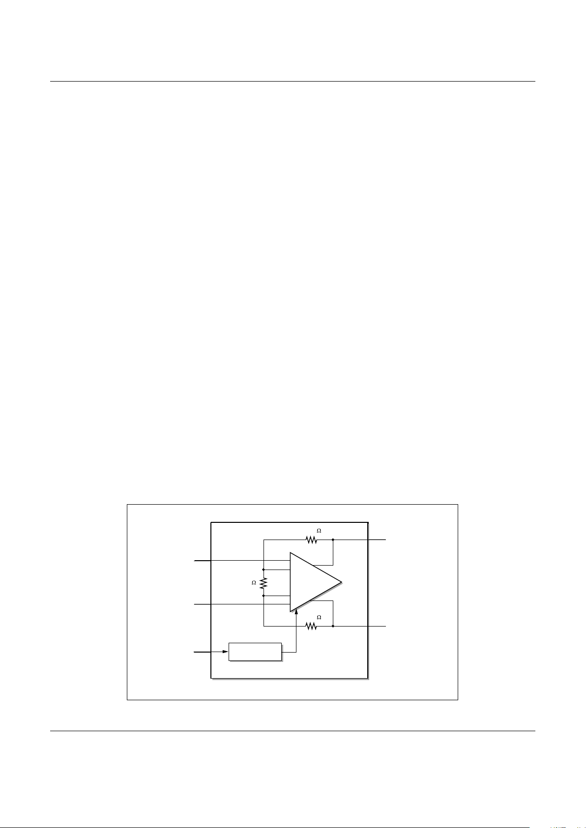
20441 Line Driver
The 20441 line driver is designed for use in full-rate
and G.lite (G.992.2) ADSL modems. It is optimized
for ideal ADSL performance providing low noise,
high bandwidth, and superior linearity. The 20441
line driver transmits a DMT modulated signal in the
25 – 132 kHz band. It operates from a single 5V
±TBD% supply, refer to
Figure 3.
The driver is optimized for ADSL performance: it has
a very low noise figure, high bandwidth and good
linearity.
()
Current Control
Block
Line Driver
(20441)
+
+
+
248.4
248.4
400
OUTP_DRV
OUTM_DRV
INP_DRV
INM_DRV
RBIAS
DSL015_003
Figure 3. AccessRunner 20441 Line Driver
Page 5
Controller-less ADSL Modem Device Set for PCI Applications AccessRunner
Doc. No. 100394B
Conexant
5
October 19, 1999 Proprietary Information
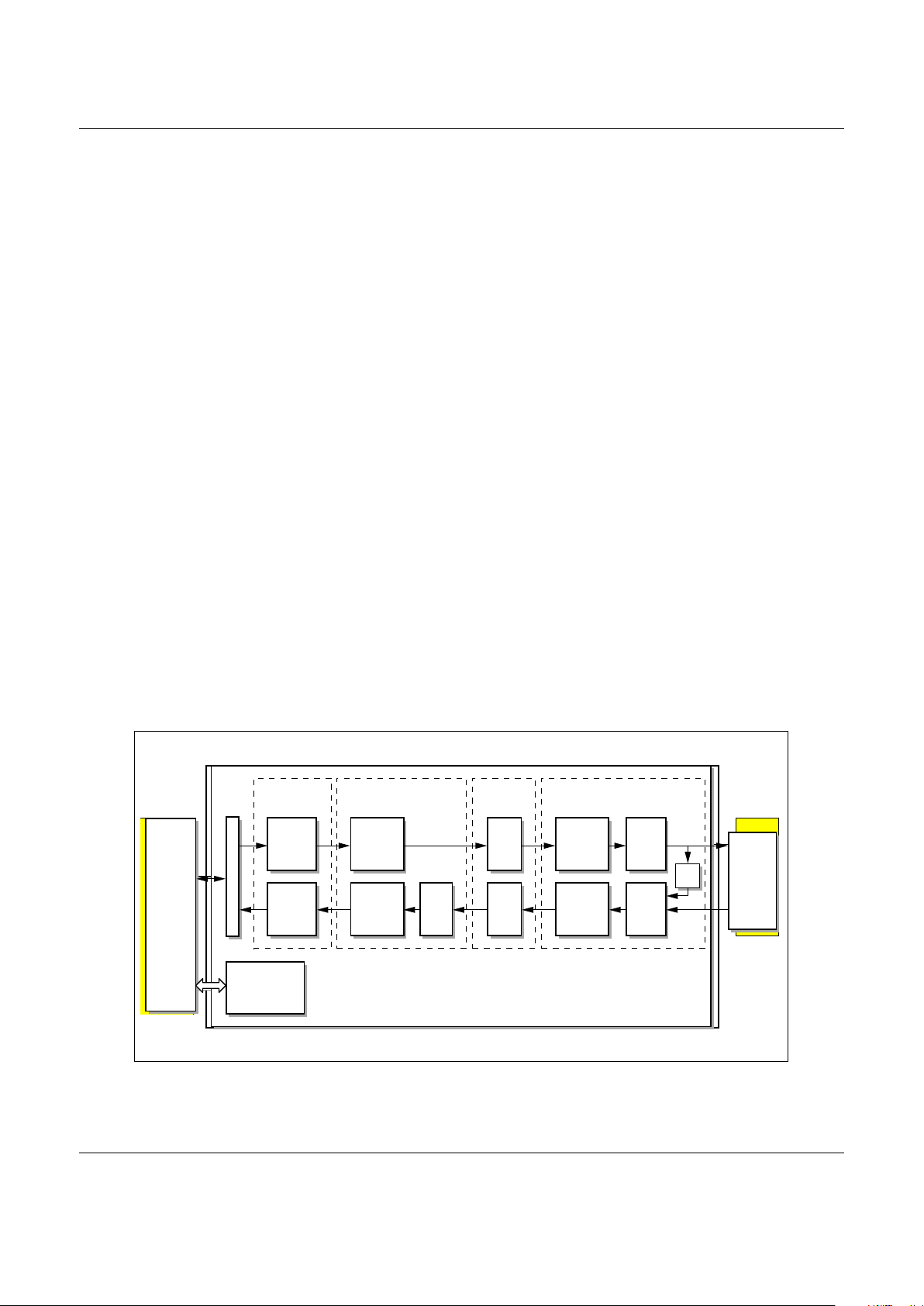
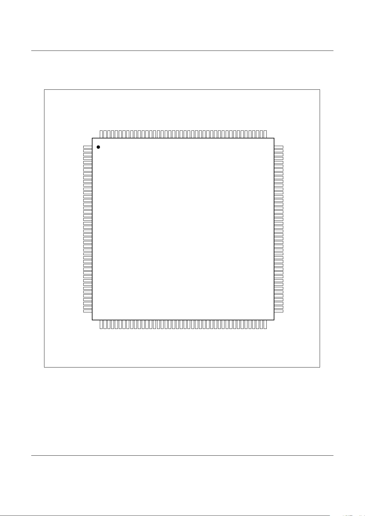
P46 PCI Bus Interface Device Hardware Pins and Signals
The pin assignments for the P46 are shown in Figure 4 and listed in Table 1. The signals are defined in Table 2.
45464748495051525354555657585960616263646566676869707172737475767778798081828384858687
88
132
131
130
129
128
127
126
125
124
123
122
121
120
119
118
117
116
115
114
113
112
111
110
109
108
107
106
105
104
103
102
101
100
99
98
97
96
95
94
93
92
91
90
89
1
2
3
4
5
6
7
8
9
10
11
12
13
14
15
16
17
18
19
20
21
22
23
24
25
26
27
28
29
30
31
32
33
34
35
36
37
38
39
40
41
42
43
44
176
175
174
173
172
171
170
169
168
167
166
165
164
163
162
161
160
159
158
157
156
155
154
153
152
151
150
149
148
147
146
145
144
143
142
141
140
139
138
137
136
135
134
133
VDD
DP_WR#
DP_A[0]
DP_A[1]
DP_A[2]
DP_A[3]
DP_A[4]
DP_A[5]
DP_A[6]
DP_A[7]
GND
DP_A[8]
DP_A[9]
VDD
DP_IRQ#[0]
DP_IRQ#[1]
AFE_WAKEUP
AFE_CTRLOUT
AFE_CTRLIN
AFE_STB
AFE_SCLK
GND
DP_RDATAS0
DP_RXSOC0
VDD
DP_RCLKAS0
DP_TDATLS0
DP_TXSOC0
DP_TCLKLS0
GND
NC
VDD
PCI_VAUXDET
PCI_VPCIDET
NC
PCI_VAUXEN#
PCI_VPCIEN#
NC
SCANMODE
SCANEN
GNDNCNC
NC
VDD
PCI_AD[7]
PCI_AD[6]
GND
PCI_AD[5]
PCI_AD[4]
VDD
PCI_AD[3]
PCI_AD[2]
GND
PCI_AD[1]
PCI_AD[0]
VDD
PCI_PME
EEPROM_DIN
EEPROM_DOUT
EEPROM_CLK
EEPROM_CS
VDD
VGG2
DP_D[0]
DP_D[1]
GND
DP_D[2]
DP_D[3]
GND
DP_D[4]
DP_D[5]
VDD
DP_D[6]
DP_D[7]
DP_D[8]
DP_D[9]
DP_D[10]
DP_D[11]
GND
DP_D[12]
DP_D[13]
VDD
DP_D[14]
DP_D[15]
DP_CS#
DP_RD#
GND
VDD
PCI_AD[24]
PCI_CBE#[3]
PCI_IDSEL
GND
PCI_AD[23]
PCI_AD[22]
VDD
PCI_AD[21]
PCI_AD[20]
GND
PCI_AD[19]
PCI_AD[18]
VDD
PCI_AD[17]
PCI_AD[16]
GND
PCI_AD[15]
PCI_CBE#[2]
VDD
PCI_FRAME#
PCI_IRDY#
GND
PCI_TRDY#
PCI_DEVSEL#
PCI_STOP#
PCI_PERR#
VDD
PCI_SERR#
PCI_PAR
PCI_CBE#[1]
GND
PCI_AD[14]
PCI_AD[13]
VDD
PCI_AD[12]
PCI_AD[11]
GND
PCI_AD[10]
PCI_AD[9]
VDD
PCI_AD[8]
PCI_CBE#[0]
GND
PCI_INTA#
PCI_RST#
VDD
PCI_CLK
GND
PCI_GNT#
PCI_REQ#
PCI_AD[31]
VDD
PCI_AD[30]
PCI_AD[29]
GND
PCI_AD[28]
PCI_AD[27]
VDD
PCI_AD[26]
PCI_AD[25]
GND
VGG1
VDD
GPIN0
GPIN1
GPIO[0]
GPIO[1]
GPIO[2]
GPIO[3]
GND
VDD
GPIO[4]
GPIO[5]
GPIO[6]
GPIO[7]
GND
VDD
GPIO[8]
GND
TDI_GPIO[9]
TMS_GPIO[10]
VDD
TRSTN_GPIO[11]
REFCLK
PCI_VPCIPREFER
TCK
TDO
DSL015004
Figure 4. P46 Pinout Diagram
Page 6

AccessRunner
Controller-less ADSL Modem Device Set for PCI Applications
6
Conexant
Doc. No. 100394B
Proprietary Information October 19, 1999
Table 1. P46 Pin Designations by Number
Pin No. Signal Pin No. Signal Pin No. Signal Pin No. Signal
1 VDD 45 VDD 89 VDD 133 VDD
2 GPIN0 46 PCI_AD[24] 90 PCI_AD[7] 134 DP_WR#
3 GPIN1 47 PCI_CBE#[3] 91 PCI_AD[6] 135 DP_A[0]
4 GPIO[0] 48 PCI_IDSEL 92 GND 136 DP_A[1]
5 GPIO[1] 49 GND 93 PCI_AD[5] 137 DP_A[2]
6 GPIO[2] 50 PCI_AD[23] 94 PCI_AD[4] 138 DP_A[3]
7 GND 51 PCI_AD[22] 95 VDD 139 DP_A[4]
8 GPIO[3] 52 VDD 96 PCI_AD[3] 140 DP_A[5]
9 GPIO[4] 53 PCI_AD[21] 97 PCI_AD[2] 141 DP_A[6]
10 VDD 54 PCI_AD[20] 98 GND 142 DP_A[7]
11 GPIO[5] 55 GND 99 PCI_AD[1] 143 GND
12 GPIO[6] 56 PCI_AD[19] 100 PCI_AD[0] 144 DP_A[8]
13 GPIO[7] 57 PCI_AD[18] 101 VDD 145 DP_A[9]
14 GPIO[8] 58 VDD 102 PCI_PME 146 VDD
15 GND 59 PCI_AD[17] 103 VGG2 147 DP_IRQ#[0]
16 TDI_GPIO[9] 60 PCI_AD[16] 104 EEPROM_DIN 148 DP_IRQ#[1]
17 TMS_GPIO[10] 61 GND 105 EEPROM_DOUT 149 AFE_WAKEUP
18 VDD 62 PCI_AD[15] 106 EEPROM_CLK 150 AFE_CTRLOUT
19 REFCLK 63 PCI_CBE#[2] 107 EEPROM_CS 151 AFE_CTRLIN
20 TRSTN_GPIO[11] 64 VDD 108 VDD 152 AFE_STB
21 PCI_VPCIPREFER 65 PCI_FRAME# 109 DP_D[0] 153 AFE_SCLK
22 VDD 66 PCI_IRDY# 110 DP_D[1] 154 GND
23 TCK 67 GND 111 GND 155 DP_RDATAS0
24 TDO 68 PCI_TRDY# 112 DP_D[2] 156 DP_RXSOC0
25 GND 69 PCI_DEVSEL# 113 DP_D[3] 157 VDD
26 PCI_INTA# 70 PCI_STOP# 114 GND 158 DP_RCLKAS0
27 PCI_RST# 71 PCI_PERR# 115 DP_D[4] 159 DP_TDATLS0
28 VDD 72 VDD 116 DP_D[5] 160 DP_TXSOC0
29 PCI_CLK 73 PCI_SERR# 117 VDD 161 DP_TCLKLS0
30 GND 74 PCI_PAR 118 DP_D[6] 162 GND
31 PCI_GNT# 75 PCI_CBE#[1] 119 DP_D[7] 163 PCI_VAUXDET
32 PCI_REQ# 76 GND 120 DP_D[8] 164 PCI_VPCIDET
33 PCI_AD[31] 77 PCI_AD[14] 121 DP_D[9] 165 VDD
34 VDD 78 PCI_AD[13] 122 DP_D[10] 166 NC
35 PCI_AD[30] 79 VDD 123 GND 167 NC
36 PCI_AD[29] 80 PCI_AD[12] 124 DP_D[11] 168 NC
37 GND 81 PCI_AD[11] 125 DP_D[12] 169 NC
38 PCI_AD[28] 82 GND 126 VDD 170 NC
39 PCI_AD[27] 83 PCI_AD[10] 127 DP_D[13] 171 NC
40 VGG1 84 PCI_AD[9] 128 DP_D[14] 172 PCI_VAUXEN#
41 VDD 85 VDD 129 DP_D[15] 173 PCI_VPCIEN#
42 PCI_AD[26] 86 PCI_AD[8] 130 DP_CS# 174 SCANMODE
43 PCI_AD[25] 87 PCI_CBE#[0] 131 DP_RD# 175 SCANEN
44 GND 88 GND 132 GND 176 GND
Page 7

Controller-less ADSL Modem Device Set for PCI Applications AccessRunner
Doc. No. 100394B
Conexant
7
October 19, 1999 Proprietary Information
Table 2. P46 Pin Signals by Group
Pin Name I/O
1
Description
PCI INTERFACE
PCI_AD[31:0] I/O Address/Data
PCI_CBE#[3:0] I/O Command/Byte Enables
PCI_FRAME# I/O Frame
PCI_IRDY# I/O Initiat or Ready
PCI_TRDY# I/O Target Ready
PCI_PAR I/O Parity (Even)
PCI_STOP# I/O Target Stop
PCI_DEVSEL# I/O Target Response Device Select
PCI_IDSEL I Unique Select for Configuration
PCI_PERR# I/O Parity Error
PCI_SERR# O System Error
PCI_REQ# O Master Request
PCI_GNT# I Grant
PCI_CLK I PCI clock
PCI_RST# I (S) Reset
PCI_INTA# O Interrupt A
PCI_PME O PCI Power Management Event Signal
ADSL DMT DATA PUMP (11627) SERIAL CHANNEL INTERFACE
DP_RDATAS0 I Receive AS0/ATM0 Serial Data
DP_RXSOC0 I Receive ATM0 S tart of Cell
DP_RCLKAS0 I Receive AS0/ATM0 Data Clock
DP_TDATLS0 O Transmit LS0/ATM0 Seri al Data
DP_TXSOC0 O Transmit ATM0 Start of Cel l
DP_TCLKLS0 I Transmit LS 0/ATM0 Data Clock
ADSL DMT DATA PUMP (11627) MICRO INTERFACE
DP_WR# O Data Pump Device Write Enable
DP_RD# O Data Pump Device Read Enable
DP_D[15:0] I/O (PU) Data Pump Data Lines
DP_A[9:0] O Data Pump A ddress Lines
DP_CS# O Data Pump Chip Sel ect
DP_IRQ#[1:0] I (PU,S) Data Pump Interrupt Request Lines
ANALOG FRONT END INTERFACE
AFE_SCLK I Serial AFE Clock
AFE_STB O AFE Strobe
AFE_CTRLIN O Serial Data Sent to AFE
AFE_CTRLOUT I Serial Data Received from AFE
1
PD Resistive pull-down
PU Resis tive pull-up
S Schmitt
Page 8

AccessRunner
Controller-less ADSL Modem Device Set for PCI Applications
8
Conexant
Doc. No. 100394B
Proprietary Information October 19, 1999
Pin Name I/O
1
Description
AFE_WAKEUP I (S) DSL Power Management Wakeup Signal from AFE
SERIAL EEPROM
EEPROM_CS O EEPROM Chip Select
EEPROM_CLK O EEPROM Clock
EEPROM_DIN I EEPROM Data Input
EEPROM_DOUT O EEPROM Data Output
PCI POWER MANAGEMENT
PCI_VAUXDET I (PD,S) Vaux Detect
PCI_VPCIDET I (PD,S) Vpci Detect
PCI_VAUXEN# O Vaux Enable
PCI_VPCIEN# O Vpci Enable
PCI_VPCIPREFER I This pin is used to determine whether Vpci or Vaux is the preferred power suppl y.
1=Vpci preferred, 0=Vaux preferred
MISCELLANEOUS
GPIO[1:0] I/O (PU,S) General Purpose Schmitt I nput /Output
GPIO[2:5], GPIO[8] I/O (PU) General Purpose Input/Output
GPIO[6] I/O General Purpose Input/Output (also used for act i ve low reset)
GPIO[7] I/O General Purpose Input/Output (also used for acti ve high reset)
TDI_GPIO[9] I / O (P U) JTAG test data i nput OR general purpose input/output. Functi on of this pin is
dependant upon value of JTAGEN bit. When operating in JTAG mode this signal
contains serial data that i s shifted in on the rising edge of TCK.
TMS_GPIO[10] I/O (PU) JTAG test mode select OR general purpose input/output.
Function of this pin is dependant upon value of JTAGEN bit. When operating in JTAG
mode this siganl controls the operation of the TAP cont rol l er.
TRSTN_GPIO[11] I/O (PU) JTAG reset OR general purpose i nput/output.
Function of this pin is dependant upon value of JTAGEN bit. When operating in JTAG
mode, a high to low transition on t hi s signal forces the TAP controller into a logic reset
state.
TCK I JTAG clock.
TDO O JTAG data output. This pin generates serial data that is shifted out on t he f alling edge
of TCK..
GPIN0 I (S) General purpose schmitt input (m odem ri ng det ect)
GPIN1 I (PU,S) General purpos e schmitt input (modem of fhook)
SCANEN I (PD) Scan chain enable. Used to s hi f t data in and out of the scan c hai n.
SCANMODE I (PD) Scan mode enable pin. When tied high it will put the device into scan t est mode.
REFCLK I 35.328 MHz reference clock used to create the internal 53 MHz system clock
POWER AND GROUND
VDD 3.3V Power
GND Ground
VGG1 I/O Clamp Power Supply for PCI Signalling Environment (connect to VIO pin of PCI
Bus)
VGG2 I/O Clamp Power Supply for B ackend (connect to 3.3 vol t supply)
Page 9

Controller-less ADSL Modem Device Set for PCI Applications AccessRunner
Doc. No. 100394B
Conexant
9
October 19, 1999 Proprietary Information
11627 ADSL DMT Data Pump Hardware Pins and Signals
The pin assignments for the 11627 are shown in Figure 5 and listed in Table 3. The signals are defined in
Table 4.
1
2
3
4
5
6
7
8
9
10
11
12
13
14
15
16
17
18
19
20
21
22
23
24
25
26
27
28
29
30
31
32
33
34
35
36
37
38
39
40
41
42
43
44
45
46
47
48
49
50
51
52
53
54
55
56
57
58
59
60
61
62
63
64
65
66
67
68
69
70
71
72
73
74
75
76
77
78
79
80
81
82
83
84
85
86
87
88
132
131
130
129
128
127
126
125
124
123
122
121
120
119
118
117
116
115
114
113
112
111
110
109
108
107
106
105
104
103
102
101
100
99
98
97
96
95
94
93
92
91
90
89
176
175
174
173
172
171
170
169
168
167
166
165
164
163
162
161
160
159
158
157
156
155
154
153
152
151
150
149
148
147
146
145
144
143
142
141
140
139
138
137
136
135
134
133
GND
DAC_CLK
FILTER_CLK
T_FAST_BYTE#
T_INTER_BYTE#
R_CLK_AS1
NC
NTR
GND
VDD
R_CLK_AS0
NC
T_CLK_LS1
T_DAT_LS1
T_CLK_LS0
T_DAT_LS0
BIT_CLOCK
GND
GND
GND
TXSOC0
TLXCK_EN
TXSOC1
AFE_STR#
VDDcore
VDDcore
VDD
GND
NTRCTL
DMCK_ALT
R_INTER_SUPER#
R_INTER_DATA
R_FAST_SUPER#
R_FAST_FRAME#
GND
VDD
R_NCO_LS0
R_NCO_LS1
R_NCO_AS0
R_NCO_AS1
R_DAT_AS0
R_DAT_AS1
NC
NC
VDD
GND
RX[1]
RX[0]
ADC_CLK
D[0]
D[1]
D[2]
D[3]
D[4]
VDD
GND
D[5]
D[6]
D[7]
D[8]
D[9]
D[10]
D[11]
D[12]
D[13]
D[14]
VDD
VDDcore
VDDcore
GND
GND
GND
D[15]
VGG
A[0]
A[1]
A[2]
A[3]
A[4]
A[5]
A[6]
A[7]
A[8]
VDDcore
GND
A[9]
W
R#
VDD
RXSOC0
RXSOC1
R_CLK_LS0
R_DAT_LS0
R_CLK_LS1
R_DAT_LS1
NC
GND
GND
VDD
NC
NC
NC
NC
VDDcore
VDDcore
VDDcore
GND
GND
GND
NC
VCXO_CTRL
MON_DONE
MCLK
VDD
VDDcore
VDDcore
GND
GND
GND
GND
VDD
M
ON_OUT
MON_CLK
PW
R_DN
NC
LTR
IRQ[1]#
IRQ[0]#
CLIP#
RST#
RD#
CS#
GND
VDD
GND
TX[15]
TX[14]
TX[13]
TX[12]
TX[11]
TX[10]
VDD
GND
TX[9]
TX[8]
TX[7]
TX[6]
TX[5]
TX[4]
TX[3]
TX[2]
TX[1]
TX[0]
VDD
VDDcore
VDDcore
GND
GND
GND
RX[15]
RX[14]
RX[13]
RX[12]
RX[11]
RX[10]
RX[9]
RX[8]
RX[7]
RX[6]
VDDcore
GND
RX[5]
RX[4]
RX[3]
RX[2]
VDDcore
GND
DSL015_005
Figure 5. 11627 Pinout Diagram
Page 10

AccessRunner
Controller-less ADSL Modem Device Set for PCI Applications
10
Conexant
Doc. No. 100394B
Proprietary Information October 19, 1999
Table 3. 11627 Pin Designations by Number
Pin No. Signal Pin No. Signal Pin No. Signal Pin No. Signal Pin No. Signal
1 GND 37 R_NCO_LS0 73 GND 109 VDDcore 145 RX[10]
2 DAC_CLK 38 R_NCO_LS1 74 GND 110 VDD 146 RX[11]
3 FILTER_CLK 39 R_NCO_AS0 75 GND 111 D[14] 147 RX[12]
4 T_FAST_BYTE# 40 R_NCO_AS1 76 VDD 112 D[13] 148 RX[13]
5 T_INTER_BYTE# 41 R_DAT_AS0 77 MON_OUT 113 D[12] 149 RX[14]
6 R_CLK_AS1 42 R_DAT_AS1 78 MON_CLK 114 D[11] 150 RX[15]
7 NC 43 NC 79 PWR_DN 115 D[10] 151 GND
8 NTR 44 NC 80 NC 116 D[9] 152 GND
9 GND 45 RXSOC0 81 LTR 117 D[8] 153 GND
10 VDD 46 RXSOC1 82 IRQ[1]# 118 D[7] 154 VDDcore
11 R_CLK_AS0 47 R_CLK_LS0 83 IRQ[0]# 119 D[6] 155 VDDcore
12 NC 48 R_DAT_LS0 84 CLIP# 120 D[5] 156 VDD
13 T_CLK_LS1 49 R_CLK_LS1 85 RST# 121 GND 157 TX[0]
14 T_DAT_LS1 50 R_DAT_LS1 86 RD# 122 VDD 158 TX[1]
15 T_CLK_LS0 51 NC 87 CS# 123 D[4] 159 TX[2]
16 T_DAT_LS0 52 GND 88 GND 124 D[3] 160 TX[3]
17 BIT_CLOCK 53 GND 89 VDD 125 D[2] 161 TX[4]
18 GND 54 VDD 90 WR# 126 D[1] 162 TX[5]
19 GND 55 NC 91 A[9] 127 D[0] 163 TX[6]
20 GND 56 NC 92 GND 128 ADC_CLK 164 TX[7]
21 TXSOC0 57 NC 93 VDDcore 129 RX[0] 165 TX[8]
22 TLXCK_EN 58 NC 94 A[8] 130 RX[1] 166 TX[9]
23 TXSOC1 59 VDDcore 95 A[7] 131 GND 167 GND
24 AFE_STR# 60 VDDcore 96 A[6] 132 VDD 168 VDD
25 VDDcore 61 VDDcore 97 A[5] 133 GND 169 TX[10]
26 VDDcore 62 GND 98 A[4] 134 VDDcore 170 TX[11]
27 VDD 63 GND 99 A[3] 135 RX[2] 171 TX[12]
28 GND 64 GND 100 A[2] 136 RX[3] 172 TX[13]
29 NTRCTL 65 NC 101 A[1] 137 RX[4] 173 TX[14]
30 DMCK_ALT 66 VCXO_CTRL 102 A[0] 138 RX[5] 174 TX[15]
31 R_INTER_SUPER# 67 MON_DONE 103 VGG 139 GND 175 GND
32 R_INTER_DATA 68 MCLK 104 D[15] 140 VDDcore 176 VDD
33 R_FAST_SUPER# 69 VDD 105 GND 141 RX[6]
34 R_FAST_FRAME# 70 VDDcore 106 GND 142 RX[7]
35 GND 71 VDDcore 107 GND 143 RX[8]
36 VDD 72 GND 108 VDDcore 144 RX[9]
Page 11

Controller-less ADSL Modem Device Set for PCI Applications AccessRunner
Doc. No. 100394B
Conexant
11
October 19, 1999 Proprietary Information
Table 4. 11627 Pin Signals by Group
Pin Name I/O Description
AFE ANALOG-to-DIGITAL INTE RF ACE
RX[15:0] I
Receive Data Lines
In the parallel mode of operation, data is clocked by the signal ADC_CLK using the full
data bus. In the serial mode of operation, a strobe signal (A FE_STR#) from the AFE
shall trigger the transfer of data over a programmable width serial bus .
ADC_CLK O Receive Cl ock for Parallel Mode
CLIP# O Clip Interrupt
This signal is used for monitoring incoming data for sat uration. Goes low for one clock
(ADC_CLK) cycle whenever clipping is detected.
AFE DIGITAL-to-ANALOG INTERF ACE
TX[15:0] O Transmit Data Lines
In the parallel mode of operation, data is clocked by the signal DAC_CLK using the full
data bus. In the serial mode of operation, a strobe signal (A FE_STR#) from the AFE
shall trigger the transfer of data over a programmable width serial bus .
DAC_CLK O Transmit Clock for Parallel Mode
FILTER_CLK O AFE Fil t er Cl ock
This signal is used by t he DAC interface block to strobe the external AFE fi l ters.
AFE_STR# I AFE Strobe Signal
DIGITAL INTERFACE (DI)
TLXCK_EN I LSX Transmit Data Clock Generation Enabl e
T_CLK_LS0 I/O Transmit Data Clock (LS0)
T_CLK_LS1 I/O Transmit Data Clock (LS1)
T_DAT_LS0 I Transmit Data (LS0)
T_DAT_LS1 I Transmit Data (LS1)
R_CLK_LS0 I Receive Data Clock (LS0)
R_CLK_LS1 I Receive Data Clock (LS1)
R_DAT_LS0 O Receive Data (LS0)
R_DAT_LS1 O Receive Data (LS1)
R_CLK_AS0 I Receive Data Clock (AS0)
R_CLK_AS1 I Receive Data Clock (AS1)
R_DAT_AS0 O Receive Dat a (AS0)
R_DAT_AS1 O Receive Dat a (AS1)
R_NCO_LS0 O Receive LS0 NCO Output
R_NCO_LS1 O Receive LS1 NCO Output
R_NCO_AS0 O Rec ei ve AS0 NCO Output
R_NCO_AS1 O Rec ei ve AS1 NCO Output
BIT_CLOCK O Serial Data Bit Clock Output
Used to synchronize the serial input and output data bit s treams, enables, and
superframe qualifiers.
T_FAST_BYTE# O Transmit Fast Data Bit Input Enable
T_INTER_BYTE# O Transmit Interleaved Data Bi t Input Enable
R_FAST_FRAME# O Receive Fast Data Bit Output Frame Qualifier
R_FAST_SUPER# O Receive Fast Data Bit Output Superframe Qualifier
Page 12

AccessRunner
Controller-less ADSL Modem Device Set for PCI Applications
12
Conexant
Doc. No. 100394B
Proprietary Information October 19, 1999
Pin Name I/O Description
R_INTER_DATA O Receive Interleaved Data Bit Output
Clocked at BIT_CLOCK rate.
R_INTER_SUPER# O Receive Int erl eaved Data Bit Output Superframe Qual i f i er
PCI CONTROLLER INTERFACE
D[15:0] I/O PCI Controller Interface Data Bus
16-bit input/output bus to send/receive data to/from P CI controller.
A[9:0] I PCI Controller Interface Address Bus
10-bit input bus to receive address from PCI controller.
WR# I Data Write Enable
RD# I Data Read Enable
CS# I Chip Select
IRQ[1:0]# O Programmable Interrupts
MISCELLANEOUS
RST# I Global Chip Reset
When low, puts chip into reset condition.
MCLK I High-speed Master Clock
Connect to 35.328 MHz VCXO, whi ch is 16 times the max i m um Nyquist rate.
VXCO_CTRL O Oversampled VCXO analog control voltage
MON_OUT O 1-bit serial D/A output used for constellation monitoring
MON_CLK O Serial Monitor Cl ock
Operates at 138 kHz.
MON_DONE O New Symbol Constellation Qualif i e r
DMCK_ALT I External 2x Clock
LTR O 8 kHz Local Ti m i ng Ref erence
NTR I/O 8 kHz Network Tim i ng Ref erence
NTRCTL I Network Timing Reference I/O Control
TXSOC0 I TC0 Block Transm i t Start of Cell.
TXSOC1 I TC1 Block Transm i t Start of Cell.
RXSOC0 O TC0 Block Receive Start of Cel l
RXSOC1 O TC1 Block Receive Start of Cel l
PWR_DN I Power Down Control Pin
POWER AND GROUND
VDD 3.3V Power (I/O)
VDDcore 2.5V Power (Core)
GND Ground
VGG I/O Clamp Power Supply (connect to 5 volt supply for 5 volt tolerance)
Page 13

Controller-less ADSL Modem Device Set for PCI Applications AccessRunner
Doc. No. 100394B
Conexant
13
October 19, 1999 Proprietary Information
20431 ADSL Analog Front End Hardware Pins and Signals
The pin assignments for the 20431 are shown in Figure 6 and defined in Table 5.
INP_HYBR_RX
INP_RX
INM_HYBR_RX
INM_RX
AVDD
AVSS
OUTP_TX
OUTM_TX
1
3
2
4
5
6
7
8
24
22
23
21
20
19
18
17
RX0
TX0
RX1
DVDD
NC
STROBE
WAKEUP
CTRL_OUT
323031
2928272625
RBIASVCVREFM
VREFPNCDVSSNCDVSS
AVDD
CLKIN
AVSS
NC
POR
DVSS
CTRL_STRB
CTRL_IN
91110
1213141516
DSL015_006
Figure 6. 20431 Pinout Diagram
Page 14

AccessRunner
Controller-less ADSL Modem Device Set for PCI Applications
14
Conexant
Doc. No. 100394B
Proprietary Information October 19, 1999
Table 5. 20431 Pin Signals by Group
Pin Name I/O Description Pin Number(s)
ADSL Digital Serial Data and Control Interface Si gnal s
CLKIN I Clock input (35.328MHz) 11
POR I Power On Reset 13
CTRL_STRB I Strobe for the control interface 15
CTRL_IN I Digit al i nput of the control interfac e 16
CTRL_OUT O Digital output of the cont rol i nterface 17
WAKEUP O Digital output for tone detection mode 18
STROBE O Strobe for the data interface 19
TX0 I Digital transmit input 22
RX1 O Digital receive output 23
RX0 O Digital receive output 24
ADSL HYBRID CIRCUIT AND LINE DRIVER INTERFACE
INP_HYBR_RX I Positive i nput of hybrid receiver circuit 1
INM_HYBR_RX I Negative input of hybrid receiv er circuit 2
INP_RX I Positive input of receive pat h 3
INM_RX I Negative input of receive path 4
OUTP_TX O Posit i ve output of transmit path 7
OUTM_TX O Negative output of transm i t path 8
Overhead Signals
VREFP --- Analog reference voltage (2.5V) 29
VC --- Analog ref erence voltage (1.5V) 30
VREFM --- A nal og reference voltage (0.5V) 31
RBIAS --- Analog current reference 32
AVDD --- Analog supply 5, 9
AVSS --- Analog ground 6, 10
DVSS --- Digital ground 14, 25, 27
DVDD --- Digital supply 21
Page 15

Controller-less ADSL Modem Device Set for PCI Applications AccessRunner
Doc. No. 100394B
Conexant
15
October 19, 1999 Proprietary Information
20441 ADSL Line Driver Hardware Pins and Signals
The pin assignments for the 20441 in both 16-pin TSSOP and 32-pin TQFP packages are shown in Figure 7 and
defined in Table 6.
1
2
3
4
5
6
7
8
9
10
11
12
13
14
15
16
32
31
30
29
28
27
26
25
24
23
22
21
20
19
18
17
NC
INM
_DRV
NC
RBIAS
PW
RDW
N#
AVDD
O
UTM
_DRV
AVSS
NC
NC
NC
NC
NC
NC
NC
NC
NC
INP_DRV
NC
NC
NC
AVDD
OUTP_DRV
AVSS
NC
NC
NC
NC
NC
NC
NC
NC
16-pin TSSOP
32-pin TQFP
1
2
3
4
5
6
7
8
NC
INM
_DRV
NC
RBIAS
PW
RDW
N#
AVDD
OUTM
_DRV
AVSS
16
15
14
13
12
11
10
9
NC
INP_DRV
NC
NC
NC
AVDD
OUTP_DRV
AVSS
DSL015_007
Figure 7. 20441 Pinout Diagrams
Table 6. 20441 Pin Signals by Group
Pin Number(s)
Pin Name I/O Description Comment
16 SSOP 32 TQFP
INP_DRV I Positive transmit output of the AFE Analog input 15 23
INM_DRV I Negative transmit output of the AFE Analog input 2 2
OUTP_DRV O Positive output of the line driver Analog output
I
max
=244mA (16 SSOP)
I
max
=280mA (32 SSOP)
10 18
OUTM_DRV O Negative output of the line driver Analog output
I
max
=244mA (16 SSOP)
I
max
=280mA (32 TQFP)
77
PWRDWN# I Power down control
(0 = power down)
Digital input (3V level) 5 5
RBIAS I Current setting external resis tor Tied to 125kΩ resistor (+1%) 44
POWER
AVDD Analog supply (+5V) I
max
=273.2mA (16 SSOP)
I
max
=309.2mA (32 TQFP)
6, 11 6, 19
AVSS Analog ground I
max
=273.2mA (16 SSOP)
I
max
=309.2mA (32 TQFP)
8, 9 8, 17
Page 16

AccessRunner
Controller-less ADSL Modem Device Set for PCI Applications
16
Conexant
Doc. No. 100394B
Proprietary Information October 19, 1999
Electrical and Environmental Specifications
AccessRunner P46 PCI Bus Interface Device
Table 7. DC Characteristics
Parameter Symbol Minimum Maximum Units Conditions
Power
Power Supply VDD 3.0 3.6 VDC
PCI Signal/Power Levels – 3V signalling environment
I/O Clamp Power Supply VIO VDD 3.6 V DC
Input Low Voltage VIL -0.5 0.3 * Vdd VDC
Input High Voltage VIH 0.5 * Vdd Vdd + 0.5 VDC
Output Low Voltage VOL 0.1 * Vdd VDC Iout = -500 mA
Output High Voltage VOH 0.9 * Vdd VDC Iout = 1500mA
PCI Signal/Power Levels – 5V signaling envi ronment
I/O Clamp Power Supply VIO VDD 5.25 VDC
Input Low Voltage VIL -0.5 0.8 VDC
Input High Voltage VIH 2.0 Vdd + 0.5 VDC
Output Low Voltage VOL 0.55 VDC Iout = 3mA, signals
without pullups
Output Low Voltage VOL 0.55 VDC Iout = 6mA, signals with
pullups
Output High Voltage VOH 2.4 VDC Iout = -2mA
TTL Signal Levels
Input Low Voltage VIL -0.5 0.8 VDC
Input High Voltage VIH 2.0 Vdd + 0.5 VDC
Output Low Voltage VOL 0.4 VDC
Output High Voltage VOH 2.4 VDC
Misc
Pull-Up Resistance Rpu 50 200 Kohm
Pull-Down Resistance Rpd 50 200 Kohm
Page 17

Controller-less ADSL Modem Device Set for PCI Applications AccessRunner
Doc. No. 100394B
Conexant
17
October 19, 1999 Proprietary Information
AccessRunner 11627 ADSL DMT Data Pump
Table 8. Recommended Operating Conditions
Parameter Symbol Min Typ Max Units
Power Supply (I/O) VDD 3.135 3.3 3.465 Volts
Power Supply (Core) VDDcore 2.375 2.5 2.625 Volts
Ambient Operating Temperature TA -40 +85
°
C
Humidity 90 %
Table 9. Absolute Maximum Ratings
Parameter Symbol Min Typ Max Units
Power Supply VDD 3.6 Volts
Voltage on any Signal Pin GND-0.3 VDD+0.3 Volts
Ambient Operating Temperature TA -55 +125
°
C
Storage Temperature TS -65 +150
°
C
Junction Temperature TJ +150
°
C
Soldering Temperature TSOL +260
°
C
Vapor Phase Soldering TVSOL +220
°
C
Air Flow 0 l.f.p.m
Table 10. DC Characteristics
Parameter Symbol Min Typ Max Units
Digital Inputs
Input High Voltage
Input Low Voltage
Input Leakage Current
Input Capacitance
VIH
VIL
IIL/IIH
CIN
0.9*VDD
GND
-10
2.9
VDD
0.1*VDD
10
Volts
Volts
µ
A
pF
Digital Outputs
Output High Voltage
Output Low Voltage
Tri-State Output Leakage
Output Capacitance
VOH
VOL
ILK
COUT
0.9*VDD
GND
10
3.1
VDD
0.1*VDD
10
Volts
Volts
µ
A
pF
Digital Bi-directionals
Tri-State Output Leakage
Input/Output Capacitance
ILK
CINOUT
-10
3.9
10
µ
A
pF
Page 18

AccessRunner
Controller-less ADSL Modem Device Set for PCI Applications
18
Conexant
Doc. No. 100394B
Proprietary Information October 19, 1999
AccessRunner 20431 AFE
Table 11. Recommended Operating Conditions
Parameter Min Typ Max Units
Power supply 3.135 3.3 3.465 V
Operating junction temperature -40
+
100
o
C
Operating ambient temperature -40
+
85
o
C
Table 12. Absolute Maximum Ratings
Parameter Min Max Units
Power supply -0.35 3.6 V
Analog input voltage -0.35 Vdd+0.35 V
Digital input voltage -0.35 Vdd+0.35 V
Input current per Pin -10 10 mA
Output current per Pin -50 50 mA
Short circuit duration, to GND or Vdd 1sec
Ambient temperature (power applied) -55
+
125
o
C
Storage temperature -65
+
150
o
C
Table 13. Power Consumption
Parameter Min Typ Max Units
Analog
Digital
40.5
25
mA
mA
Table 14. Digital Characteristics
Parameter Min Max Units
High level input voltage 0.65*VDD VDD+0.35 V
Low level input voltage -0.35 0.25*VDD V
High level output voltage 0.85*VDD VDD V
Low level output voltage 0 0.1*VDD V
Input leakage current -10 10
µ
A
Output leakage current -10 10
µ
A
Page 19

Controller-less ADSL Modem Device Set for PCI Applications AccessRunner
Doc. No. 100394B
Conexant
19
October 19, 1999 Proprietary Information
AccessRunner 20441 Line Driver
Table 15. Power Consumption
Parameter Min Typ Max Units
Line driver 18 24 mA
Table 16. Absolute Maximum Ratings
Parameter Min Max Units
Power supply -0.35 7 V
Analog input voltage -0.35 Vdd+0.35 V
Digital input voltage -0.35 Vdd+0.35 V
Input current per Pin -10 10 mA
Output current per Pin -50 50 mA
Short circuit duration, to GND or Vdd 1Sec
Ambient temperature (power applied) -55
+
125
o
C
Storage temperature -65
+
150
o
C
Table 17. Recommended Operating Conditions
Parameter Min Typ Max Units
Power supply 4.75 5 5.25 V
Operating junction temperature -40
+
110
o
C
Operating ambient temperature 0
+
70
o
C
Page 20

AccessRunner
Controller-less ADSL Modem Device Set for PCI Applications
20
Conexant
Doc. No. 100394B
Proprietary Information October 19, 1999
Package Dimensions
26.0 .20
23.87
.10
23.87
.10
24.00
.10
24.00
.10
1.40
.05
26.0
.20
0.500
0.500 0.220 REF.
.05 MIN./.15 MAX.
0.500
Detail "A"
12
12
0 - 5
R 0.15 TYP
R 0.20 TYP
1.00 REF.
0.30 REF.
0.60 + .15/ .10
0.25
GAUGE PLANE
SEATING PLANE
DETAIL A
DSL015_008
Figure 8. 176-pin TQFP Package Dimensions
Page 21

Controller-less ADSL Modem Device Set for PCI Applications AccessRunner
Doc. No. 100394B
Conexant
21
October 19, 1999 Proprietary Information
D
D
D
1
D
1
D
1
D
1
D
2
D
2
eb
Detail "A"
A
A
2
A
1
L
1
L
c
DETAIL A
S
Y
M
B
O
L
Millimeters Inches
MAX. MIN. MAX. MIN.
A
A
1
A
2
D
D
1
D
2
L
L
1
e
b
c
Coplanarity
0.05
8.75
0.5
0.30
0.13
0.0020
0.3445
0.0197
0.0118
0.0051
0.0059
0.3642
0.0295
0.0157
0.0075
0.15
9.25
0.75
0.40
0.19
1.6 MAX.
1.4 REF.
7.0 REF.
5.6 REF.
1.0 REF.
0.80 BSC
0.10 MAX.
0.0630 MAX.
0.0551 REF.
0.2756 REF.
0.2205 REF.
0.0394 REF.
0.0315 BSC
0.004 MAX.
Ref: 32-Pin TQFP (GP00-D262)
* Metric values (millimeters) should be used for
PCB layout. English values (inches) are
converted from metric values and may include
round-off errors.
DSL015_009
Figure 9. 32-pin TQFP Package Dimensions
Page 22

AccessRunner
Controller-less ADSL Modem Device Set for PCI Applications
22
Conexant
Doc. No. 100394B
Proprietary Information October 19, 1999
0.154 0.002
[WITHOUT FLASH]
0.010 TYP.
0.025 TYP.
0.015 X 45
SEATING PLANE
0.004
0.000
O.008
TYP.
VIEW B
16 LEAD SSOP
PACKAGE OUTLINE
7 (TYP)
PIN 1
0.004
1
1. THERMAL HEATSINK/RF GROUND
MATERIAL: OFHC COPPER
2. LEAD COPLANARITY IS 0.004 MAX.
3. L/F MATERIAL: COPPER 151, 0.0075 THICK
4. LEAD AND HEATSINK FINISH: 85Pb/15
5Sn
5. FLASH IS 0.010 MAX.
VIEW B
SCALE 2:1
0.023
1
VIEW A
VIEW A
0.008 MAX.
0.010
+0.004
-0.002
XXX
SCALE: 100:1
FLASH (TYP)
-C-
M
0.193 0.002
[WITHOUT FLASH]
0.193
0.002
0.058 0.002
[MOLD]
-A-
-B-
.005 A
0.236
0.004
0.024
0.002
MEASURED 0.0098
FROM SEATING PLANE
.0001
.0025
0.194
0.002
R0.005
(TYP. 4X)
0 -7 TYP.
.110
.066
.174
TOP
VIEW
SIDE VIEW
BOTTOM
VIEW
END VIEW
B
C
NOTES:
UNLESS OTHERWISE SPECIFIED
DIMENSIONS ARE IN INCHES
TOERANCES ON:
DECIMALS
.XX
.03
.XXX
.002
ANGLES
0.30
DSL015_010
Figure 10. 16-pin SSOP Package Dimensions
Page 23

Controller-less ADSL Modem Device Set for PCI Applications AccessRunner
Doc. No. 100394B
Conexant
23
October 19, 1999 Proprietary Information
INSIDE BACK COVER NOTES
Page 24

Further Information:
literature@conexant.com
1-800-854-8099 (North America)
33-14-906-3980 (International)
Web Site
www.conexant.com
World Headquarters
Conexant Systems, Inc.
4311 Jamboree Road,
P.O. Box C
Newport Beach, CA 92658-8902
Phone: (949) 483-4600
Fax: (949) 483-6375
U.S. Florida/So uth Ameri ca
Phone: (727) 799-8406
Fax: (727) 799-8306
U.S. Los Angeles
Phone: (805) 376-0559
Fax: (805) 376-8180
U.S. Mid-Atlantic
Phone: (215) 244-6784
Fax: (215) 244-9292
U.S. North Central
Phone: (630) 773-3454
Fax: (630) 773-3907
U.S. Northeast
Phone: (978) 692-7660
Fax: (978) 692-8185
U.S. Northwest/Pacific West
Phone: (408) 249-9696
Fax: (408) 249-7113
U.S. South Central
Phone: (972) 733-0723
Fax: (972) 407-0639
U.S. Southeast
Phone: (919) 858-9110
Fax: (919) 858-8669
U.S. Southwest
Phone: (949) 483-9119
Fax: (949) 483-9090
APAC Headquarters
Conexant Systems Singapore,
Pte. Ltd.
1 Kim Seng Promenade
Great World City
#09-01 East Tower
Singapore 237994
Phone: (65) 737 7355
Fax: (65) 737 9077
Australia
Phone: (61 2) 9869 4088
Fax: (61 2) 9869 4077
China
Phone: (86 2) 6361 2515
Fax: (86 2) 6361 2516
Hong Kong
Phone: (852) 2 827 0181
Fax: (852) 2 827 6488
India
Phone: (91 11) 692 4780
Fax: (91 11) 692 4712
Korea - Seoul Office
Phone: (82 2) 565 2880
Fax: (82 2) 565 1440
Korea - Taegu Office
Phone: (82 53) 745-2880
Fax: (82 53) 745-1440
Europe Headquarter s
Conexant Systems France
Les Taissounieres B1
1681 Route des Dolines
BP 283
06905 Sophia Antipolis Cedex
France
Phone: (33 4) 93 00 33 35
Fax: (33 4) 93 00 33 03
Europe Central
Phone: (49 89) 829 1320
Fax: (49 89) 834 2734
Europe Mediterranean
Phone: (39 02) 9317 9911
Fax (39 02) 9317 9913
Europe North
Phone: (44 1344) 486 444
Fax: (44 1344) 486 555
Europe South
Phone: (33 1) 41 44 36 50
Fax: (33 1) 41 44 36 90
Middle East Headquar te rs
Conexant Systems Commercial
(Israel) Ltd.
P.O. Box 12660
Herzlia 46733
Israel
Phone: (972 9) 952 4064
Fax: (972 9) 951 3924
Japan Headquarters
Conexant Systems Japan Co., Ltd.
Shimomoto Build ing
1-46-3 Hatsudai,
Shibuya-ku
Tokyo, 151-0061
Japan
Phone: (81 3) 5371 1567
Fax: (81 3) 5371 1501
Taiwan Headquarte rs
Conexant Systems, Taiwan Co., Ltd.
Room 2808
International Trade Building
333 Keelung Road, Section 1
Taipei 110
Taiwan, ROC
Phone: (886 2) 2720 0282
Fax: (886 2) 2757 6760
 Loading...