

Page 1
D
ARF463A
G
S
TO-247
ARF463B
Common
Source
RF POWER MOSFETs
N-CH ANNEL ENHANCEMENT MODE 125V 100W 100MHz
The ARF463A and ARF463B comprise a symmetric pair of common source RF power transistors designed for pushpull scientific, commercial, medical and industrial RF power amplifier applications up to 100 MHz. They have been
optimized for both linear and high efficiency classes of operation.
• Specified 125 Volt, 81.36 MHz Characteristics:
• Output Power = 100 Watts.
• Gain = 15dB (Class AB)
• Efficiency = 75% (Class C)
MAXIMUM RATINGS All Ratings: TC = 25°C unless otherwise specified.
Symbol
Parameter
• Low Cost Common Source RF Package.
• Low Vth thermal coefficient.
• Low Thermal Resistance.
• Optimized SOA for Superior Ruggedness.
ARF463A/B
UNIT
V
V
V
R
TJ,T
DSS
DGO
I
P
qJC
T
Drain-Source Voltage
Drain-Gate Voltage
Continuous Drain Current @ TC = 25°C
D
Gate-Source Voltage
GS
Total Power Dissipation @ TC = 25°C
D
Junction to Case
Operating and Storage Junction Temperature Range
STG
L
PRELIMINARY
Lead Temperature: 0.063" from Case for 10 Sec.
STATIC ELECTRICAL CHARACTERISTICS
Symbol
BV
VDS(ON)
I
DSS
I
GSS
g
VGS(TH)
Characteristic / Test Conditions
Drain-Source Breakdown Voltage (V
DSS
On State Drain Voltage
Zero Gate Voltage Drain Current (V
Zero Gate Voltage Drain Current (V
Gate-Source Leakage Current (VGS = ±30V, V
Forward Transconductance (VDS = 25V, ID = 4.5A)
fs
Gate Threshold Voltage (V
1
(ID(ON) = 4.5A, VGS = 10V)
= VGS, ID = 50mA)
DS
DS
DS
= 0V, ID = 250 µA)
GS
= V
= 0.8 V
, VGS = 0V)
DSS
, VGS = 0V, TC = 125°C)
DSS
= 0V)
DS
500
500
Volts
9
±30
180
0.50
Amps
Volts
Watts
°C/W
-55 to 150
300
°C
MIN TYP MAX
UNIT
500
5.0
Volts
25
250
µA
±100
23
35
nA
mhos
Volts
CAUTION: These Devices are Sensitive to Electrostatic Discharge. Proper Handling Procedures Should Be Followed.
APT Website - http://www.advancedpower.com
USA 405 S.W. Columbia Street Bend, Oregon 97702-1035 Phone: (541) 382-8028 FAX: (541) 388-0364
EUROPE Chemin de Magret F-33700 Merignac - France Phone: (33) 5 57 92 15 15 FAX: (33 ) 5 56 47 97 61
050-5998 Rev - 7-2001
Page 2
DYNAMIC CHARACTERISTICS ARF463A/B
Symbol
C
iss
C
oss
C
rss
t
d(on)
t
r
t
d(off)
t
f
Characteristic
Input Capacitance
Output Capacitance
Reverse Transfer Capacitance
Turn-on Delay Time
Rise Time
Turn-off Delay Time
Fall Time
Test Conditions
V
= 0V
GS
VDS = 50V
f = 1 MHz
VGS = 15V
VDD = 0.5 V
ID = I
D[Cont.]
@ 25°C
RG = 1.6W
DSS
FUNCTIONAL CHARACTERISTICS
Symbol
G
PS
h
y
1
Pulse Test: Pulse width < 380 µS, Duty Cycle < 2%
APT Reserves the right to change, without notice, the specifications and information contained herein.
Characteristic
Common Source Amplifier Power Gain
Drain Efficiency
Electrical Ruggedness VSWR 10:1
Test Conditions
f = 81.36 MHz
= 0V VDD = 125V
V
GS
= 100W
P
out
MIN TYP MAX
UNIT
670
173
pF
52
5.6
4.3
ns
13.5
4.2
MIN TYP MAX
13 15
70 75
UNIT
dB
%
No Degradation in Output Power
30
25
20
15
GAIN (dB)
10
5
0
8
6
4
2
, DRAIN CURRENT (AMPERES)
D
I
0
050-5998 Rev - 7-2001
Class C
= 150V
V
DD
P
= 150W
out
PRELIMINARY
30 45 60 75 90 105 120
VDS> ID (ON) x RDS (ON)MAX.
TJ = +25°C
24 6810
V
GS
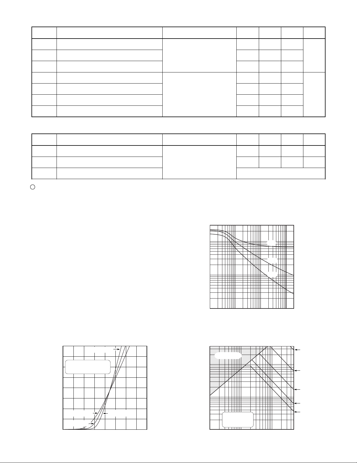
Figure 3, Typical Transfer Characteristics
FREQUENCY (MHz)
Figure 1, Typical Gain vs Frequency
TJ = -55°C
250µSEC. PULSE TEST
@ <0.5 % DUTY CYCLE
TJ = +125°C
, GATE-TO-SOURCE VOLTAGE (VOLTS)
TJ = -55°C
3000
1000
500
100
CAPACITANCE (pf)
50
10
.1 .5 1 5 10 50 200
VDS, DRAIN-TO-SOURCE VOLTAGE (VOLTS)
Figure 2, Typical Capacitance vs. Drain-to-Source Voltage
36
OPERATION HERE
LIMITED BY RDS (ON)
10
5
1
.5
, DRAIN CURRENT (AMPERES)
D
I
.1
Figure 4, Typical Maximum Safe Operating Area
TC =+25°C
TJ =+150°C
SINGLE PULSE
1 10 100 500
VDS, DRAIN-TO-SOURCE VOLTAGE (VOLTS)
C
iss
C
oss
C
rss
100uS
1mS
10mS
100mS
DC
Page 3

ARF463A/B
Note:
Duty Factor D =
t
1
/
t
2
Peak TJ = PDM x Z
θJC
+ T
C
t
1
t
2
P
DM
1.2
1.1
16
12
VGS=15V
10V
9V
1.0
0.9
(NORMALIZED)
, THRESHOLD VOLTAGE
0.8
GS(th)
V
0.7
-50 -25 0 25 50 75 100 125 150
Figure 5, Typical Threshold Voltage vs Temperature
160
120
80
, POWER OUT (WATTS)
40
OUT
P
TC, CASE TEMPERATURE (°C)
Class C
= 150V
V
DD
f = 81.36 MHz
0
0246810
Figure 7, Typical Power Out vs Power In
, POWER IN (WATTS)
P
IN
8
4
, DRAIN CURRENT (AMPERES)
D
I
0
1 5 10 15 20 25 30
, DRAIN-TO-SOURCE VOLTAGE (VOLTS)
V
DS
Figure 6, Typical Output Characteristics
14
12
10
(dB)
8
, COMMON SOURCE AMPLIFIER GAIN
PS
G
6
0 40 80 120 160
P
, POWER OUT (WATTS)
Figure 8, Typical Common Source Amplifier Gain vs Power Out
OUT
8V
7.5V
7V
6.5V
6V
5.5V
Class C
= 150V
V
DD
f = 81.36 MHz
0.8
0.1
0.05
0.01
0.005
, THERMAL IMPEDANCE (°C/W)
JC
q
Z
0.001
-5
10
D=0.5
0.2
0.1
0.05
PRELIMINARY
0.02
0.01
SINGLE PULSE
-4
10
Figure 9, Typical Maximum Effective Transient Thermal Impedance, Junction-To-Case vs Pulse Duration
-3
10
RECTANGULAR PULSE DURATION (SECONDS)
-2
10
-1
10
1.0 10
Table 1 - Typical Class AB Large Signal Input - Output Impedance
Freq. (MHz)
2.0
13.5
27
40
65
80
100
Zin - Gate shunted with 25Ω I
- Conjugate of optimum load for 100 Watts output at Vdd = 125V
Z
OL
Zin (Ω)
24 - j 5.0
7.8 - j 11
2.1 - j 6.4
.74 - j 3.3
.30 + j .42
.46 + j 2.0
.87 + j 3.7
= 50mA
DQ
(Ω)
Z
OL
55 - j 4.8
41 - j 24
23 - j 26.2
13.6 - j 22
6.1 - j 14.2
4.2 - j 10.7
2.7 - j 7.1
050-5998 Rev - 7-2001
Page 4

L4
ARF463A/B
Bias
0 - 12V
RF
Input
C2
C3
C7
L1
R2
R1
C1
L3
DUT
L2
C5
+
125V
-
C6
RF
C8
C4
Output
C5
81.36 MHz Test Circuit
C1 -- 820pF Unelco mounted at
gate lead
C2-C5 -- Arco 463 Mica trimmer
C5-C8 -- 10nF 500V COG chip
L1 -- 3t #18 .3" ID .25"L ~50nH
L2 -- 3t #16 AWG .25" ID .3"L ~58nH
L3 -- 10t #18 AWG .25 ID ~470nH
L4 -- VK200-4B ferrite choke ~3uH
R1-R2 -- 50 Ohm 1/2W Carbon
DUT = ARF463A/B
Source
TO-247 Package Outline
4.69 (.185)
5.31 (.209)
1.49 (.059)
2.49 (.098)
PRELIMINARY
6.15 (.242) BSC
20.80 (.819)
21.46 (.845)
4.50 (.177) Max.
0.40 (.016)
0.79 (.031)
19.81 (.780)
20.32 (.800)
1.01 (.040)
1.40 (.055)
Top View
15.49 (.610)
16.26 (.640)
5.38 (.212)
6.20 (.244)
3.55 (.138)
3.81 (.150)
2.87 (.113)
3.12 (.123)
1.65 (.065)
2.13 (.084)
Dimensions in Millimeters and (Inches)
NOTE: These two parts comprise a symmetric pair of RF
power transistors and meet the same electrical
specifications. The device pin-outs are the mirror image
of each other to allow ease of use as a push-pull pair.
Device
ARF - A
ARF - B
Gate Drain
Source Source
Drain Gate
2.21 (.087)
2.59 (.102)
5.45 (.215) BSC
2-Plcs.
APT's devices are covered by one or more of the following U.S.patents: 4,895,810 5,045,903 5,089,434 5,182,234 5,019,522 5,262,336
050-5998 Rev - 7-2001
5,256,583 4,748,103 5,283,202 5,231,474 5,434,095 5,528,058
 Loading...