

Page 1
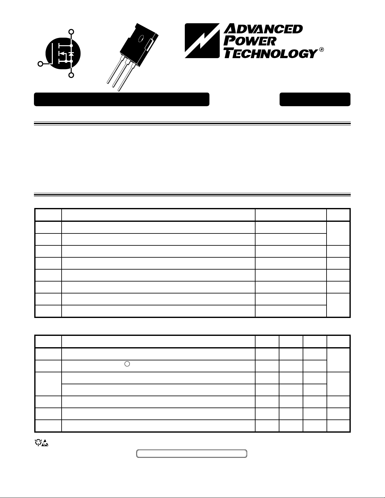
D
G
TO-247
ARF442 200W 100V 13.56MHz
S
RF OPERATION 1-15MHz
()
N-CH ANNEL ENHANCEMENT MODE RF POWER MOSFET
The ARF442 and ARF443 comprise a symmetric pair of RF power transistors designed for narrow-band push-pull
commercial, medical and industrial RF power amplifier applications.
• Specified 100 Volt, 13.56 MHz Characteristics:
• Output Power = 200 Watts.
• Gain = 22dB (Typ.)
• Efficiency = 73% (Typ.)
MAXIMUM RATINGS All Ratings: TC = 25°C unless otherwise specified.
Symbol
V
DSS
V
DGO
I
V
P
R
TJ,T
T
Parameter
Drain-Source Voltage
Drain-Gate Voltage
Continuous Drain Current @ T
D
Gate-Source Voltage
GS
Total Power Dissipation @ TC = 25°C
D
Junction to Case
θJC
Operating and Storage Junction Temperature Range
STG
Lead Temperature: 0.063" from Case for 10 Sec.
L
= 25°C
C
ARF443 200W 100V 13.56MHz
THE ARF442 PIN-OUTS ARE MIRROR IMAGE OF THE ARF443.
POWER MOS IV
• Low Cost Common Source RF Package.
• Very High Breakdown for Improved Ruggedness.
• Low Thermal Resistance.
• Nitride Passivated Die for Improved Reliability.
ARF442/443
300
300
8
±30
167
0.75
-55 to 150
300
®
UNIT
Volts
Amps
Volts
Watts
°C/W
°C
STATIC ELECTRICAL CHARACTERISTICS
Symbol
BV
VDS(ON)
I
DSS
I
GSS
g
VGS(TH)
USA
405 S.W. Columbia Street Bend, Oregon 97702-1035 Phone: (541) 382-8028 FAX: (541) 388-0364
EUROPE
Avenue J.F. Kennedy Bât B4 Parc Cadéra Nord F-33700 Merignac - France Phone: (33)557 92 15 15 FAX: (33) 556 47 9761
Characteristic / Test Conditions
Drain-Source Breakdown Voltage (V
DSS
On State Drain Voltage
Zero Gate Voltage Drain Current (V
Zero Gate Voltage Drain Current (V
Gate-Source Leakage Current (V
Forward Transconductance (VDS = 10V, ID = 5.5A)
fs
Gate Threshold Voltage (V
CAUTION: These Devices are Sensitive to Electrostatic Discharge. Proper Handling Procedures Should Be Followed.
1
(ID(ON) = 6.5A, VGS = 10V)
= VGS, ID = 50mA)
DS
APT Website - http://www.advancedpower.com
= 0V, ID = 250 µA)
GS
= V
DS
DSS
= 0.8 V
DS
= ±30V, V
GS
, VGS = 0V)
, VGS = 0V, TC = 125°C)
DSS
= 0V)
DS
MIN TYP MAX
300
250
1000
±100
3.5 4.5
25
UNIT
Volts
6
µA
nA
mhos
Volts
050-4506 Rev C
Page 2
DYNAMIC CHARACTERISTICS
ARF442/443
Symbol
C
C
C
Characteristic
Input Capacitance
iss
Output Capacitance
oss
Reverse Transfer Capacitance
rss
Test Conditions
V
= 0V
GS
VDS = 100V
f = 1 MHz
FUNCTIONAL CHARACTERISTICS
Symbol
G
η
G
η
1
Pulse Test: Pulse width < 380 µS, Duty Cycle < 2%
APT Reserves the right to change, without notice, the specifications and information contained herein.
Characteristic
Common Source Amplifier Power Gain
PS1
Drain Efficiency
1
ψ
Electrical Ruggedness VSWR 30:1
Common Source Amplifier Power Gain
PS2
Drain Efficiency
2
Test Conditions
= 100V
V
DD
= 0V
V
GS
P
= 200W
out
f = 13.56MHz
V
= 100V, P
DD
= 50mA, f = 13.56MHz
I
DQ
= 200W
out
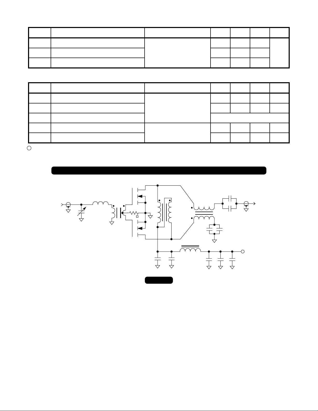
TYPICAL 13.56 MHz, 400 WATT PUSH-PULL CLASS 'C' POWER AMPLIFIER CIRCUIT
MIN TYP MAX
UNIT
730 900
100 140
pF
33 50
MIN TYP MAX
17 18.9
73
UNIT
dB
%
No Degradation in Output Power
22
65
dB
%
T1
2:1
R1
10K
RF
Input
C1
L1
75-480pF
0.5µH
C1 = 75-480pF Compression Mica
C2, C3, C4, C5, C6, C7 & C8 = .01µF @ 200V, CK06
C9 = .1µF @ 100V, CK06
C10 = 10µF @ 100V Electrolytic
R1 = 10KΩ, 5%, 1/4W, Carbon
Q1 = ARF442
Q2 = ARF443
L1 = 7.5 T of #18AWG, ID = .438", L = 0.5µH
Q1
Q2
BFC1
C6
.01µF
Parts List
.01µF
C2
T2
C3
.01µF
C4
C5
.01µF .01µF
RFC1
C7
.01µF
C8 C9 C10
.01µF .1µF 10µF (100V)
+
V
DD
RF
Output
= 100V
BFC1 = Balanced DC Feed Choke; 7 T of #22 stranded PTFE twisted pair on an Indiana General #F624-19-Q1 toroid. µi =125
RFC1 = 2 T of #18 stranded PTFE on a Fair-Rite #2677006301 shield bead. µi = 2000
T1 = 4:1 Z Conventional Transformer; 2:1 T of #22 stranded PTFE on a Fair-Rite #2843000202 Balun Core. µi = 850
T2 = 1:1 Z Transmission Line Transformer, using 50Ω coax.
• Coax = 22" of mini 50Ω PTFE coax, OD = .095"
• A large 2-hole balun core was constructed by gluing two Fair-Rite #2643102002, µi = 850 cores together.
• The transformer is constructed by winding 4.5 turns of the coax around the center of the balun core.
PCB = .062" G10 Epoxy Glass.
050-4506 Rev C
Page 3

ARF442/443
500
400
300
200
100
0
012345678910
16
12
Performance of aTypical
Push-Pull Power Amplifier (2-Devices)
f = 13.56 MHz
V
= 100V
DD
TJ = -55°C
VDS = 30V
250µSEC. PULSE TEST
@ <0.5 % DUTY CYCLE
RF POWER IN (WATTS)
Figure 1, RF Power Out vs RF Power In Figure 2, RF Power Out vs RF Power In
1.2
V
= V
DS
GS
1.1
8
4
, DRAIN CURRENT (AMPERES) RF POWER OUT (WATTS)
D
TJ = +125°C
TJ = +25°C
0
0 2 4 6 8 10 -50 -25 0 25 50 75 100 125 150
, GATE-TO-SOURCE VOLTAGE (VOLTS) TC, CASE TEMPERATURE (°C)
V
GS
Figure 2, Typical Transfer Characteristics Figure 3, Threshold Voltage vs Temperature
10
5
(ON)
DS
Operation Here
Limited By R
1
.5
TC =+25°C
, DRAIN CURRENT (AMPERES) I
D
TJ =+150°C
.1
1 5 10 50 100 300 -50 -25 0 25 50 75 100 125 150
V
, DRAIN-TO-SOURCE VOLTAGE (VOLTS) TJ, JUNCTION TEMPERATURE (°C)
DS
Figure 4, Maximum DC Safe Operating Area Figure 5, Breakdown Voltage vs Temperature
3,000
TJ = +25°C
TJ = +125°C
TJ = -55°C
1.0
0.9
(TH), THRESHOLD VOLTAGE
0.8
GS
0.7
1.2
1.1
1.0
0.9
VOLTAGE (NORMALIZED) (NORMALIZED)
0.8
(ON), DRAIN-TO-SOURCE BREAKDOWN V
DSS
0.7
BV
C
1,000
iss
500
C
oss
C
100
50
C, CAPACITANCE (pF) I
10
.01 .05 .1 .5 1 5 10 50 100
V
, DRAIN-TO-SOURCE VOLTAGE (VOLTS)
DS
Figure 6, Typical Capacitance vs. Drain-To-Source Voltage
rss
050-4506 Rev C
Page 4

Source
4.69 (.185)
5.31 (.209)
1.49 (.059)
2.49 (.098)
0.40 (.016)
0.79 (.031)
2.21 (.087)
2.59 (.102)
TO-247AD Package Outline
ARF442
15.49 (.610)
16.26 (.640)
6.15 (.242) BSC
20.80 (.819)
21.46 (.845)
ARF44E
4.50 (.177) Max.
19.81 (.780)
20.32 (.800)
Dimensions in Millimeters and (Inches)
1.01 (.040)
1.40 (.055)
5.45 (.215) BSC
2-Plcs.
5.38 (.212)
6.20 (.244)
3.55 (.138)
3.81 (.150)
2.87 (.113)
3.12 (.123)
1.65 (.065)
2.13 (.084)
GATE
SOURCE
DRAIN
ARF442/443
ARF443
4.69 (.185)
Source
5.31 (.209)
1.49 (.059)
2.49 (.098)
6.15 (.242) BSC
20.80 (.819)
21.46 (.845)
15.49 (.610)
16.26 (.640)
5.38 (.212)
6.20 (.244)
3.55 (.138)
3.81 (.150)
ARF44O
4.50 (.177) Max.
0.40 (.016)
0.79 (.031)
2.21 (.087)
2.59 (.102)
Dimensions in Millimeters and (Inches)
19.81 (.780)
20.32 (.800)
1.01 (.040)
1.40 (.055)
5.45 (.215) BSC
2-Plcs.
NOTE: The ARF442 and ARF443 comprise a symmetric pair of RF power transistors and
meet the same electrical specifications. The device pin-outs are the mirror image of each
other to allow ease of use as a push-pull pair.
2.87 (.113)
3.12 (.123)
1.65 (.065)
2.13 (.084)
DRAIN
SOURCE
GATE
CAUTION: These Devices are Sensitive to Electrostatic Discharge. Proper Handling Procedures Should Be Followed.
USA
405 S.W. Columbia Street Bend, Oregon 97702-1035 Phone:(541) 382-8028 FAX: (541) 388 -0364
EUROPE
Avenue J.F. Kennedy Bât B4 Parc Cadéra Nord F-33700 Merignac - France Phone: (33) 5 57 92 15 15 FAX: (33) 5 56 47 9761
050-4506 Rev C
 Loading...