

Page 1
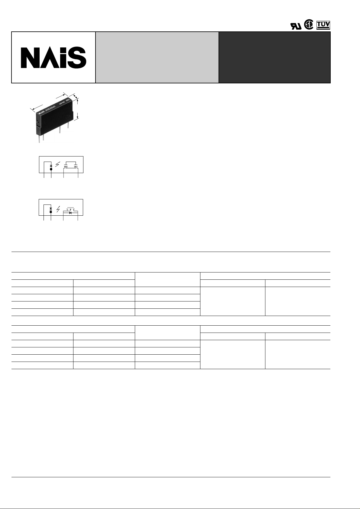
3.5±0.2
21±0.2
.827±.008
12 3 4
–+
AC/DC type
12 3 4
––++
DC type
.138±.008
12.5±0.2
.492±.008
POWER PhotoMOS RELAYS
(Voltage Sensitive Type)
FEATURES
1. A voltage sensitive power PhotoMOS relay
Conventional power PhotoMOS relays
are connected externally to an input limiting resistor in order to obtain the appropriate LED current. Adding an internal
mm inch
constant-current element renders the input limiting resistor unnecessary, making
it possible for the PhotoMOS relay to be
voltage driven.
2. Wide range of input voltages
Allows a wide range of input voltages from
4 to 30 V DC. The relay can be used in 5
V, 12 V or 24 V DC systems.
3. Large capacity PhotoMOS relay
Supports the various types of load control, from very small loads to a maximum
2.7 A for the AC/DC dual type, 3.6 A for
the DC-only type.
PhotoMOS
RELAYS
4. Both A C/DC dual types and DC-onl y
types are available
The AC/DC dual type is capable of bi-directional control, and unlike conventional
SSRs, does not have to be used diff erently depending on the load. The DC-only
type is well suited for control of DC solenoids and DC motors.
5. High sensitivity, low ON resistance
A maximum 3.6 A load can be controlled
with the minimum input voltage of 4 V DC.
The ON resistance is also low at 0.09 Ω
(AQZ102D).
6. Small scale, slim type, 4-pin SIL
Length 21.0 mm × width 3.5 mm × height
12.5 mm. High precision mounting is possible because of the small 73.5mm
of the 4-pin SIL.
2
area
TYPES
1. AC/DC type
Output rating
Load voltage Load current Inner carton Outer carton
60 V 2.7 A AQZ202D
100 V 1.8 A AQZ205D
200 V 0.9 A AQZ207D
400 V 0.45 A AQZ204D
2. DC type
Output rating
Load voltage Load current Inner carton Outer carton
60 V 3.6 A AQZ102D
100 V 2.3 A AQZ105D
200 V 1.1 A AQZ107D
400 V 0.6 A AQZ104D
Notes: Load voltage and current of AC/DC type: Peak AC/DC.
Load voltage and current of DC type: DC.
Part No.
25 pcs. 500 pcs.
Part No.
25 pcs. 500 pcs.
Packing quantity
Packing quantity
214
Page 2
°
°
°
°
°
°
°
°
RATING
1. AC/DC type
1) Absolute maximum ratings (Ambient temperature: 25 ° C 77 ° F)
Item Symbol AQZ202D AQZ205D AQZ207D AQZ204D Remarks
Input voltage V
Input
Input reverse voltage V
Power dissipation P
Load voltage (Peak AC) V
Output
Continuous load current (Peak AC) I
Peak load current I
Power dissipation P
Total power dissipation P
I/O isolation voltage V
T emperature
Operating T
limits
Storage T
2) Electrical characteristics (Ambient temperature: 25 ° C 77 ° F)
Item Symbol AQZ202D AQZ205D AQZ207D AQZ204D Remarks
Operate voltage
Input
Turn off voltage
Input current Typical I
On resistance
Output
Off state leakage current Maximum I
Turn on time*
Switching
speed
Turn off time*
Transfer
characteristics
I/O capacitance
Initial I/O isolation
resistance
Maximum operating
speed
Vibration resistance Minimum — 10 to 55 Hz at double amplitude of 3 mm 2 hours for 3 axes
Shock resistance Minimum — 4,900 m/s
Recommendable LED forward current I
*Turn on/off time
Typical
Maximum 4 V
Minimum
T ypical 1.3 V
Typical
Maximum 0.18 Ω
Typical
Maximum 10.0 ms
Typical
Maximum 3.0 ms
Typical
Maximum 1.5 pF
Minimum R
Maximum — 0.5 cps
= 5 to 10 mA. For type of connection, see page 35.
F
IN
RIN
in
L
L
peak
out
T
iso
–40 ° C to +85 ° C –40 ° F to +185 ° F (4 V
–40 ° C to +75 ° C –40 ° F to +167 ° F (6 V < V
opr
–40 ° C to +60 ° C –40 ° F to +140 ° F (15 V < V
stg
V
Fon
V
Foff
IN
R
leak
T
T
0.066 Ω
on
5.8 ms 4.2 ms 2.7 ms 2.3 ms
on
0.2 ms 0.2 ms 0.1 ms 0.1 ms
off
Ciso
iso 1,000 MΩ 500 V DC
AQZ10 ❍ D, 20 ❍ D
30 V
3 V
300 mW
60 V 100 V 200 V 400 V
2.7 A 1.8 A 0.9 A 0.45 A
9.0 A 6.0 A 3.0 A 1.5 A 100 ms (1 shot), V
1.6 W
1.6 W
2,500 V AC
q
V
q
6 V)
–40 ° C to +100 ° C –40 ° F to +212 ° F
1.4 V
0.8 V
6.5 mA V
0.180 Ω
0.34 Ω
0.64 Ω
1.1 Ω
10 µ A
0.8 pF
2
{500 G}1 ms 3 times for 3 axes
IN
IN
IN
2.4 Ω
3.2 Ω
q
15 V)
q
30 V)
Non-condensing at low
temperatures
I
L
= 100 mA
V
L
= 10 V
I
L
= 100 mA
V
L
= 10 V
= 5 V
IN
V
= 5 V
IN
I
= Max.
L
Within 1 s on time
= 0
IN
V
V
= Max.
L
V
= 5 V
IN
I
= 100 mA
L
V
= 10 V
L
V
= 5 V
IN
I
L = 100 mA
VL= 10 V
f = 1 MHz
V
B = 0
V
IN= 5 V
Duty factor = 50%
IL×VL = 200 (VA)
= DC
L
Input
Output 10%
Ton
Toff
90%
2. DC type
1) Absolute maximum ratings (Ambient temperature: 25 ° C 77 ° F)
Item Symbol AQZ102D AQZ105D AQZ107D AQZ104D Remarks
IN
RIN
in
L
L
peak
out
T
iso
–40
–40
opr
–40 ° C to +60 ° C –40 ° F to +140 ° F (15 V < V
stg
Input
Output
T emperature
limits
Input voltage V
Input reverse voltage V
Power dissipation P
Load voltage (DC) V
Continuous load current (DC) I
Peak load current I
Power dissipation P
Total power dissipation P
I/O isolation voltage V
Operating T
Storage T
30 V
3 V
300 mW
60 V 100 V 200 V 400 V
3.6 A 2.3 A 1.1 A 0.6 A
9.0 A 6.0 A 3.0 A 1.5 A 100 ms (1 shot), V
1.35 W
1.35 W
2,500 V AC
q
V
C to +85
C to +75
C –40
C –40
F to +185
F to +167
F (4 V
F (6 V < V
IN
IN
IN
q
6 V)
q
15 V)
q
30 V)
Non-condensing at low
temperatures
–40 ° C to +100 ° C –40 ° F to +212 ° F
L
= DC
215
Page 3

AQZ10❍D, 20❍D
2) Electrical characteristics (Ambient temperature: 25°C 77°F)
Item Symbol AQZ102D AQZ105D AQZ107D AQZ104D Remarks
Typical
Maximum 4 V
Minimum
T ypical 1.3 V
VFon
VFoff
Input
Operate voltage
Turn off voltage
Input current Typical IIN 6.5 mA VIN = 5 V
Output
On resistance
Typical
Maximum 0.09 Ω 0.17 Ω 0.55 Ω 1.6 Ω
Ron
0.033 Ω 0.090 Ω 0.33 Ω 1.23 Ω
Off state leakage current Maximum Ileak 10 µA
Transfer
characteristics
Turn on time*
Switching
speed
Turn off time*
I/O capacitance
Initial I/O isolation
resistance
Maximum operating
speed
Typical
Maximum 10.0 ms
Typical
Maximum 3.0 ms
Typical
Maximum 1.5 pF
Ton
T
Ciso
Minimum Riso 1,000 MΩ 500 V DC
Maximum — 0.5 cps
3.3 ms 2.2 ms 1.5 ms 1.2 ms
0.2 ms 0.2 ms 0.1 ms 0.1 ms
off
Vibration resistance Minimum — 10 to 55 Hz at double amplitude of 3 mm 2 hours for 3 axes
Shock resistance Minimum — 4,900 m/s2 {500 G}1 ms 3 times for 3 axes
Recommendable LED forward current IF = 5 to 10 mA. For type of connection, see page 35.
*Turn on/off time
1.4 V
0.8 V
0.8 pF
IL = 100 mA
VL = 10 V
IL = 100 mA
VL = 10 V
VIN = 5 V
IL = Max.
Within 1 s on time
VIN = 0
VL = Max.
VIN = 5 V
IL = 100 mA
L = 10 V
V
VIN = 5 V
IL = 100 mA
L= 10 V
V
f = 1 MHz
VB = 0
VIN= 5 V
Duty factor = 50%
IL×VL = 200 (VA)
Input
Output 10%
Ton
Toff
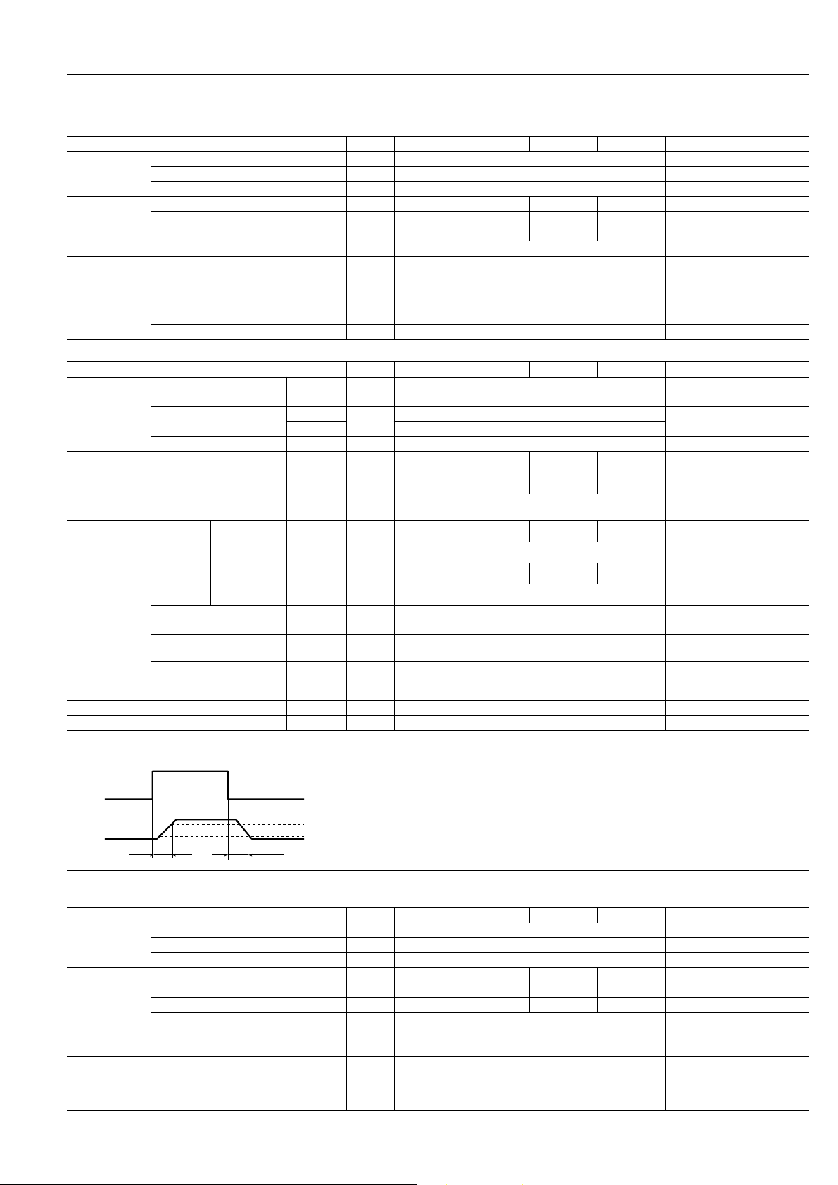
REFERENCE DATA
1. Load current vs. ambient temperature characteristics
Allowable ambient temperature: –40°C to +85°C
IN: Input voltage; IL (derate):Load current (derate); I L:
V
Absolute maximum ratings of continuous load current
120
100
80
× 100, %
60
L
I
(derate)
L
I
40
20
–40°F to +185°F;
4V VIN 6V
6V<VIN 15V
15V<VIN 30V
90%
■ For Dimensions, see Page 29.
■ For Schematic and Wiring Diagrams, see Page 35.
■ For Cautions for Use, see Page 40.
2.-(1) Load current vs. ambient temperature
characteristics in adjacent mounting
Input voltage: 4V q VIN q 6V;
L (derate): Load current (derate); IL: Absolute maxi-
I
mum ratings of continuous load current; : Adjacent
mounting pitch
100
=20mm
80
× 100, %
60
L
I
(derate)
40
L
I
20
=10mm
= 5mm
2.-(2) Load current vs. ambient temperature
characteristics in adjacent mounting
Input voltage: 6V < VIN q 15V;
L (derate): Load current (derate); IL: Absolute maxi-
I
mum ratings of continuous load current; : Adjacent
mounting pitch
100
80
× 100, %
60
L
I
(derate)
L
40
I
20
=20mm
=10mm
= 5mm
216
0
02040600–20
Ambient temperature, °C
80
100–40
85
0
02040600–20
Ambient temperature, °C
80
100–40
85
0
02040600–20
Ambient temperature, °C
80
100–40
75
Page 4

2.-(3) Load current vs. ambient temperature
characteristics in adjacent mounting
Input voltage: 15V<VIN q 30V;
L (derate): Load current (derate); IL: Absolute maxi-
I
mum ratings of continuous load current; : Adjacent
mounting pitch
100
3.-(1) On resistance vs. ambient temperature
characteristics (AC/DC type)
Input voltage: 5 V;
Continuous load current: 2.7 A (DC) (AQZ202D)
1.8 A (DC) (AQZ205D)
0.5
AQZ10❍D, 20❍D
3.-(2) On resistance vs. ambient temperature
characteristics (AC/DC type)
Input voltage: 5 V;
Continuous load current: 0.9 A (DC) (AQZ207D)
0.45 A (DC) (AQZ204D)
5.0
80
× 100, %
60
L
I
(derate)
40
L
I
20
0
0204060–20 80 100–40
Ambient temperature, °C
=20mm
=10mm
= 5mm
3.-(3) On resistance vs. ambient temperature
characteristics (DC type)
Input voltage: 5 V;
Continuous load current: 3.6 A (DC) (AQZ102D)
0.25
0.20
0.15
0.10
On resistance, Ω
0.05
0
–40
2.3 A (DC) (AQZ105D)
AQZ105D
AQZ102D
0–20 20 40 60
Ambient temperature, °C
80
85
0.4
0.3
0.2
On resistance, Ω
0.1
0
–40
AQZ205D
AQZ202D
0–20 20 40 60
Ambient temperature, °C
80
85
3.-(4) On resistance vs. ambient temperature
characteristics (DC type)
Input voltage: 5 V;
Continuous load current: 1.1 A (DC) (AQZ107D)
5.0
4.0
3.0
2.0
On resistance, Ω
1.0
0
–40
0.6 A (DC) (AQZ104D)
AQZ104D
AQZ107D
0–20 20 40 60
Ambient temperature, °C
80
85
4.0
3.0
2.0
On resistance, Ω
1.0
0
–40
AQZ204D
AQZ207D
0–20 20 40 60
Ambient temperature, °C
80
85
4.-(1) Turn on time vs. ambient temperature
characteristics (AC/DC type)
Input voltage: 5 V;
Load voltage: 10 V (DC);
Continuous load current: 100 mA (DC)
10
8
6
4
Turn on time, ms
2
0
–40
AQZ202D
AQZ205D
AQZ207D
AQZ204D
0–20 20 40 60 80
Ambient temperature, °C
85
4.-(2) Turn on time vs. ambient temperature
characteristics (DC type)
Input voltage: 5 V; Load voltage: 10 V (DC);
Continuous load current: 100 mA (DC)
10
8
6
4
Turn on time, ms
2
0
–40
Ambient temperature, °C
AQZ102D
AQZ105D
AQZ107D
AQZ104D
00–20 20 40 60
80
85
6. Operate voltage vs. ambient temperature
characteristics
Load voltage: 10 V (DC);
Continuous load current: 100 mA (DC)
5.0
4.0
3.0
2.0
Operate voltage, V
1.0
5.-(1) Turn off time vs. ambient temperature
characteristics (AC/DC type)
Input voltage: 5 V; Load voltage: 10 V (DC);
Continuous load current: 100 mA (DC)
0.5
0.4
0.3
0.2
Turn off time, ms
0.1
AQZ204D
AQZ207D
0
–40 0–20 20 40 60 80
Ambient temperature, °C
AQZ202D
AQZ205D
85
7. Turn off voltage vs. ambient temperature
characteristics
Load voltage: 10 V (DC);
Continuous load current: 100 mA (DC)
5.0
4.0
3.0
2.0
Turn off voltage, ms
1.0
5.-(2) Turn off time vs. ambient temperature
characteristics (DC type)
Input voltage: 5 V; Load voltage: 10 V (DC);
Continuous load current: 100 mA (DC)
0.5
0.4
0.3
AQZ107D
0.2
Turn off time, ms
0.1
AQZ104D
0
–40 0–20 20 40 60 80
Ambient temperature, °C
AQZ102D
AQZ105D
85
8. Input current vs. ambient temperature characteristics
Input voltage: 5 V
10
8
6
4
Input current, mA
2
0
–40
0–20 20 40 60
Ambient temperature, °C
80
85
0
–40
0–20 20 40 60
Ambient temperature, °C
80
85
0
–40
0–20 20 40 60
Ambient temperature, °C
80
85
217
Page 5

AQZ10❍D, 20❍D
9.-(1) Voltage vs. current characteristics of output at MOS portion (AC/DC type)
Ambient temperature: 25°C 77°F
4.0
AQZ202D
3.0
AQZ205D
2.0
AQZ207D
Current, A
1.0
–2.0 –1.5 –1.0 –0.5
0 2.01.51.00.5
–1.0
–2.0
–3.0
–4.0
AQZ204D
Voltage, V
9.-(2) Voltage vs. current characteristics of output at MOS portion (DC type)
Ambient temperature: 25°C 77°F
4.0
AQZ102D
3.0
AQZ105D
–0.8 –0.6 –0.4 –0.2
2.0
Current, A
1.0
0 0.80.60.40.2
–1.0
–2.0
–3.0
–4.0
AQZ107D
AQZ104D
Voltage, V
10. Input voltage vs. input current characteristics
Ambient temperature: 25°C 77°F
10
8
6
4
Input current, mA
2
0
0 5 10 15 20
Input voltage, V
25 30
11.-(1) Off state leakage current
Ambient temperature: 25°C 77°F
–3
10
–6
10
–9
10
Off state leakage current, A
10
–12
0
AQZ105D,205D
AQZ102D,202D
50 100
Load voltage, V
13.-(1) Applied voltage vs. output capacitance
characteristics (AC/DC type)
Frequency: 1 MHz; Ambient temperature: 25°C 77°F
2000
1800
1600
1400
1200
1000
800
Output capacitance, pF
600
400
200
0
AQZ202D
AQZ205D AQZ207D
AQZ204D
20 40 60 80 1000
Applied voltage, V
11.-(2) Off state leakage current
Ambient temperature: 25°C 77°F
–3
10
–6
10
–9
10
Off state leakage current, A
–12
10
0
AQZ104D,204D
AQZ107D,207D
50 100
Load voltage, V
13.-(2) Applied voltage vs. output capacitance
characteristics (DC type)
Frequency: 1 MHz; Ambient temperature: 25°C 77°F
2000
1800
1600
1400
1200
AQZ102D
1000
800
600
400
200
AQZ105D
AQZ107D
AQZ104D
0
20 40 60 80 1000
Applied voltage, V
Output capacitance, pF
12. Maximum operating speed vs . load voltage
× load current characteristics
Input voltage: 5V; Ambient temperature: 25°C 77°F
10
9
8
7
6
5
4
3
Maximum operating speed, cps
2
1
0
0 25 50 75 175
Maximum voltage, V×Load current, A
100 125 150 200
duty=50%
5.08
.200
5.08
.200
mm inch
2-1.2 dia.
2-.047 dia.
±0.05 dia.
2-1.2
±002 dia.
2-.047
ACCESSORY
Socket
12 345 6
4
.157
5/7/2001 All Rights Reserved, © Copyright Matsushita Electric Works, Ltd.
218
22.6
.890
0.5
.020
2.54
.100
6.35
.250
PA1a-PS
±0.6
±.024
0.8
.031
3.81
.150
(0.3)
(.012)
5.08
.200
.197
9
.354
5.3
.209
+0.2
5
–0.6
±.008
–.024
±0.6
±.024
±0.6
±.024
0.25
.010
1.23
.048
.039
±0.25
1
1.23
.048
±.010
12 345 6
3.9
.154
.020
6.35
.250
0.5
2.54
.100
22.6
.890
±0.6
±.024
0.8
.031
PA1a-PS-H
3.81
.150
5.08
.200
5
.197
9
.354
5.3
.209
(0.3)
(.012)
+0.2
–0.6
±.008
–.024
±0.6
±.024
±0.6
±.024
±0.15
1.3
±.006
.051
PC board pattern
(BOTTOM VIEW)
Standard type
2.54
.100
10.16
.400
2-1 dia.
2-.039 dia.
Self clinching type
2.54
.100
2-0.8
2-.031
10.16
.400
±0.25 dia.
±002 dia.
Tolerance: ±0.1 ±.004
Go To Online Catalog
 Loading...