

Page 1
AQY221❍2S
UL
pending
CSA
pending
4.3
.169
4.4
.173
2.1
.083
4.3
.169
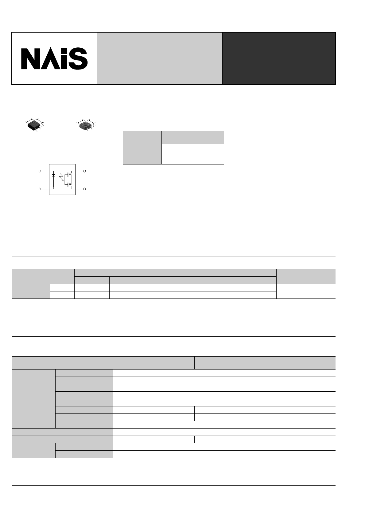
<R type> <C type>
mm inch
1
2
4
3
4.4
.173
2.1
.083
RF (Radio Frequency)
C ✕ R 10 Type
(by)
FEATURES
1. Two option package available.
R type offers greatly reduced onresistance.
C type offers lower output capacitance.
Ω
AQY221N2S
(C type)
9.5
AQY221R2S
(R type)
Output
capacitance: C
On resistance: R 0.8
13pF 1pF
2. High speed switching
Turn on time: 30µs (AQY221N2S)
Turn off time: 30µs (AQY221N2S)
3. Super miniature design
SOP 4-pin type.
4. Low-level off state leakage current
of 10pA
The SSR has an off state leakage current
of several milliamperes, where as this
PhotoMOS relay has only 10pA (typical)
even with the rated load voltage
(AQY221N2S)
PhotoMOS
RELAYS
TYPICAL
APPLICATIONS
Measuring and testing equipment
1. Testing equipment for
semiconductor performance
IC tester, Liquid crystal driver tester , semiconductor performance tester
2. Board tester
Ω
Bare board tester, In-circuit tester, function tester
3. Medical equipment
Ultrasonic wave diagnostic machine
4. Multi-point recorder
Warping, thermo couple
TYPES
Circuit
arrangement
1 Form A
Type
R type 40 V 250 mA AQY221R2SX AQY221R2SZ
C type 40 V 120 mA AQY221N2SX AQY221N2SZ
* Indicate the peak AC and DC values.
Notes:
(1) Tape package is the standard packing style. Also available in tube.
(Part No. suffix "X" or "Z" is not needed when ordering; Tube: 100 pcs.; Case: 2,000 pcs.)
(2) For space reasons, the initial letters of the product number "AQY and S", the package type indicator "X" and "Z" are omitted from the seal.
Output rating* Tape and reel packing style
Load voltage Load current Picked from the 1/2-pin side Picked from the 3/4-pin side
Packing quantity
Tape and reel: 1,000 pcs.
RATING
1. Absolute maximum ratings (Ambient temperature: 25°C 77°F)
Item
LED forward current I
Input
Output
Total power dissipation P
I/O isolation voltage V
Temperature limits
LED reverse voltage V
Peak forward current I
Power dissipation P
Load voltage (peak AC) V
Continuous load current I
Peak load current I
Power dissipation P
Operating T
Storage T
Symbol
peak
AQY221R2S
(R type)
F
R
FP
in
L
L
out
T
iso
opr
stg
0.25A 0.12A Peak AC,DC
0.75A 0.30A 100 ms (1 shot), VL= DC
500V AC 1,500V AC
–40°C to +85°C –40°F to +185°F Non-condensing at low temperatures
–40°C to +100°C –40°F to +212°F
50mA
75mW
40V
300mW
350mW
AQY221N2S
(C type)
3V
1A f=100 Hz, Duty factor=0.1%
Remarks
2
Page 2
2. Electrical characteristics (Ambient temperature: 25°C 77°F)
Item Symbol
LED operate current
Input
LED turn off current
LED dropout voltage
On resistance
Output
Output capacitance
Off state leakage current
Turn on time*
Switching
speed
Transfer
characteristics
Turn off time*
I/O capacitance
Initial I/O isolation resistance Minimum R
Note: Recommendable LED forward current IF = 5 mA.
For type of connection, see Page 6
Typical
Maximum 3.0 mA
Minimum
Typical 0.4 mA 0.85 mA
Typical
Maximum 1.5 V
I
Fon
I
Foff
V
F
Typical
R
Maximum 1.25
on
Typical
C
I
out
Leak
Maximum 18 pF 1.5 pF
Typical
Maximum 10 nA
Typical
T
Maximum 0.5ms
on
Typical
T
Maximum 0.2 ms
Typical
Maximum 1.5 pF
off
C
iso
iso
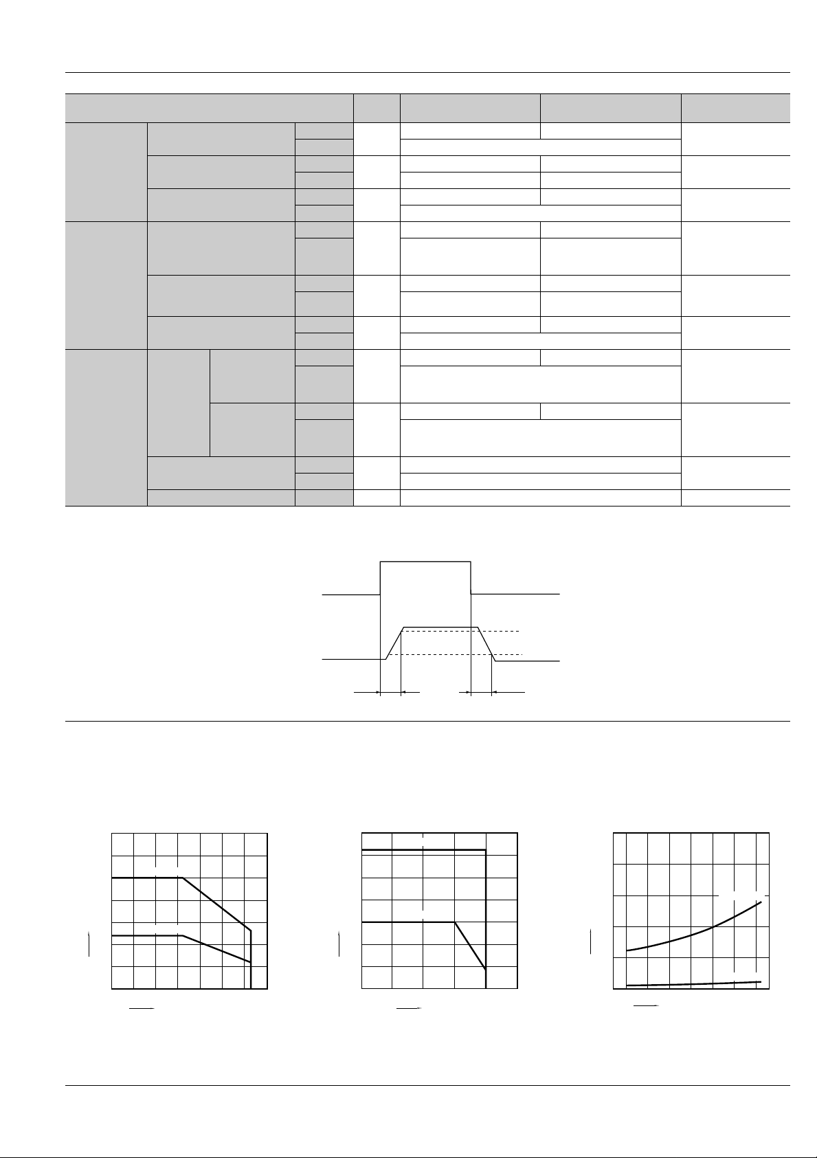
*Turn on/Turn off time
AQY221❍2S
AQY221R2S
(R type)
0.5 mA 0.9 mA
0.1 mA 0.2 mA
1.14 V(1.25 V at IF = 50mA) 1.14 V(1.25 V at IF = 50mA)
0.8
Ω
Ω
13 pF 1.0 pF IF = 0
0.03 nA 0.01 nA
0.1 ms 0.03 ms IF = 5mA
0.06ms 0.03ms IF = 5mA
0.8 pF
1,000M
AQY221N2S
Ω
(C type)
9.5
Ω
12.5
Ω
Condition
IL = 250 mA (R type)
IL = 80 mA (C type)
IL = 250 mA (R type)
IL = 80 mA (C type)
IF = 5mA
IF = 5mA
IL = 250 mA (R type),
IL = 80 mA (C type)
Within 1 s on time
VB = 0 V
f = 1 MHz
IF = 0
VL = Max.
VL = 10V
RL = 40Ω (R type),
125Ω (C type)
VL = 10V
RL = 40Ω (R type),
125Ω (C type)
f = 1MHz
VB = 0
500V DC
REFERENCE DATA
1. Load current vs. ambient temperature
characteristics
Allowable ambient temperature: –40°C to +85°C
350
300
250
200
150
Load current, mA
100
AQY221R2S
AQY221N2S
50
0
0204060
Ambient temperature, °C
–40°F to +185°F
8085
Input
90%
Toff
10%
3. On resistance vs. ambient temperature
characteristics
Measured portion: between terminals 3 and 4
LED current: 5 mA; Load voltage: Max. (DC);
Load current: 250mA (DC) [R type], 80mA (DC)
[C type];
25
20
15
On resistance, Ω
10
5
0
02040608085-40 -20
Ambient temperature, °C
AQY221N2S
AQY221R2S
Output
Ton
2. Load current vs. Load voltage characteristics
Ambient temperature: 25°C 77°F
280
240
200
160
120
Load current, mA
80
40
100-40 -20
AQY221R2S
AQY221N2S
0
10 20 30 40 500
Load voltage, V
3
Page 3

AQY221❍2S
4. Turn on time vs. ambient temperature
characteristics
Measured portion: between terminals 3 and 4
LED current: 5 mA; Load voltage: 10V (DC);
Continuous load current: 250mA (DC) [R type], 80mA
(DC) [C type];
0.3
0.25
0.2
0.15
Turn on time, ms
0.1
0.05
AQY221R2S
AQY221N2S
5. Turn off time vs. ambient temperature
characteristics
LED current: 5 mA; Load voltage: 10V (DC);
Continuous load current: 250mA (DC) [R type], 80mA
(DC) [C type];
0.1
0.08
0.06
Turn off time, ms
0.04
0.02
AQY221R2S
AQY221N2S
6. LED operate current vs. ambient
temperature characteristics
Load voltage: Max. (DC);
Continuous load current: 250mA (DC) [R type], 80mA
(DC) [C type];
2
AQY221N2S
1.5
1
LED operate current, mA
0.5
AQY221R2S
0
-40 -20
0204060
Ambient temperature, °C
80
85
7. LED turn off current vs. ambient temperature
characteristics
Load voltage: Max. (DC);
Continuous load current: 250mA (DC) [R type], 80mA
(DC) [C type];
2
AQY221N2S
1.5
1
LED turn off current, mA
0.5
0
-40 -20
0204060
Ambient temperature, °C
AQY221R2S
8085
10. Off state leakage current
Measured portion: between terminals 3 and 4
Ambient temperature: 25°C 77°F
-3
10
-6
10
-9
10
Off state leakage current, A
-12
10
050
AQY221R2S
AQY221N2S
Load voltage, V
40302010
13. Applied voltage vs. output capacitance
characteristics
Measured portion: between terminals 3 and 4
Frequency: 1 MHz, 30m Vrms; Ambient temperature:
25°C 77°F
30
25
20
15
10
Output capacitance, pF
5
0
0
AQY221R2S
AQY221N2S
2010 30 40 50
Applied voltage, V
4
0
-40 -20
0204060
Ambient temperature, °C
8085
8. LED dropout voltage vs. ambient
temperature characteristics
LED current: 5 to 50 mA
1.5
1.4
1.3
1.2
LED dropout voltage, V
1.1
1.0
0
-40 -20 0204060
Ambient temperature, °C
50mA
30mA
20mA
10mA
5mA
80
85
100
11. LED forward current vs. turn on time
characteristics
Measured portion: between terminals 3 and 4
Load voltage: 10V (DC);
Continuous load current: 250mA (DC) [R type], 80mA
(DC) [C type];
Ambient temperature: 25°C 77°F
0.3
0.25
0.2
0.15
Turn on time, ms
0.1
0.05
AQY221R2S
AQY221N2S
0
100203040
LED forward current, mA
50 60
14. Isolation characteristics
(50Ω impedance)
Measured portion: between terminals 3 and 4
Ambient temperature: 25°C 77°F
100
80
60
Isolation, dB
40
20
0
45
10
10 10 10
AQY221N2S
AQY221R2S
68
7
Frequency, Hz
10
0
-40 -20
0204060
Ambient temperature, °C
8085
9. Voltage vs. current characteristics of output
at MOS portion
Measured portion: between terminals 3 and 4
Ambient temperature: 25°C 77°F
300
AQY221R2S
200
-3.0
-2.5
-2.0
-1.5
-1.0
-0.5
Current, mA
100
0.5
-100
-200
-300
AQY221N2S
1,0
1.5
2.0
Voltage, V
2.5
3.0
12. LED forward current vs. turn off time
characteristics
Measured portion: between terminals 3 and 4
Load voltage: 10V (DC);
Continuous load current: 250mA (DC) [R type], 80mA
(DC) [C type];
Ambient temperature: 25°C 77°F
0.1
0.08
0.06
Turn off time, ms
0.04
AQY221R2S
0.02
0
100203040
AQY221N2S
LED forward current, mA
50 60
15. Insertion loss characteristics
(50Ω impedance)
Measured portion: between terminals 3 and 4
Ambient temperature: 25°C 77°F
2
1.5
1
Insertion loss, dB
0.5
0
45
10
AQY221N2S
AQY221R2S
10 10 10
Frequency, Hz
67
Page 4

16-(1). On resistance distribution (R type)
Measured portion: between terminals 3 and 4
Continuous load current: 250mA (DC)
Ambient temperature: 25°C 77°F
60
50
16-(2). On resistance distribution (C type)
Measured portion: between terminals 3 and 4
Continuous load current: 80mA (DC)
Ambient temperature: 25°C 77°F
60
50
AQY221❍2S
17-(1). Turn on time distribution (R type)
Load voltage: 10V (DC)
Continuous load current: 250mA (DC)
Ambient temperature: 25°C 77°F
60
50
40
30
Quantity, n
20
10
0
0.76 0.77 0.790.78 0.8 0.810.82 0.83 0.84 0.85 0.84
On resistance, Ω
17-(2). Turn on time distribution (C type)
Load voltage: 10V (DC)
Continuous load current: 80mA (DC)
Ambient temperature: 25°C 77°F
60
50
40
30
Quantity, n
20
10
0
0.01 0.02 0.03 0.04 0.060.05
Turn on time, ms
40
30
Quantity, n
20
10
0
8.6 9 9.4 9.8 10.2 10.6
On resistance, Ω
18-(1). Turn off time distribution (R type)
Load voltage: 10V (DC)
Continuous load current: 250mA (DC)
Ambient temperature: 25°C 77°F
60
50
40
30
Quantity, n
20
10
0
0.022 0.0240.023 0.0260.025 0.027 0.028 0.029 0.03 0.031 0.032
Turn off time, ms
40
30
Quantity, n
20
10
0
0.09 0.1 0.11 0.12 0.13 0.14 0.15 0.16 0.17 0.18 0.19
Turn on time, ms
18-(2). Turn off time distribution (C type)
Load voltage: 10V (DC)
Continuous load current: 80mA (DC)
Ambient temperature: 25°C 77°F
60
50
40
30
Quantity, n
20
10
0
0.018 0.022 0.026 0.03 0.034 0.038
Turn off time, ms
19-(1). LED operate current distribution
(R type)
Load voltage: 10V (DC)
Continuous load current: 250mA (DC)
Ambient temperature: 25°C 77°F
60
50
40
30
Quantity, n
20
10
0
0.7 0.8 0.9 1 1.1 1.2
LED operate current, mA
DIMENSIONS
19-(2). LED operate current distribution
(C type)
Load voltage: 10V (DC)
Continuous load current: 80mA (DC)
Ambient temperature: 25°C 77°F
60
50
40
30
Quantity, n
20
10
0
.016
0.4
4.3±0.2
.169±.009
2.54
.100
0.4 0.6 0.8 1 1.2 1.4
4.4±0.2
.173±009
2.0±0.2
.079±.009
0.1
.004
0.4
.016
LED operate current, mA
0.5
.020
6.8±0.4
.268±016
0.5
.020
Terminal thickness = 0.15 .006
General tolerance: ±0.1 ±.004
Recommended mounting pad (TOP VIEW)
6.0
.236
1.2
.047
0.8
.032
2.54
.100
Tolerance:±0.1 ±.004
mm inch
5
Page 5

AQY221❍2S
SCHEMATIC AND WIRING DIAGRAMS
• E1: Power source at input side; VIN: Input voltage; IF: LED forward current; IIN: Input current; VL: Load voltage; IL: Load current
Output
configuration
1
Schematic
4
1a AC/DC
2
3
CAUTIONS FOR USE
1. Short across terminals
Do not short circuit between terminals
when relay is energized. There is possibility of breaking the internal IC.
2. Surge voltages at the input
If reverse surge voltages are present at
the input terminals, connect a diode in reverse parallel across the input terminals
and keep the reverse voltages below the
reverse breakdown voltage.
1
2
3. Recommended LED forwar d current
(I
F
)
It is recommended that the LED forward
current (IF) be kept at 5mA.
4. Ripple in the input power supply
If ripple is present in the input power supply, observe the following:
1) For LED operate current at E
tain the value mentioned in the table of
“Note 3. Recommended LED forward current (I
F
).”
2) Keep the LED operate current at 50
mA or less at E
max.
Emin. Emax.
min,
4
3
main-
Load Wiring diagram
1
E1
I
F
2
5. Output spike voltages
1) If an inductive load generates spike
voltages which exceed the absolute maximum rating, the spike voltage must be
4
I
VL (AC,DC)
3
L
Load
Cleaning solvent
Chlorine
base
limited.
Typical circuits are shown below.
1
2
1
4
3
4
Load
Add a clamp diode
to the load
Adueous
Alcohol
base
Others
7. Input wiring pattern
This relays, avoid installing the input
(LED side) wiring pattern to the bottom
side of the package if you require the
specified I/O isolation voltage (V
2
3
Load
Add a CR snubber
circuit to the load
mounting the PC board. Since part of the
frame on the output side is exposed, it
may cause fluctuations in the I/O isolation
voltage.
2) If spike voltages generated at the load
are limited with a clamp diode and the circuit wires are long, spike voltages will occur by inductance. Keep wires as short
as possible to minimize inductance.
6. Cleaning solvents compatibility
Dip cleaning with an organic solvent is
recommended for removal of solder flux,
dust, etc. Select a cleaning solvent from
the following table. If ultrasonic cleaning
is used, the severity of factors such as
frequency, output power and cleaning
solvent selected may cause loose wires
and other defects. Make sure these conditions are correct before use. F or details,
please consult us.
Load
4
VL (AC,DC)
I
3
L
Compatibility
(❍: Yes ✕: No)
• T richlene
• Chloroethlene
❍
• Indusco
• Hollis
❍
• Lonco Terg
• IPA
• Ethanol
• Thinner
• Gasoline
Portion of output side frame
(Output
terminal side)
Input wiring
pattem
May not allow the prescribed I/O withstand
voltage (Viso) to be achieved
(Input terminal
side)
❍
✕
) after
iso
6
Page 6

AQY221❍2S
21±0.8
.827±.031
80±1 dia.
3.150±.039 dia.
2±0.5
.079±.020
13±0.5 dia.
.512±.020 dia.
14±1.5
.551±.059
2±0.5
.079±.020
250±2 dia.
9.843±.079 dia.
80±1 dia.
3.150±.039 dia.
8. Soldering
When soldering this terminals, the following conditions are recommended.
(1) IR (Infrared reflow) soldering method (2) Vapor phase soldering method (3) Double wave soldering method
T3
T2
T1
T2
T1
T2
T1
t1 t2
T1 = 155 to 165°C 311 to 329°F
T2 = 180°C 200°C 356 to 392°F
T3 = 245°C 473°F or less
t1 = 120 s or less
t2 = 30 s or less
(4) Soldering iron method
Tip temperature: 280 to 300°C 536 to
572 °F
Wattage: 30 to 60 W
Soldering time: within 5 s
(5) Others
Check mounting conditions before using
other soldering methods (hot-air, hot
plate, pulse heater, etc.)
• The temperature profile indicates the
temperature of the soldered terminal on
the surface of the PC board. The ambient
t1 t2
T1 = 180 to 200°C 366 to 392°F
T2 = 215°C 419°F or less
t1 = 40 s
t2 = 40 s or less
T1 = 155 to 165°C 311 to 329°F
T2 = 260°C 500°F or less
t1 = 60 s or less
t2+t3 = 5 s or less
temperature may increase excessively.
Check the temperature under mounting
conditions.
• The conditions for the infrared reflow
soldering apply when preheating using
the VPS method.
9. The following shows the packaging format
1) Tape and reel
Type Tape dimensions Dimensions of paper tape reel
Direction of picking
12±0.3
.472±.012
7.2±0.1
.284±.004
4±0.1
.157±.004
2±0.1
.079±.004
❍❍❍
1.75±0.1
.069±.004
5.5±0.1
±
.004
.217
±
0.1
4.7
12±0.1
±
.004
.185
.472±.004
1.55±0.1 dia.
.061±.004 dia.
SX (Shown adove)
❍❍❍
SZ
SO package
4-pin type
Tractor feed holes
0.3±0.05
.012±.002
Device mounted
on tape
2.8±0.3
.110±.012
(1)
When picked from 1/2-pin side: Part No.AQY
(2) When picked from 3/4-pin side: Part No. AQY
1.55±0.05 dia.
.061±.002 dia.
t1 t2 t3
mm inch
2) T ube
(1) Devices are packaged in a tube so pin
No. 1 is on the stopper B side.
Observe correct orientation when mounting them on PC boards.
(SOP type)
StopperB (green) StopperA (gray)
2) Storage
PhotoMOS relays implemented in SO
packages are sensitive to moisture and
come in sealed moisture-proof packages.
Observe the following cautions on storage.
• After the moisture-proof package is unsealed, take the devices out of storage as
soon as possible (within 1 month at the
most).
• If the devices are to be left in storage for
a considerable period after the moistureproof package has been unsealed, it is
recommended to keep them in another
moisture-proof bag containing silica gel
(within 3 months at the most).
10. Transportation and storage
1) Extreme vibration during transport will
warp the lead or damage the relay. Han-
dle the outer and inner boxes with care.
2) Storage under extreme conditions will
cause soldering degradation, external
appearance defects, and deterioration of
the characteristics. The following storage
conditions are recommended:
• Temperature: 0 to 45°C 32 to 113°F
• Humidity: Less than 70% R.H.
• Atomosphere: No harmful gasses such
as sulfurous acid gas, minimal dust.
11. Applying stress that exceeds the
absolute maximum rating
If the voltage or current value for any of
the terminals exceeds the absolute maximum rating, internal elements will deteriorate because of the excessive v oltage or
current. In extreme cases, wiring may
melt, or silicon P/N junctions may be destroyed.
As a result, the design should ensure that
the absolute maximum ratings will never
be exceeded, even momentarily.
(Use at 15 VDC or lower and 9 VAC or
lower is recommended.)
12. Deterioration and destruction
caused by discharge of static electricity
This phenomenon is generally called static
electricity destruction. This occurs when
static electricity generated by various factors is discharged while the relay terminals
are in contact. The result can produce internal destruction of the element.
T o pre vent problems from static electricity ,
the following precautions and measures
should be taken when using your device.
1) Employees handling relays should
wear anti-static clothing and should be
grounded through protective resistance
of 500 kΩ to 1 MΩ.
2) A conductive metal sheet should be
placed over the work table. Measuring instruments and jigs should be grounded.
3) When using soldering irons, either use
irons with low leakage current, or ground
the tip of the soldering iron. (Use of lowvoltage soldering irons is also recommended.)
4) Devices and equipment used in assembly should also be grounded.
5) When packing printed circuit boards
and equipment, avoid using high-polymer
materials such as foam styrene, plastic,
and other materials which carry an electrostatic charge.
6) When storing or transporting relays, the
environment should not be conducive to
generating static electricity (for instance,
the humidity should be between 45 and
60%). Relays should always be protected
by using non-conductive packing materials.
9/14/2001 All Rights Reserved, © Copyright Matsushita Electric Works, Ltd.
Go To Online Catalog
7
 Loading...