

Page 1
81
TESTING
+
–
+
–
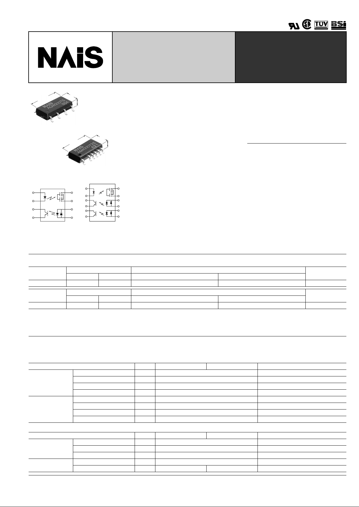
8
1
2
3
4
7
6
5
Relay portion
(1,2,7,8 pins)
Detector portion
(3,4,5,6 pins)
1
12
11
2
4
3
5
6
10
9
8
7
+
–
+
–
+
–
Relay portion
(1,2,11,12 pins)
Detector portion
(3,4,9,10 pins)
(5,6,7,8 pins)
GU (General Use) Type
SOP Series
Multi-function (MOSFET &
optocoupler) T ype
1 optocoupler type
4.4±0.2
.173±.008
2.1±0.2
.083±.008
9.37±0.2
.369±.008
2 optocouplers type
mm inch
4.4±0.2
.173±.008
2.1±0.2
.083±.008
9.37±0.2
.369±.008
FEATURES
1. Multi-function type with MOSFET
and optocoupler
Instead of the conventional arrangement
of a separate PhotoMOS relay and optocoupler, PhotoMOS relay and 2 optocoupler this new multi-function type
encapsulates the PhotoMOS relay and
optocoupler into one SOP package.
2. Ultra-small package size
Integration of the two devices makes a
significant size reduction possible. The
SOP package measures (W) 4.4 × (D)
9.37 × (H) 2.1 mm ((W) .173 × (D) .369 ×
(H) .083 inch).
3. Ideal for PC car d and Fax/Modem applications
The small size provides additional space
for increased functionality, without sacrificing any of the performance of conventional MOSFET relay and optocoupler,
PhotoMOS relay and 2 optocoupler com-
binations. The new device has been specifically designed for the PCMCIA market.
4. Also available in 8-pin SOP package
2 Form A MOSFET relays are also available in a single 8-pin SOP package.
TYPICAL APPLICATIONS
• PCMCIA/JEIDA standard FAX/Modem
card
TYPES
* Indicate the peak AC and DC values.
Notes: (1) Tape package is the standard packing style. Also available in tube. (Part No. suffix "X" or "Z" is not needed when ordering; Tube: 50 pcs.;
Case: 1,000 pcs.)
(2) For space reasons, the package type indicator "X" and "Z" are omitted from the seal.
1 optocoupler
type
Output rating* Part No.
Packing quantity
in tape and reel
Load voltage Load current Picked from the 1/2/3/4-pin side Picked from the 5/6/7/8-pin side
AC/DC type 350 V 120 mA AQW210TSX AQW210TSZ 1,000 pcs.
2 optocouplers
type
Output rating* Part No.
Packing quantity
in tape and reel
Load voltage Load current Picked from the 1/2/3/4/5/6-pin side Picked from the 7/8/9/10/11/12-pin side
AC/DC type 350 V 120 mA AQW210T2SX AQW210T2SZ 1,000 pcs.
RATING
1. Absolute maximum ratings (Ambient temperature: 25 ° C 77 ° F)
Relay portion (1, 2, 7, 8 pins) [AQW210TS], (1,2,11,12 pins) [AQW210T2S]
Detector portion (3, 4, 5, 6 pins) [AQW210TS], (3,4,9,10 and 5,6,7,8 pins) [AQW210T2S]
Item Symbol AQW210TS AQW210T2S Remarks
Input
LED forward current I
F
50 mA
LED reverse voltage V
R
3 V
Peak forward current I
FP
1 A f = 100 Hz, Duty factor = 0.1%
Power dissipation P
in
75 mW
Output
Load voltage V
L
350 V
Continuous load current I
L
0.12 A Peak AC, DC
Peak load current I
peak
0.36 A 100 ms. (1 shot), V
L
= DC
Power dissipation P
out
400 mW
Item Symbol AQW210TS AQW210T2S Remarks
Input
LED forward current I
F
50 mA
Peak forward current I
FP
1 A f = 100 Hz, Duty factor = 0.1%
Power dissipation P
in
75 mW
Output
Output voltage BV
CEC
30 V
Power dissipation P
out
150 mW 100 mW
PhotoMOS
RELAYS
Page 2
AQW210TS, 210T2S
82
Others
2. Electrical characteristics (Ambient temperature: 25 ° C 77 ° F )
Relay portion (1,2,7,8 pins) [AQW210TS] (1,2,11,12 pins) [AQW210T2S]
Note: Recommendable LED forward current I
F
= 5 mA.
Detector portion (3,4,5,6 pins) [AQW210TS] (3,4,9,10 and 5,6,7,8 pins) [AQW210T2S]
Detector portion
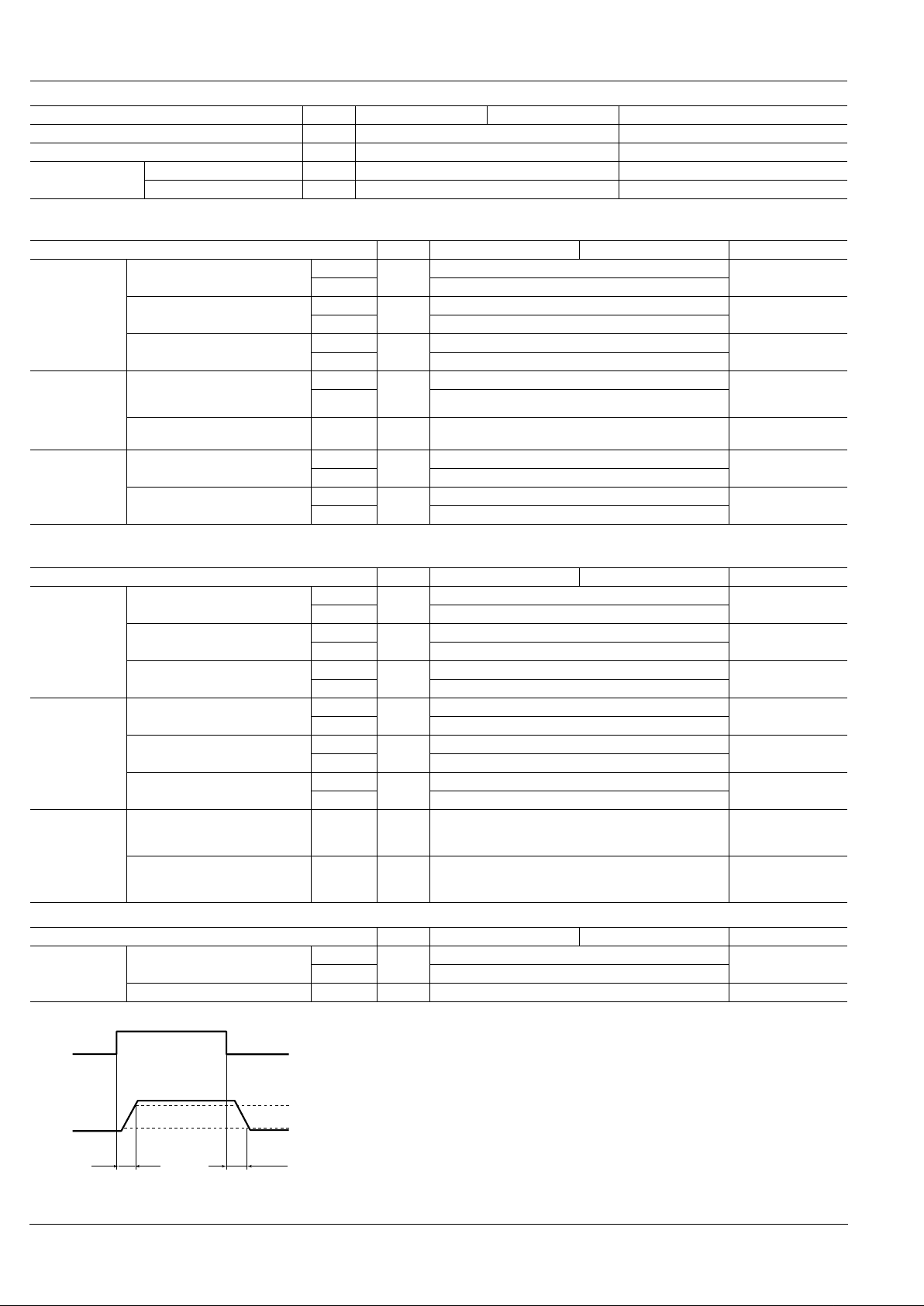
*Turn on/Turn off time For type of connection, see page 33.
Item Symbol AQW210TS AQW210T2S Remarks
Total power dissipation T
P
650 mW
I/O isolation voltage V
iso
1500 V AC
Temperature limits
Operating T
opr
–40 ° C to +85 ° C –40 ° F to +185 ° F Non-condensing at low temperatures
Storage T
stg
–40 ° C to +100 ° C –40 ° F to +212 ° F
Item Symbol AQW210TS AQW210T2S Condition
Input
LED operate current
Typical
I
Fon
0.9 mA
I
L
= Max.
Maximum 3 mA
LED turn off current
Minimum
I
Foff
0.4 mA
I
L
= Max.
Typical 0.8 mA
LED dropout voltage
Typical
V
F
1.14 V (1.25 V at I
F
= 50 mA)
I
F
= 5 mA
Maximum 1.5 V
Output
On resistance
Typical
R
on
16 Ω
I
F
= 5 mA
I
L
= Max.
Within 1 s on time
Maximum 35 Ω
Off state leakage current Maximum I
leak
1 µ A
I
F
= 0
I
L
= Max.
Transfer
characteristics
Turn on time*
Typical
T
on
0.23 ms
I
F
= 5 mA
I
L
= Max.
Maximum 0.5 ms
Turn off time*
Typical
T
off
0.04 ms
I
F
= 5 mA
I
L
= Max.
Maximum 0.2 ms
Item Symbol AQW210TS AQW210T2S Condition
Input
LED operate current
Typical
I
Fon
2 mA
I
C
= 2 mA
V
CE
= 0.5 V
Maximum 6 mA
LED turn off current
Minimum
I
Foff
5 µ A
I
C
= 1 µ A
V
CE
= 5 V
Typical 35 µ A
LED dropout voltage
Typical
V
F
1.14 V (1.25 V at I
F
= 50 mA)
I
F
= 5 mA
Maximum 1.5 V
Output
Saturation voltage
Typical
V
on
0.08 V
I
F
= 15 mA
I
C
= 2 mA
Maximum 0.5 V
Off state leakage current
Typical
I
CEO
0.01 nA
I
F
= 0
V
CE
= 5 V
Maximum 500 nA
Current transfer ratio
Minimum
—
33 %
I
F
= 5 mA
V
CE
= 0.5 V
Typical 100 %
Transfer
characteristics
Turn on time* Typical T
on
0.01 ms
I
F
= 5 mA
V
CE
= 5 V
I
C
= 2 mA
Turn off time* Typical T
off
0.03 ms
I
F
= 5 mA
V
CE
= 5 V
I
C
= 2 mA
Item Symbol AQW210TS AQW210T2S Remarks
Input
I/O capacitance
Typical
C
iso
0.8 pF
f = 1 MHz
V
B
= 0
Maximum 1.5 pF
Intial I/O isolation resistance Minimum R
iso
1,000 M Ω
DC 500 V
Ton
Input
Output 10%
90%
Toff
■
For Dimensions, see Page 28.
■
For Schematic and Wiring Diagrams, see Page 33.
■
For Cautions for Use, see Page 36.
Page 3

AQW210TS, 210T2S
83
REFERENCE DATA
[1] Relay portion (1, 2, 7, 8 pins) [AQW 210TS] (1, 2, 11, 12 pins) [AQW210T2S]
1. Load current vs. ambient temperature characteristics
Allowable ambient temperature: –40 ° C to + 85 ° C
–40 ° F to +185 ° F
2. On resistance vs. ambient temperature characteristics
Measured portion: between terminals 7 and 8 (AQW210TS),
11 and 12 (AQW210T2S); LED current: 5 mA; Load voltage:
Max. (DC); Continuous load current: Max. (DC)
3. Turn on time vs. ambient temperature characteristics
LED current: 5 mA; Load voltage: Max. (DC);
Continuous load current: Max. (DC)
0
20
40
60
80
100
120
–40 –20 0 20 40 60 8085 100
Ambient temperature, °C
Load current, mA
0
50
40
30
20
10
–40 –20 0 20 40 60 8085
Ambient temperature, °C
On resistance, Ω
0
0.2
0.4
0.6
0.8
1.0
–40 –20 0 20 40 60 8085
Ambient temperature, °C
Turn on time, ms
4. Turn off time vs. ambient temperature characteristics
LED current: 5 mA; Load voltage: Max. (DC);
Continuous load current: Max. (DC)
5. LED operate current vs. ambient temperature characteristics
Load voltage: Max. (DC);
Continuous load current: Max. (DC)
6. LED turn off current vs. ambient temperature
characteristics
Load voltage: Max. (DC);
Continuous load current: Max. (DC)
0.4
0.3
0.2
0.1
0
–20–40 0 20 40 60 8085
Ambient temperature, °C
Turn off time, ms
0
1
2
3
4
5
–40 –20 0 20 40 60 8085
Ambient temperature, °C
LED operate current, mA
0
1
2
3
4
5
–40 –20 0 20 40 60 8085
Ambient temperature, °C
LED turn off current, mA
7. LED dropout voltage vs. ambient temperature characteristics
LED current: 5 to 50 mA
8. Voltage vs. current characteristics of output
at MOS portion
Measured portion: between terminals 7 and 8
(AQW210TS), 11 and 12 (AQW210T2S); Ambient
temperature: 25°C 77°F
9. Off state leakage current
Measured portion: between terminals 7 and 8
(AQW210TS), 11 and 12 (AQW210T2S);
Ambient temperature: 25°C 77°F
0
1.0
1.1
1.2
1.3
1.4
1.5
–40 –20 0 20 40 60 8085
50 mA
30 mA
20 mA
5 mA
10 mA
Ambient temperature, °C
LED dropout voltage, V
–5 –4 –3 –2 –1
12345
120
100
80
60
40
20
–20
–40
–60
–80
–100
–120
Voltage, V
Current, mA
0 20406080100
10
–12
10
–9
10
–6
10
–3
Load voltage, V
Off state leakage current, A
10. LED forward current vs. turn on time characteristics
Measured portion: between terminals 7 and 8 (AQW210TS), 11
and 12 (AQW210T2S); Load voltage: Max. (DC); Continuous
load current: Max. (DC); Ambient temperature: 25°C 77°F
11. LED forward current vs. turn off time characteristics
Measured portion: between terminals 7 and 8 (AQW210TS), 11
and 12 (AQW210T2S); Load voltage: Max. (DC); Continuous
load current: Max. (DC); Ambient temperature: 25°C 77°F
12. Applied voltage vs. output capacitance
characteristics
Measured portion: between terminals 7 and 8
(AQW210TS), 11 and 12 (AQW210T2S); Frequency:
1 MHz; Ambient temperature: 25°C 77°F
0 102030405060
0
0.2
0.4
0.6
0.8
1.0
1.2
1.4
LED forward current, mA
Turn on time, ms
0 102030405060
0
0.02
0.04
0.06
0.08
0.10
LED forward current, mA
Turn off time, ms
0
10
20
30
40
50
0 1020304050
Applied voltage, V
Output capacitance, pF
Page 4

AQW210TS, 210T2S
84
[2] Detector portion (3, 4, 5, 6 pins) [AQW 210TS] (3/4/9/10 pins and 5/6/7/8 pins) [AQW210T2S]
1. Output loss vs. ambient temperature characteristics
Allowable temperature range: –40° to 85°C
–40 to 185°F
2. Relativ e output current vs. ambient temperature characteristics
Measured portion: between terminals 3 and 4
(AQW210TS), 3 and 4, 5 and 6 (AQW210T2S)
I
F = 5 mA, VCE = 0.5 V DC
3. LED dropout voltage vs. ambient temperature characteristics
LED current: 5 to 50 mA
–40 –20 0 20 40 60 8085100
0
50
100
150
200
AQW210TS
AQW210T2S
Ambient temperature, °C
Output loss, mW
–40 –20 0 20 40 60 8085100
0
50
100
150
Ambient temperature, °C
Relative output current, %
0
1.0
1.1
1.2
1.3
1.4
1.5
–20–40 0 20 40 60 8085
50 mA
30 mA
20 mA
10 mA
5 mA
Ambient temperature, °C
LED dropout voltage, V
4-1. Collector current vs. voltage between collector and emitter characteristics (IC-VCE)
Measured portion: between terminals 3 and 4
(AQW210TS), 3 and 4, 5 and 6 (AQW210T2S)
Ambient temperature: 25°C 77°F
4-2. Collector current vs. voltage between collector and emitter characteristics (IC-VCE)
Measured portion: between terminals 3 and 4
(AQW210TS), 3 and 4, 5 and 6 (AQW210T2S)
Ambient temperature: 25°C 77°F
5. Off state leakage current
Measured portion: between terminals 3 and 4
(AQW210TS), 3 and 4, 5 and 6 (AQW210T2S)
LED current: 0 mA
Ambient temperature: 25°C 77°F
0
0
20
40
60
80
246810
PC (Max.)
I
F=50 mA
I
F=40 mA
I
F=30 mA
IF=20 mA
I
F=10 mA
I
F=5 mA
Voltage between collector and emitter, V
Collector current, mA
AQW210TS
AQW210T2S
0
0
10
20
30
40
0.1 0.2 0.3 0.4 0.5
IF=50 mA
I
F=40 mA
IF=30 mA
I
F=20 mA
IF=10 mA
IF=5 mA
Voltage between collector and emitter, V
Collector current, mA
0 102030
10
–12
10
–9
10
–6
10
–3
Voltage between collector and emitter, V
Off state leakage current, A
5/7/2001 All Rights Reserved, © Copyright Matsushita Electric Works, Ltd.
Go To Online Catalog
 Loading...