

Datasheet APX9141DEE-TR, APX9141DEE-TB, APX9141DEE-PB, APX9141BEE-PB, APX9141ATEE-TR Datasheet (ANPEC)
...Page 1
APX9141
Hall Effect Sensor IC with Reverse Voltage Protection
Features General Description
••
•
On-chip Reverse Voltage Protection
••
••
•
On-chip Hall Sensor
••
••
•
Low Operating Supply Voltage : 3 V
••
••
•
High Output Sinking Capability up to 400mA
••
••
•
Versatile sensitivity and hysteresis setting
••
••
•
Reliable and Rugged
••
••
• 4 pin TO-92M Package
••
Applications
••
• Brushless DC Fan
••
••
• Revolution Counting
••
••
• Brushless DC Motor
••
••
• Speed Measurement
••
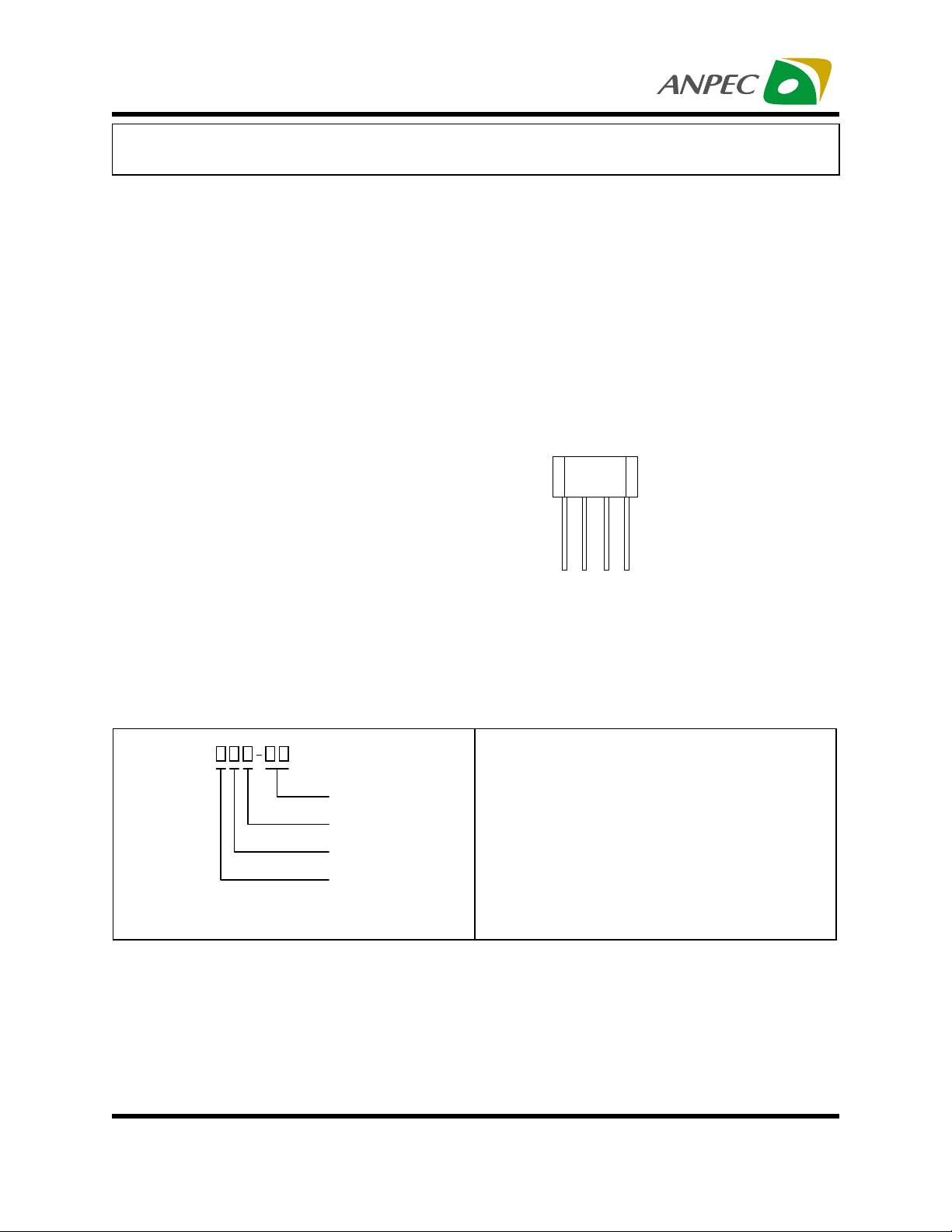
Ordering Information
The APX9141 is an integrated Hall Effect Sensor
IC designed for electric commutation of DC
brushless motor applications. The APX9141 still can
operate at as low as 3 volts. The APX9141 is available in low cost TO -92M4 package with 3 different
magnetic ranks.
Pin Description
APX9141
1
23
4
Front View
1 : V
DD
2 : DO
3 : DOB
4 : GND
Magnetic Rank
APX9141
Handling Code
Temp. Range
Package Code
Magnetic Rank
ANPEC reserves the right to make changes to improve reliability or manufacturability without notice, and advise
customers to obtain the latest version of relevant information to verify before placing orders.
Copyright ANPEC Electronics Corp.
Rev. A.6 - Jan., 2003
AT : | Bop , Brp | < 50 Gauss
A : | Bop , Brp | < 70 Gauss
B : | Bop , Brp | < 100 Gauss
D : | Bop , Brp | < 150 Gauss
Package Code
E : TO - 92M4
Temp. Range
E : -20 to 85 C
Handling Code
PB : Plastic Bag TB : Tape & Box
TR : Tape & Reel
°
www.anpec.com.tw1
Page 2
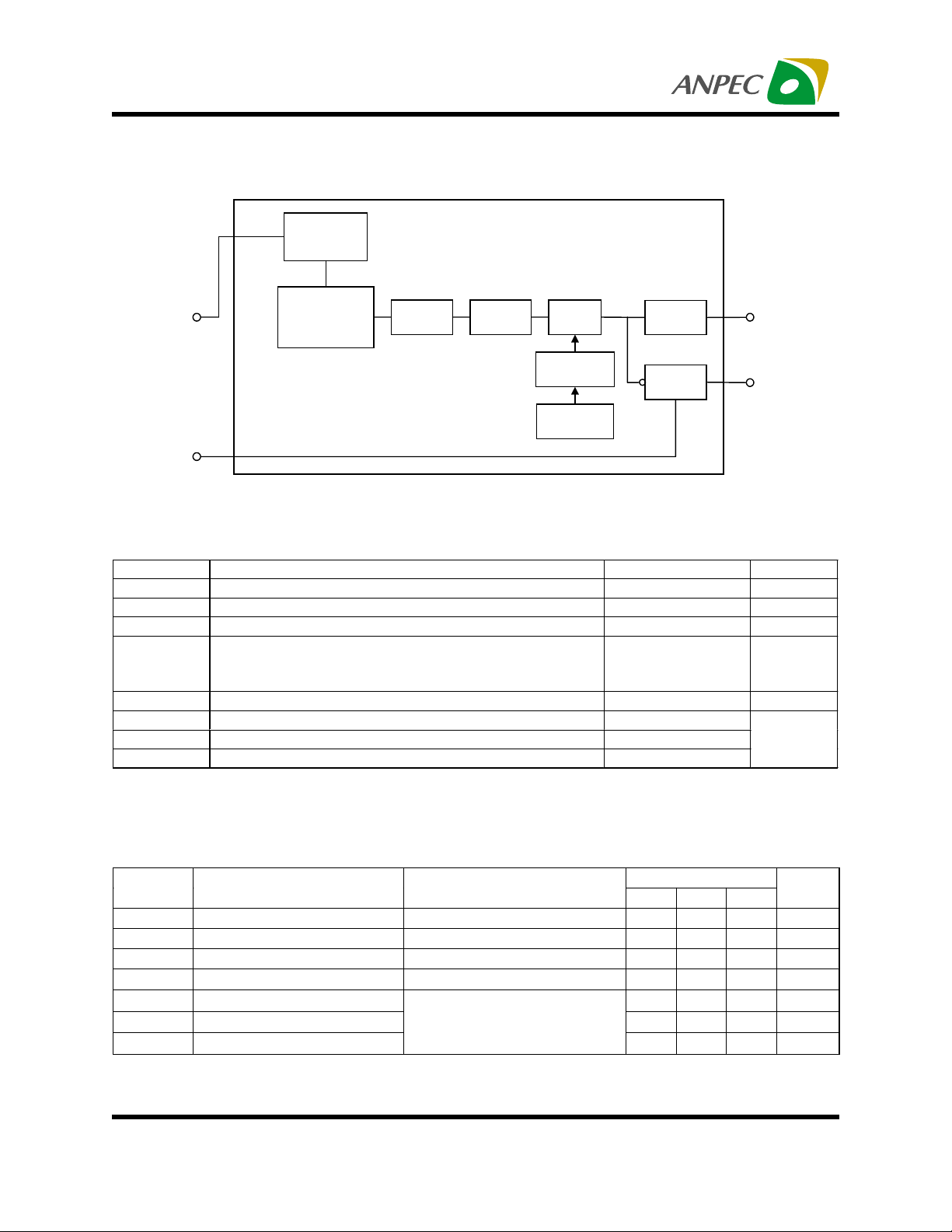
APX9141
Block Diagram
Reverse
Voltage
Protection
APX9141
Temperature
V
DD
Gnd
Compensated
Voltage
Regulator
Absolute Maximum Ratings T
Hall
Element
Current
Amplif ier
= 25°C unless otherwise noted
A
Latch
Circuit
Hysteresis
Control
Se n s it iv ity
Control
Output
Buffe r 1
Output
Buffe r 2
Symbol Parameter Rating Unit
T
T
V
V
I
I
P
T
DD
BD
DD
OUT
D
A
STG
SOL
Supply Voltage 20 V
Output Breakdown Voltage 55 V
Supply Current 25 mA
Output Current – Continuous
Hold Current
Peak (Start Up)
400
600
800
Maxim um P ow er Dissipation 500 mW
Operating Ambient Tem perature -20 to 85
Storage Temperature Range -65 to 150
Soldering Temperature (10 Sec.) 260
DOB
DO
mA
C
°
Electrical Characteristics T
V
I
V
I
Leak
t
t
∆
Supply Voltage Operating 3 20 V
DD
Output Saturation Voltage VDD=14V, I
SAT
Supply Current VDD=20V, Output Open 20 25 mA
DD
a
Output Leakage Current V
b
Output Rise Time 0.8 5
r
b
Output Fall Time 0.1 1
f
b
Switch Time Different
t
= 25°C, VDD=20V unless otherwise noted
A
=20V, VDD=20V, B<Brp <0.1 10
OUT
V
=14V, RL=820
DD
C
=20pF
L
Note a : No leakage current spike when IC start-up
b : use Figure 1
Copyright ANPEC Electronics Corp.
Rev. A.6 - Jan., 2003
APX9141Symbol Parameter Test Condition
Min. Typ. Max.
=400mA, B>Bop 250 500 mV
OUT
Ω
3.5 7
www.anpec.com.tw2
Unit
A
µ
s
µ
s
µ
s
µ
Page 3
APX9141
Magnetic Characteristics T
Rank Maximum Operate
Point Bop
= 25°C, VDD=14V unless otherwise noted
A
Maximum Release
Point Brp
Unit
AT +50 -50
A+70 -70
B +100 -100
Gauss
D +150 -150
Note : For 5cm and below DC fan application, grade A/AT device is recommended to avoid magnetic
sensitivity problem. For above 5cm DC fan application, grade B device is acceptable for most cases.
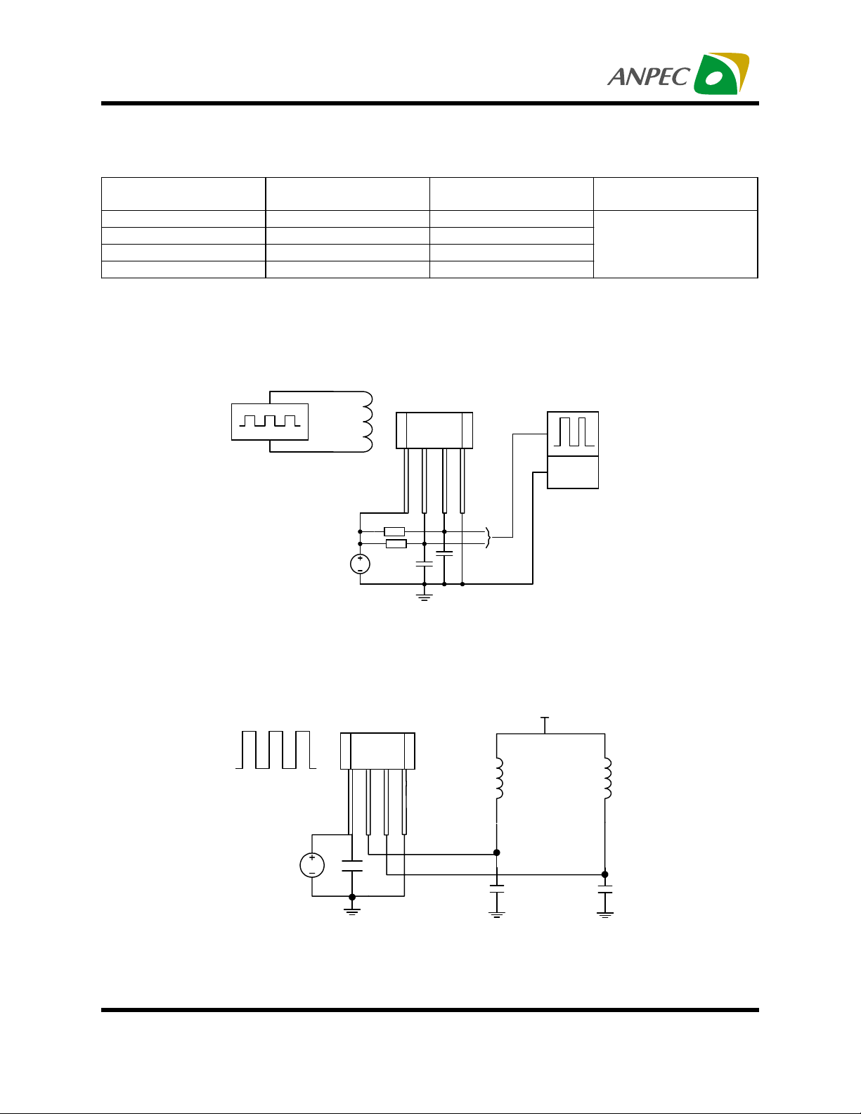
Test Information
APX9141
2314
Signal Generator
Scope
R
L2
R
V
DD
L1
C
L2
C
L1
Figure 1 : Switching Circuit for Output Rise Time and Fall Time Measurement
Application Circuit
APX9141
+B
-B
231
4
V
DD
C1
Figure 2 Typical DC brushless fan application circuit
V
DD
L1 L2
C3C2
Copyright ANPEC Electronics Corp.
Rev. A.6 - Jan., 2003
www.anpec.com.tw3
Page 4

APX9141
Typical Characteristics
Supply Current vs. Supply Voltage
25
TA=25°C
20
15
10
5
0
Supply Current (mA)
-5
-10
-30 -20 -10 0 10 20 30 40 50
Supply Voltage (V)
Output Saturation Voltage vs. Output Current
250
200
150
100
50
Output Saturation Voltage (mV)
0
0 100 200 300 400 500
Output Current (mA)
Output Low Voltage vs Ambient Temperature
300
IOUT=400mA
VDD=14V
275
250
225
200
Output Low Voltage (mV)
175
150
-20 0 20 40 60 80 100
Temperature (°C)
Supply Current vs Temperature
25
VCC=20V
20
15
10
VCC=3V
VCC=14V
Supply Current (mA)
5
0
-20 0 20 40 60 80 100
Temperature (°C)
Copyright ANPEC Electronics Corp.
Rev. A.6 - Jan., 2003
www.anpec.com.tw4
Page 5

APX9141
Typical Characteristics (Cont.)
Magnetic Switch Points vs Supply Voltage
100
80
60
40
20
0
-20
-40
-60
Magnetic Switch Points (G)
-80
-100
0 5 10 15 20
Bop
Brp
Supply Voltage (V)
IOUT=400mA
TA=25°C
Magnetic Switch Points vs Temperature
150
IOUT=400mA
DD=14V
100
50
0
-50
-100
Magnetic Switch Points (G)
-150
-20 0 20 40 60 80 100
Bop
Brp
Temperature (°C)
V
Power Dissipation vs. Ambient Temperature
600
500
400
300
200
100
Power Dissipation (mW)
0
0 25 50 75 100 125 150
Ambient Temperature (°C)
Output Breakdown Voltage vs. Current
1
0.9
0.8
0.7
0.6
0.5
0.4
0.3
Output Current (uA)
Output Breakdown Voltage
0.2
0.1
0
0 102030405060
Output Voltage (V)
Copyright ANPEC Electronics Corp.
Rev. A.6 - Jan., 2003
www.anpec.com.tw5
Page 6

APX9141
Package Information
TO-92M4
M a rk ing S u rfac e
S
E
JD
Sensitive Area (0.286 0.286m m 2)
P o s ition o f H all S en s o r
reference to the top-left of package
x= 0.85 0.1mm
y= 1.95 0.1mm
1.10mm
±
±
IC c h ip
A
1.95mm
C
L
L1
b1
e1
e
×
Min. Max. Min. Max.
A 3.60 3.70 0.141 0.145
b1 0.35 0.41 0.014 0.016
C 0.351 0.411 0.014 0.016
D 5.17 5.27 0.203 0.207
e 3.78 3.84 0.148 0.150
e1 1.24 1.30 0.049 0.051
E 1.50 1.60 0.059 0.063
J 4.04 4.34 0.158 0.170
L 14.0 15.0 0.549 0.588
L1 1.342 1.542 0.053 0.060
S 0.45 0.55 0.018 0.022
Copyright ANPEC Electronics Corp.
Rev. A.6 - Jan., 2003
Millimeters InchesDim
www.anpec.com.tw6
Page 7

APX9141
Customer Service
Anpec Electronics Corp.
Head Office :
5F, No. 2 Li-Hsin Road, SBIP,
Hsin-Chu, Taiwan, R.O.C.
Tel : 886-3-5642000
Fax : 886-3-5642050
Taipei Branch :
7F, No. 137, Lane 235, Pac Chiao Rd.,
Hsin Tien City, Taipei Hsien, Taiwan, R. O. C.
Tel : 886-2-89191368
Fax : 886-2-89191369
Copyright ANPEC Electronics Corp.
Rev. A.6 - Jan., 2003
www.anpec.com.tw7
 Loading...