

Page 1
查询APX9132ATI-TRL供应商
APX9132
Hall Effect Micro Switch IC
Features General Description
• Micro Power Ope ration for Battery Applications
• Chopper Stabilized Amplifier
• Independent of North or South Pole Magnet,
Ea sy for Manufacture
• Small Size Pa ckage
• Lead Free Available (RoHS Compliant)
Ap plic ations
• Micro Switch
• Ha ndheld Wireless Application Wake Up Switch
• Cla mp Shell Type Application Switch
• Magnet Switch in Low Duty Cycle Applications
The APX9132 integrated circ uit is an ultra-sensit ive,
pole independent Hall-effect switch with a latched
di gital output . A 2.5 volt to 3.5 volt operation and a
uniq ue clocking scheme reduce the average operating
power requirements, Either a north or sout h pole of
sufficient flux will turn the output on; in the absence of
a magnetic field, the out put is off. The polarity
i ndependence a nd minimal power requirement allow
t his devic e t o be easily repla ced reed switc h for
s uperior for signal condit ioning. Advanced CMOS
proces sing is used to take advantage of l ow-voltage
a nd low-pow er requirements, SOT-23 package provided
a optimized pa ckage for most applications.
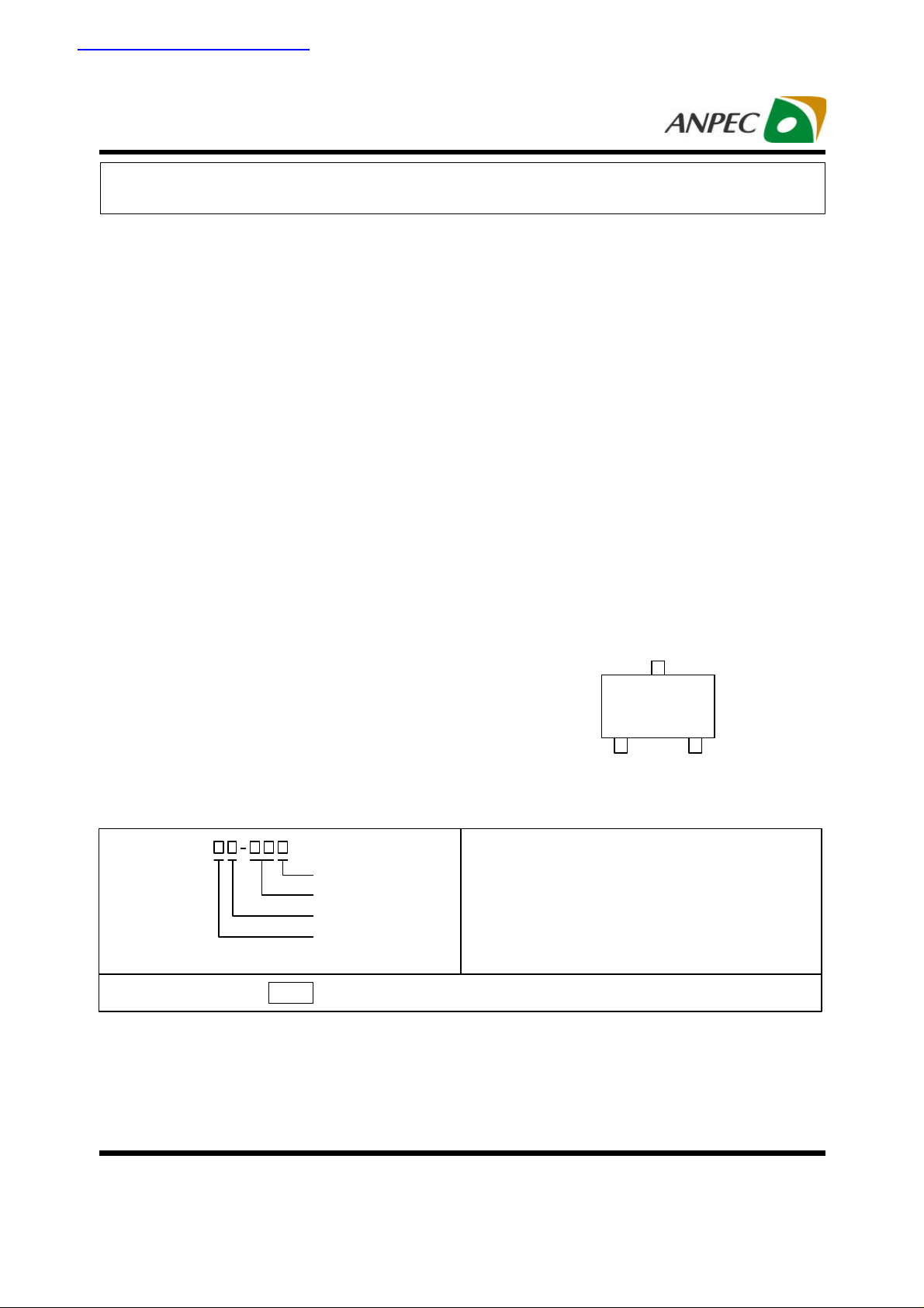
Pin Description
GND
APX9132
VDD
VOUT
SOT-23
Ordering Information
APX9132
Lead Free Code
Handling Code
Temp. Range
Package Code
APX9132 A/AT:
No tes : ANPEC lead-free p roducts contain molding compounds/die attach materials and 100% m atte in plate
te rminatio n finish ; which are full y compliant with Ro HS and compatibl e with both SnPb an d lead-free soldiering
op erations. AN PEC lead-free products meet or exceed the lead -free req uireme nts of IPC/JEDEC J STD-020C
fo r MSL classification at lead-fre e peak reflo w temp erature.
ANPEC reserves the right to make changes to improve reliability or manufacturability without notice, and advise
customers to obtain the latest version of relevant information to verify before placing orders.
C opyright ANPEC Electronics C orp.
Rev. A.1 - Nov., 2005
X32X
Package Code
A : SOT-23 AT : SOT-23 Thin
Temp. Range
I : -40 to 85 C
Handling Code
TR : Tape & Reel
Lead Free Code
L : Lead Free Device Blank : Original Device
X: Date Code
°
www.anpec.com.tw1
Page 2
APX9132
When a magnetic field enters the hall element and exceeds the
) the output turns on (output is
(or
Function Pin Descriptions
No Name Function
1 VDD Power Input
2 V
OUT
operate point B
low). When the magnetic field is below the release point BRPS
above B
RPN
3 GND Ground Connection
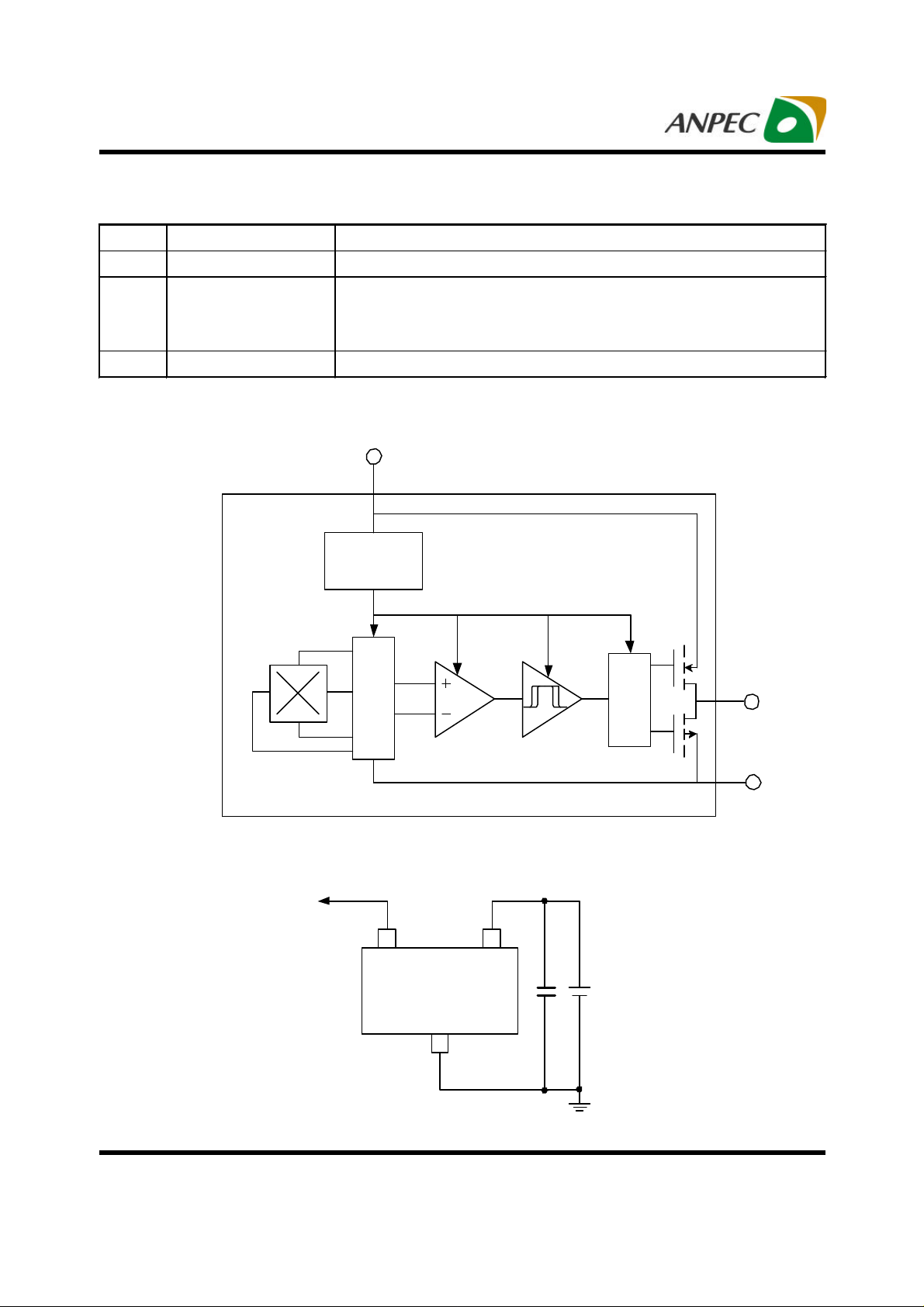
Block Diagram
Hall Plane
VDD
Awake & Sleep
Timing Logic
Cancellation
Dynamic Offset
OPS
(or less than B
OPN
), the output turns off (output is high).
Latch
Circuit
Chopper
Amplifier
Hysteresis
Control
VOUT
GND
Typical Applications
V
OUT
APX9132
GND
SOT-23 (Top View)
C opyright ANPEC Electronics C orp.
Rev. A.1 - Nov., 2005
V
DD
0.1uF
+
2.5V-3.5V
-
www.anpec.com.tw2
Page 3
APX9132
Absolute Maximum Ratings T
= 25°C unless otherwise noted
A
Symbol Parameter Rating Unit
VDD Supply Voltage 5 V
V
Output Voltage 5 V
OUT
I
Output Current
OUT
±
1
TJ Junction Temperature Range 150
T
Storage Temperature Range -65 to +150
STG
Electrical Characteristics T
Symbol
VDD Supply Voltage Range Operating 2.5 3.5 V
IDD Supply Current
I
Output Leakage Current V
OFF
VOH Output High Voltage I
VOL Output Low Voltage I
t
Wake up Time
awake
t
Period
period
d.c. Duty Cycle
fc Chopping Frequency
Characteristic Test Condition
Average 5 10
Awake 1.2 2 mA
Sleep 2 8
SINK
SINK
= 25°C, VDD=3V unless otherwise noted
A
APX9132
Min. Typ. Max.
=3.5V, B
OUT
=-1mA
RPN
<B<B
1.0
RPS
VDD
-0.4
V
=1mA 20 40 mV
180
60 mS
0.3
11 KHz
mA
°
C
Unit
µ
A
µA
µ
A
µ
s
%
Magnetic Characteristics T
= 25°C, VDD=3V unless otherwise noted
A
APX9132
Symbol Characteristic Test Condition
Unit
Min. Typ. Max.
B
OPS
B
OPN
B
RPS
B
RPN
B
Operate Points
Release Points
Hysteresis
hys
30 45 G
-45 -30 G
10 20 G
-20 -10 G
10 G
C opyright ANPEC Electronics C orp.
Rev. A.1 - Nov., 2005
www.anpec.com.tw3
Page 4
APX9132
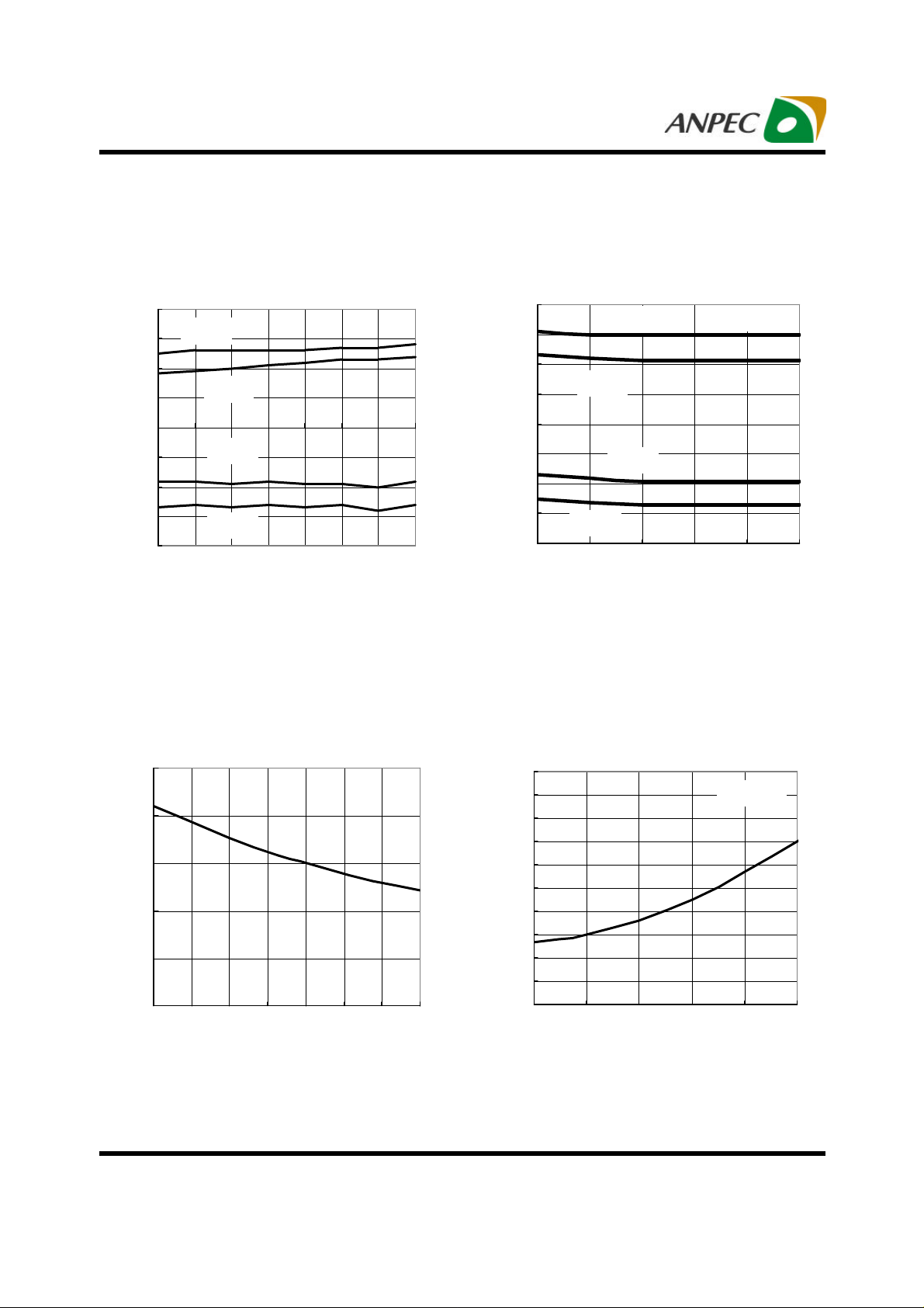
Typical Characteristics
Switching Points vs. Ambient Temperature
40
30
20
10
0
-10
-20
Switching Points (G)
-30
-40
BOPS
BRPS
BRPN
BOPN
-40 -20 0 20 40 60 80 100
Ambient Temperature (°C)
Switching Points vs. Supply Voltage
40
30
20
10
0
-10
-20
Switching Points (G)
-30
-40
2.5 3 3.5 4 4.5 5
BOPS
BRPS
BRPN
BOPN
Supply Voltage (V)
TA=25°C
Average Supply Current vs. Ambient Temperature
10
8
6
4
2
Average Supply Current (uA)
0
-40 -20 0 20 40 60 80 100
Ambient Temperature (°C)
C opyright ANPEC Electronics C orp.
Rev. A.1 - Nov., 2005
Average Supply Current vs.Supply Voltage
20
18
16
14
12
10
8
6
4
2
Average Supply Current (uA)
0
2.5 3 3.5 4 4.5 5
TA=25°C
Supply Voltage (V)
www.anpec.com.tw4
Page 5

APX9132
Vout (0.5V/div)
Vcc=5V
Vcc=4V
Vcc=3V
Typical Characteristics
Output Source Current vs. Output Voltage
5
4
3
2
1
Output Source Current (mA)
0
0 0.2 0.4 0.6 0.8 1
Output Voltage (V)
Output Sink Current vs. Output Voltage
10
9
8
7
6
5
4
3
2
Output Sink Current (mA)
1
0
0
0 0.2 0.4 0.6 0.8 1
Vcc=4V
Vcc=5V
Vcc=3V
Output Voltage (V)
Output Switch Waveform
Vcc=3V
CL=12pF
Vout (0.5V/div)
Output Sink Voltage (0.5V/div)
Time (50us/div)
C opyright ANPEC Electronics C orp.
Rev. A.1 - Nov., 2005
Output Switch Waveform
Vcc=3V
CL=12pF
Output Sink Voltage (0.5V/div)
Time (50us/div)
www.anpec.com.tw5
Page 6

APX9132
Function Description
Operation
The output of APX9132 switches low (turns on) when
in pres ence of strong flux density facing the marked
side of package exceeds the operate point B
less than B
). After turn-on, the output is capable of
OPN
OPS
(or is
sinking up to 1mA and the output voltage is low (turns
on). In absence of flux density below the release point
B
(or i ncreased above B
RPS
), the APX9132 output
RPN
switc hes high (turns off). After turn-off, the output is
capable of sourcing up to 1mA and the o utput voltage
is high (turns off). The difference in the magnetic operated and released point is the hysteresis (B
) of the
hys
device. This b uilt-in hysteresis allows clean switching
of the output even in the pres ence of external mecha nical bouncing vibration a nd electrical noise.
5V
MAX
B
OPN
OUTPUT OFF
B
OPS
Pole-independent
The pol e-independent sensing technique allows for
operation with either a north or south pole magnet
orientation, enhancing t he ma nufacturabilit y of t he
device. The stat e-of-the-art technology provides the
sa me output polarity for either pole in presence.
Awake & Sleep
Internal awake & sleep timing block circuit activates
the sensor for 180 us and deac tivates it for the remainder of the period (60 ms). A short “awake” time
all ows for stabilizat ion prior to the sensor sampling
and data latching on the falling edge of the timing pulse.
While in sleep cycle the output is latched in its previous state.
Chopper Stabilized Technique
The chopper stabiliz ed technique cancels the mismatching of the hall element, the amplifier offset voltage and temperature sensitive drift by the dynamic
offset cancellation and switched capacitor technique.
This technique produces devices have an extremely
st able Hall output voltage, therefore the magnetic
switch points are stable.
OUTPUT VOLTAGE
B
RPN
0
MAGNETIC FLUX
B
RPS OUTPUT ON
0 +B-B
Application Information
It is strongly recommended that an ex ternal bypass
capacit or be connected (in close to the Hall sensor)
bet ween the s upply and ground of the devic e to reduce both external noise and noise generated by the
chop per-stabilization technique. This is especially true
due to the relatively high impedance of battery supplies.
C opyright ANPEC Electronics C orp.
Rev. A.1 - Nov., 2005
www.anpec.com.tw6
Page 7

APX9132
Pac kage Information
SOT-23
D
B
3
E H
2
A
L
Dim
1
e
A1
Millimeters Inches
Min. Max. Min. Max.
A 1.00 1.30 0.039 0.051
A1 0.00 0.10 0.000 0.004
B 0.35 0.51 0.014 0.020
C 0.10 0.25 0.004 0.010
D 2.70 3.10 0.106 0.122
E 1.40 1.80 0.055 0.071
e 1.90/2.1 BSC. 0.075/0.083 BSC.
H 2.40 3.00 0.094 0.118
L 0.37 0.015
C
C opyright ANPEC Electronics C orp.
Rev. A.1 - Nov., 2005
www.anpec.com.tw7
Page 8

APX9132
Pac kage Information
SOT-23 Thin
D
b
3
E1 E
1
2
e
e1
L1
R
A
A2
θ
L
c
A1
Dim
A 0.75 0.80 0.028 0.031
A1 0.025 0.05 0.001 0.002
A2 0.75 0.775 0.029 0.030
b 0.35 0.51 0.014 0.020
c 0.10 0.20 0.004 0.008
D 2.80 3.00 0.109 0.117
E 2.60 3.00 0.101 0.117
E1 1.50 1.70 0.059 0.066
e 0.95 BSC 0.037 BSC
e1 1.90 BSC 0.074 BSC
L 0.37 0.60 0.014 0.023
L1 0.60 REF 0.0234 REF
R 0.10 - 0.004 -
θ 0° 8° 0° 8°
Min. Max. Min. Max.
Millimeters Inches
C opyright ANPEC Electronics C orp.
Rev. A.1 - Nov., 2005
www.anpec.com.tw8
Page 9

APX9132
Physic al Specifications
Terminal Material Solder-Plated Copper (Solder Material : 90/10 or 63/37 SnPb), 100%Sn
Lead Solderability Meets EIA Specification RSI86-91, ANSI/J-STD-002 Category 3.
Packaging 3000 devices per reel
Reflow Condition (IR/Convection or VPR Reflow)
T
P
Ramp-up
T
L
Tsmax
Tsmin
Temperature
ts
Preheat
25
°
t 25 C to Peak
Classificatin Reflow Profiles
tp
Ramp-down
Time
Critical Zone
TL to T
P
t
L
Profile Feature Sn-Pb Eutectic Assembly Pb-Free Assembly
Average ramp -up rate
(TL to TP)
Preheat
-
Temperature Min (Tsmin)
-
Temperature Max (Tsmax)
-
Time (min to max) (ts)
Time maintained above:
-
Temperature (TL)
-
Time (tL)
Peak/Classificatioon Temperature (Tp)
Time within 5°C of actual
Peak Temperature (tp)
Ramp-down Rate
Time 25°C to Peak Temperature
3°C/second max. 3°C/second max.
100°C
150°C
60-120 seconds
183°C
60-150 seconds
150°C
200°C
60-180 seconds
217°C
60-150 seconds
See table 1 See table 2
10-30 seconds 20-40 seconds
6°C/second max. 6°C/second max.
6 minutes max. 8 minutes max.
Notes: All temperatures refer to topside of the package .Measured on the body surface.
C opyright ANPEC Electronics C orp.
Rev. A.1 - Nov., 2005
www.anpec.com.tw9
Page 10

APX9132
Classificatin Reflow Profiles(Cont.)
Table 1. SnPb Entectic Process – Package Peak Reflow Temperatures
Package Thickness Volume mm
<350
<2.5 mm
≥
2.5 mm 225 +0/-5°C 225 +0/-5°C
240 +0/-5°C 225 +0/-5°C
3
Volume mm
≥
350
3
Table 2. Pb-free Process – Package Classification Reflow Temperatures
Package Thickness Volume mm3
<350
<1.6 mm
1.6 mm – 2.5 mm
≥
2.5 mm 250 +0°C* 245 +0°C* 245 +0°C*
260 +0°C* 260 +0°C* 260 +0°C*
260 +0°C* 250 +0°C* 245 +0°C*
*Tolerance: The device manufacturer/supplier
shall
Volume mm3
350 -2000
Volume mm3
>2000
assure process compatibility up to and
including the stated classification temperature (this means Peak reflow temperature +0°C.
For example 260°C+0°C) at the rated MSL level.
Reliability test program
Test item Method Description
SOLDERABILITY MIL-STD-883D-2003
HOLT MIL-STD-883D-1005.7 1000 Hrs Bias @ 125 °C
PCT JESD-22-B, A102
TST MIL-STD-883D-1011.9
ESD MIL-STD-883D-3015.7 VHBM > 2KV, VMM > 200V
Latch-Up JESD 78 10ms , Itr > 100mA
245°C , 5 SEC
168 Hrs, 100 % RH , 121°C
-65°C ~ 150°C, 200 Cycles
Car rier Tape & Reel Dimensions
E
F
W
C opyright ANPEC Electronics C orp.
Rev. A.1 - Nov., 2005
Po
P
Ao
t
D
P1
Bo
Ko
D1
www.anpec.com.tw10
Page 11

APX9132
Carrier Tape & Reel Dimensions(Cont.)
J
C
A
T2
B
T1
Application
SOT-23
Application
SOT-23 Thin
A B C J T1 T2 W P E
178±1 60 ± 1.0 12.0 2.5 ± 0.15 9.0 ± 0.5
F D D1 Po P1 Ao Bo Ko t
φ
3.5 ± 0.05 1.5 +0.1
A B C J T1 T2 W P E
178±1 60 ± 1.0 12.0 2.5 ± 0.15 9.0 ± 0.5
F D D1 Po P1 Ao Bo Ko t
φ
3.5 ± 0.05
1.55+
0.05
0.1MIN
φ
1.1±0.1 4.0±0.1 2.0 ± 0.05 3.3±0.1 3.2±0.1 1.1±0.1 0.25±0.05
4.0 2.0 ± 0.05
1.4
3.1 3.0 1.3 0.2±0.03
1.4
8.0+ 0.3
- 0.3
8.0+ 0. 2
4.0 1.75
4.0±0.1 1.75±0.1
Cov er Tape Dimensions
Application Carrier Width Cover Tape Width Devices Per Reel
SOT- 23 8 5.3 3000
SOT- 23 Thin 8 5.3 3000
(mm)
Cus tomer Service
Anpec Electronics Corp.
Head Office :
No.6, Dusing 1st Road, SBIP,
Hsin-Chu, Taiwan, R.O.C.
Tel : 886-3-5642000
Fax : 886-3-5642050
(mm)
Taipei Branch :
7F, No. 137, Lane 235, Pac Chiao Rd.,
Hsin Tien City, Taipei Hsien, Taiwa n, R. O. C.
Tel : 886-2-89191368
Fax : 886-2-89191369
C opyright ANPEC Electronics C orp.
Rev. A.1 - Nov., 2005
www.anpec.com.tw11
 Loading...