

Datasheet APX9031CEE-TR, APX9031CEE-PB, APX9031CDE-TR, APX9031CDE-PB, APX9031BEE-TR Datasheet (ANPEC)
...Page 1
APX9031
Hall Effect Sensor IC
Features General Description
••
•
On-chip Hall Sensor
••
••
•
Low Operating Supply Voltage : 3 V with Re-
••
verse Voltage Protection
••
•
Versatile sensitivity and hysteresis setting
••
••
•
Reliable and Rugged
••
••
•
TO-92M3 and SOT-89 packages
••
Applications
••
• Brushless DC Motor
••
••
• Brushless DC Fan
••
••
• Speed Measurement
••
••
• Revolution Counting
••
Ordering Information
The APX9031 is an integrated Hall Effect Sensor IC
designed for electric commutation of DC brushless
motor applications. Even with a reverse voltage protection diode, the APX9031 still can operate at as
low as 3 volts. The APX9031 is available in low cost
TO-92M3 and SOT-89 packages with 3 different
magnetic ranks.
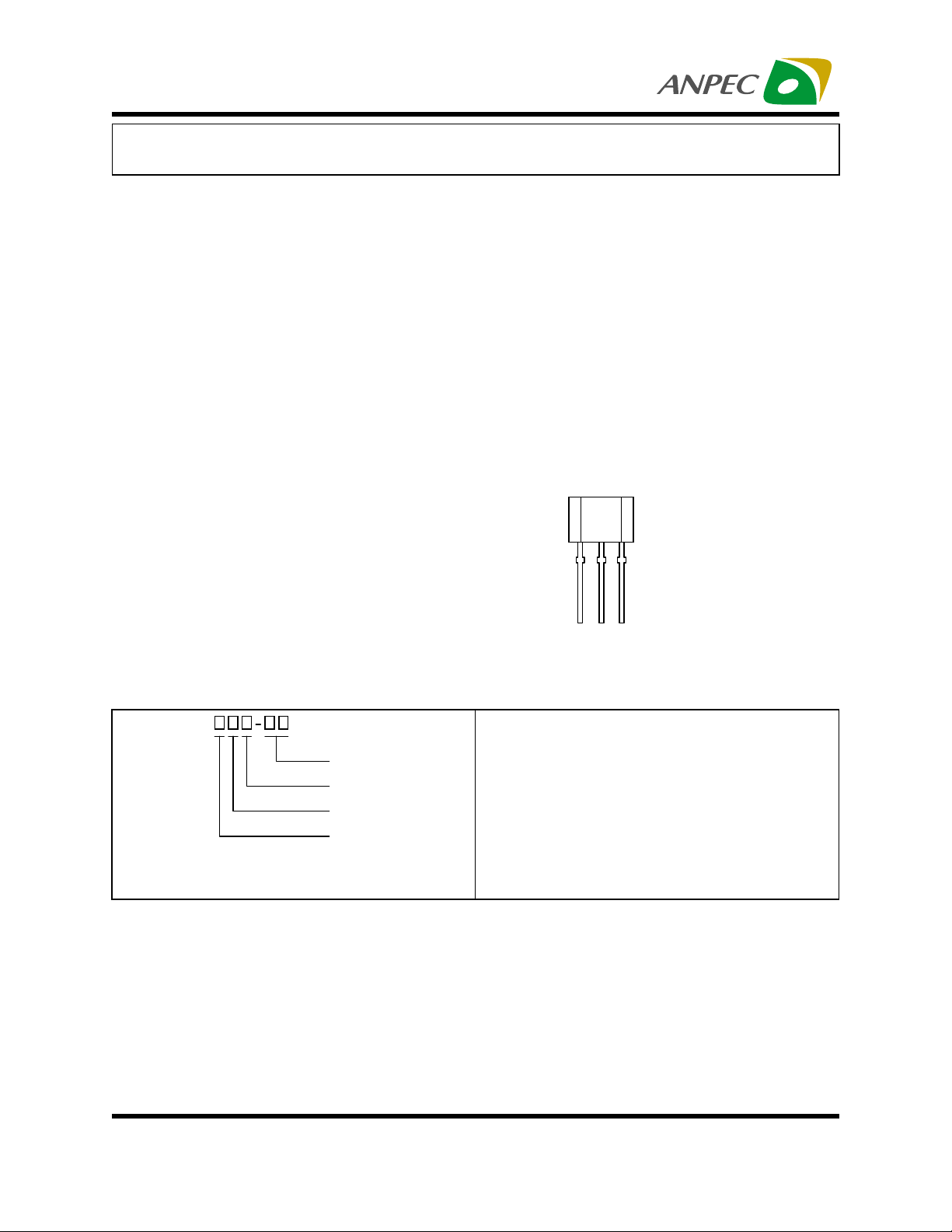
Pin Description
Front View
1 : V
DD
2 : GND
3 : OUTPUT
23
1
APX9031
Handling Code
Temp. Range
Package Code
Magnetic Rank
ANPEC reserves the right to make changes to improve reliability or manufacturability without notice, and advise
customers to obtain the latest version of relevant information to verify before placing orders.
Copyright ANPEC Electronics Corp.
Rev. A.3 - Apr., 2001
Magnetic Rank
A : l Bop , Brp l < 70Gauss
B : l Bop , Brp l < 100 Gauss
C : l Bop , Brp l < 150 Gauss
Package Code
E : TO - 92M
D : SOT - 89
Temp. Range
E: - 20 to 85 C
Handling Code
PB : Plastic Bag
TR : Tape & Reel
°
www.anpec.com.tw1
Page 2
APX9031
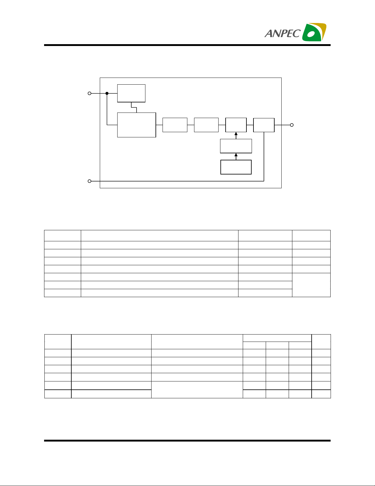
Block Diagram
V
DD
Reverse
Voltage
Protection
APX9031
Temperature
Compensated
Voltage
Regulator
Hall
Element
Current
Amplifier
Latch
Circuit
Hysteresis
Control
Sensitivity
Control
Output
Buffer
Output
Gnd
Absolute Maximum Ratings T
= 25°C unless otherwise noted
A
Symbol Parameter Rating Unit
V
DD
I
DD
I
O
P
D
T
A
T
STG
T
S
Supply Voltage 20 V
Supply Current 8 mA
Output Current 20 mA
Maximum Power Dissipation 400 mW
Operating Ambient Temperature -20 to 85
Storage Temperature Range -55 to 150
Soldering Temperature (10 seconds) 260
C
°
Electical Characteristics
V
V
I
Notes a : use Figure 1
Copyright ANPEC Electronics Corp.
Rev. A.3 - Apr., 2001
Supply Voltage Operating 3 20 V
DD
Output Saturation Voltage I
SAT
I
Supply Current VDD=20V, B<Brp 3.5 6 mA
DD
Output Leakage Current V
Leak
a
t
Output Rise Time 0.6
r
a
t
Output Fall Time
f
OUT
V
TA = 25°C, VDD=12V unless otherwise noted
APX9031Symbol Parameter Test Condition
Min. Typ. Max.
=20mA, B>Bop 0.2 V
=20V, B<Brp 0.5 2
OUT
=12V, RL=820
DD
CL=20pF
Ω,
0.3
www.anpec.com.tw2
Unit
A
µ
s
µ
s
µ
Page 3
APX9031
Magnetic Characteristics T
Rank
Maximum Operate Point
Bop
= 25°C, VDD=12V unless otherwise noted
A
Maximum Release Point
Brp
Unit
A+70 -70
B +100 -100
Gauss
C +150 -150
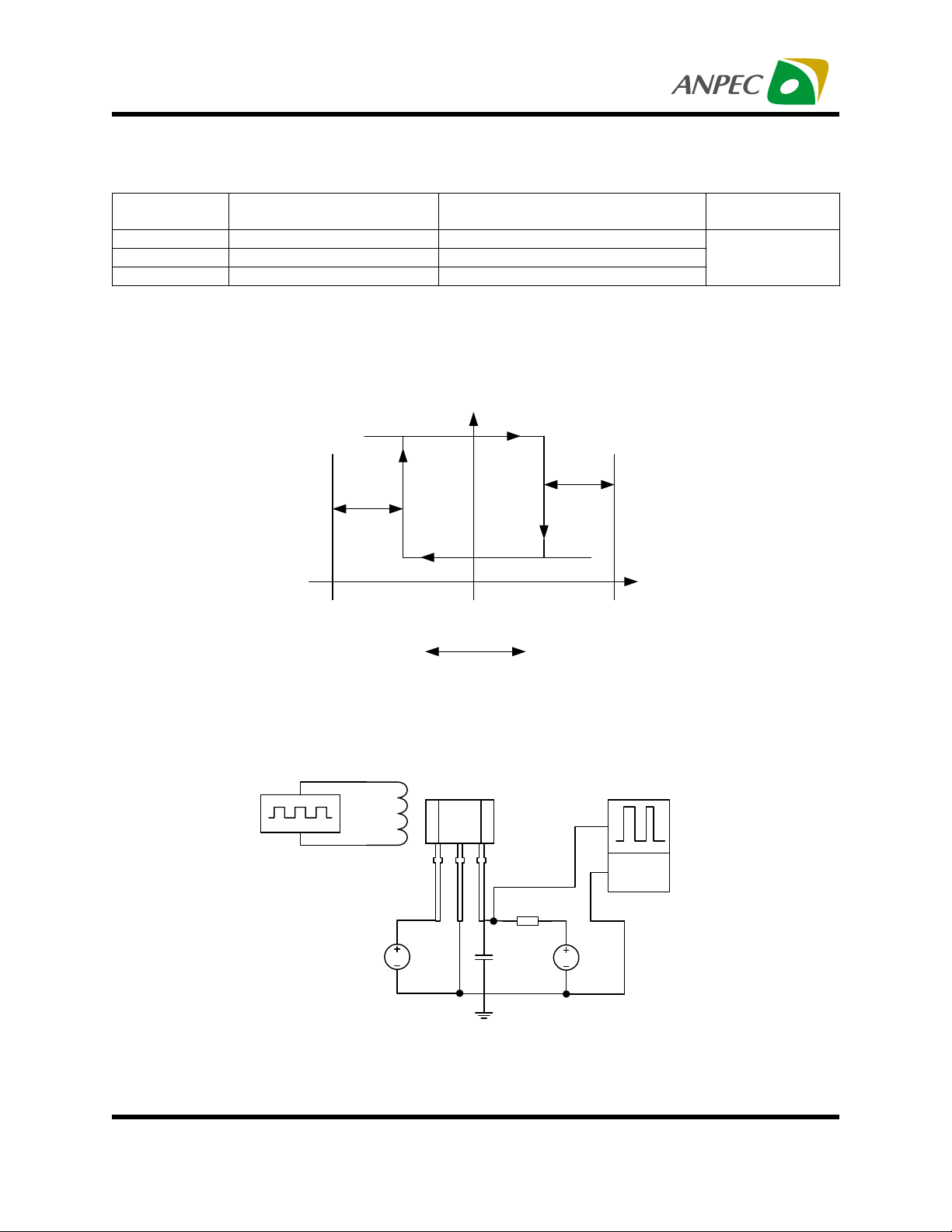
Definition of Magnetic Switching Points and Hysteresis
Output Voltage
Brp min. 0
B
HYS
Bop max.
Test Information
APX9031
23
Signal Generator
Figure 1 : Switching Circuit for Output Rise Time and Fall Time Measurement
1
R
L
V
DD
C
L
Scope
V
DD
Copyright ANPEC Electronics Corp.
Rev. A.3 - Apr., 2001
www.anpec.com.tw3
Page 4

APX9031
Application Circuit
+B
APX9031
V
DD
-B
231
V
DD
Figure 2 Typical DC brushless fan application circuit
Typical Characteristics
Supply Current Vs Supply Voltage
10
TA= 25°C
5
R1
L1 L2
Q1 Q2
Output Low Voltage Vs Supply Voltage
200
TA= 25°C
175
R2
C1 C2
0
-5
Supply Current - mA
-10
-30 -20 -10 0 10 20 30
Supply Voltage - V
Copyright ANPEC Electronics Corp.
Rev. A.3 - Apr., 2001
150
125
Output Low Voltage - mV
100
0 5 10 15 20
Supply Voltage - V
www.anpec.com.tw4
Page 5

APX9031
Typical Characteristics Cont.
Output Low Voltage vs Ambient Temperature
225
I
=20mA
OUT
V
=20V
200
DD
175
150
Output Low Voltage- mV
125
100
-20 0 20 40 60 80 100
Temperature - °C
Magnetic Switch Points vs Supply Voltage
Supply Current vs Temperature
5
VDD=20V
4
3
2
Supply Current - mA
1
0
-20
0 20 40 60 80 100
Temperature - °C
Magnetic Switch Points vs Temperature
100
75
50
Bop
25
0
-25
Brp
-50
Magnetic Switch Points - G
-75
-100
0
510
Supply Voltage - V
Copyright ANPEC Electronics Corp.
Rev. A.3 - Apr., 2001
I
=20mA
OUT
TA= 25°C
15 20
200
I
=20mA
V
OUT
DD
=20V
Bop
150
100
50
0
Brp
-50
-100
Magnetic Switch Points - G
-150
-200
-20 0 20 40 60 80 100
Temperature - °C
www.anpec.com.tw5
Page 6

APX9031
Package Information
TO-92M3
1
D
1.30mm
E
F
2.05mm
Position of Hall Sensor
reference to the top-left of package
X= 1.30 0.1mm
Y= 2.05
±
0.1mm
±
H
OVERLOOK
B
FRONT
C
H
3
2
1
PIN 1 : V
PIN 2 : GND
PIN 3 : OUTPUT
DD
e
3
RIGHT-SIDE LOOK
Millimeters Inches
Dim
Min. Max. Min. Max.
A 1.40 1.60 0.055 0.063
B
10 11 0.394 0.433
14 15 0.551 0.591
C 0.35 0.41 0.014 0.016
D 2.80 3.20 0.110 0.126
e 1.24 1.30 0.049 0.051
E 3.90 4.30 0.154 0.169
F 2.34 2.64 0.09 2 0.104
G 4.04 4.24 0.159 0.167
H 0.35 0.41 0.014 0.016
I 2.51 2.57 0.099 0.101
S 0.63 0.81 0.025 0.032
15
φ
23
φ
345
φ
°
°
°
5
3
45
°
°
°
A
S
2
Copyright ANPEC Electronics Corp.
Rev. A.3 - Apr., 2001
www.anpec.com.tw6
Page 7

APX9031
Packaging Information
SOT-89 ( Reference EIAJ ED-7500A Registration SC-62)
D
D1
α
H
A
123
L
B1
e
e1
E
C
B
α
Millimete rs InchesDim
Min. Max. Min. Max.
A 1.40 1.60 0.055 0.06 3
B 0.40 0.56 0.016 0.02 2
B1 0.35 0.48 0.014 0.019
C 0.35 0.44 0.014 0.017
D 4.40 4.60 0.173 0.181
D1 1.35 1.83 0.053 0.072
e 1.50 BSC 0.059 BSC
e1 3.00 BSC 0.118 BSC
E 2.29 2.60 0.090 0.10 2
H 3.75 4.25 0.148 0.167
L 0 .80 1.20 0.031 0.047
α
10
°
10
°
Copyright ANPEC Electronics Corp.
Rev. A.3 - Apr., 2001
www.anpec.com.tw7
Page 8

APX9031
Physical Specifications
Terminal Material Solder-Plated Copper (Solder Material : 90/10 or 63/37 SnPb)
Lead Solderability Meets EIA Specification RSI86-91, ANSI/J-STD-002 Category 3.
Packaging 1000 devices per reel
Reflow Condition (IR/Convection or VPR Reflow)
Reference JEDEC Standard J-STD-020A APRIL 1999
Peak temperature
temperature
Pre-heat temperature
°
183 C
Time
Classificatio n R e flo w P r of ile s
Convection or IR/
Convection
Average ramp-up rate(183°C to Peak) 3°C/second max. 10 °C /second max.
Preheat temperature 125 ± 25°C)
Temperature maintained above 183°C
Time within 5°C of actual peak temperature
Peak temperature range
Ramp-down rate
Time 25°C to peak temperature
120 seconds max
60 – 150 seconds
10 –20 seconds 60 seconds
220 +5/-0°C or 235 +5/-0°C 215-219°C or 235 +5/-0°C
6 °C /second max. 10 °C /second max.
6 minutes max.
VPR
Package Reflow Conditions
pkg. thickness ≥≥≥≥ 2.5mm
and all bgas
Convection 220 +5/-0 °C Convection 235 +5/-0 °C
VPR 215-219 °C VPR 235 +5/-0 °C
IR/Convection 220 +5/-0 °C IR/Convection 235 +5/-0 °C
Copyright ANPEC Electronics Corp.
Rev. A.3 - Apr., 2001
pkg. thickness < 2.5mm and
pkg. volume ≥≥≥≥ 350 mm³
pkg. thickness < 2.5mm and pkg.
volume < 350mm³
www.anpec.com.tw8
Page 9

APX9031
Re lia bility test p r ogram
Test item Method Description
SOLDERABILITY MIL-STD-883D-2003
HOLT MIL-STD-883D-1005.7
PCT JESD-22-B, A102
TST MIL-STD-883D-1011.9
ESD MIL-STD-883D-3015.7 VHBM > 2KV, VMM > 200V
Latch-U p JESD 78 10ms , Itr > 100mA
Carrier Tape & Reel Dimensions
245°C , 5 SEC
1000 Hrs Bias @ 125 °C
168 Hrs, 100 % RH , 121°C
-65°C ~ 150°C, 200 Cycles
t
E
F
W
A
Po
J
P
P1
Ao
C
D
Bo
Ko
D1
T2
B
T1
Application
SOT-89
Application
SOT-89
Copyright ANPEC Electronics Corp.
Rev. A.3 - Apr., 2001
A B C J T1 T2 W P E
178±170 ± 1.5
F D D1 Po P1 Ao Bo Ko t
5.5 ± 0.05
1.5+0.1 1.5+0.1
13.5+0.15
3 ± 0.15 14 ±0.2 1.3± 0.3
12 + 0.3
8± 0.1 1.75± 0.1
- 0.1
4.0 ± 0.1 2.0 ± 0.1 4.8 ± 0.1 4.5± 0.1 1 .8± 0.1 0.3±0.013
(mm)
www.anpec.com.tw9
Page 10

APX9031
Cover Tape Dimensions
Carrier Width
Cover Tape Width
Customer Service
Anpec Electronics Corp.
Head Office :
5F, No. 2 Li-Hsin Road, SBIP,
Hsin-Chu, Taiwan, R.O.C.
Tel : 886-3-5642000
Fax : 886-3-5642050
Taipei Branch :
24F-1. No. 268, Sec. 2, PeiHsin Rd.
HsinDian, Taipei County, Taiwan, R. O. C.
Tel : 886-2-86658533
Fax : 886-2-86658529
12
9.3
(mm)
Copyright ANPEC Electronics Corp.
Rev. A.3 - Apr., 2001
www.anpec.com.tw10
 Loading...