

Page 1
APW7138
High-Performance Notebook PWM Controller
Features
• Adjustable Output Voltage from +0.6V to +3.3V
- 0.6V Reference Voltage
- ±1% Accuracy Over Temperature
• Operates from an Input Battery Voltage Range of
+3V to +25V
• Wide Output Load Range from 0A to 25A
• Power-On-Reset Monitoring on VCC Pin
• Excellent Line and Load Transient Response
• PFM Mode for Increased Light Load Efficiency
• Programmable PWM Frequency from 200kHz to
600kHz
• Integrated MOSFET Drivers and Bootstrap Diode
• Internal Integrated Soft-Start and Soft-Stop
• Selectable Forced PWM or Automatic PFM/PWM
Mode (only for QFN4x4-16A and TQFN3x3-16
Packages)
• Power Good Monitoring
• Fault Identification by PGOOD Pull-Down
Resistance
• 70% Under-Voltage Protection (UVP)
• 124% Over-Voltage Protection (OVP)
• Adjustable Over-Current Protection (OCP)
- Sensing Low-Side MOSFET’s Current
• Over-Temperature Protection (OTP)
• SSOP-16, Compact 4mmx4mm QFN-16 (QFN4x4-
16A), and TQFN3x3-16 Packages
• Lead Free and Green Devices Available
(RoHS Compliant)
General Description
The APW7138 is a single-phase, constant-on-time, and
synchronous PWM controller which drives N-channel
MOSFETs. The APW7138 steps down high voltage of a
battery to generate low-voltage chipset or RAM supplies
in notebook computers.
The APW7138 provides excellent transient response and
accurate DC voltage output in either PFM or PWM Mode.
In Pulse Frequency Modulation (PFM) Mode, the APW7138
provides very high efficiency over light load with loadingmodulated switching frequencies. When the inductor
current is continuous, the operation automatically enters
PWM mode with relatively constant switching frequency.
For QFN4x4-16A and TQFN3x3-16 packages, the ForcedPWM Mode works nearly at constant frequency for lownoise requirements.
The APW7138 is equipped with accurate over-current,
output under-voltage, and over-voltage protections perfect for NB application. A Power-On-Reset function monitors the voltage on VCC pin to prevent errorneous operation during power-on. The APW7138 has a digital softstart and soft-stop. The internal integrated soft-start ramps
up the output voltage with controlled slew rate to reduce
the start-up current. The digital soft-stop function actively
discharges the output capacitors with controlled reverse
inductor current.
The APW7138 is available in SSOP-16, QFN4x4-16A, and
TQFN3x3-16 packages.
Applications
• PCI Express Graphical Processing Unit
• Notebook Adapter
• Auxiliary Power Rail
• VRM
ANPEC reserves the right to make changes to improve reliability or manufacturability without notice, and
advise customers to obtain the latest version of relevant information to verify before placing orders.
Copyright ANPEC Electronics Corp.
Rev. A.5 - Jul., 2010
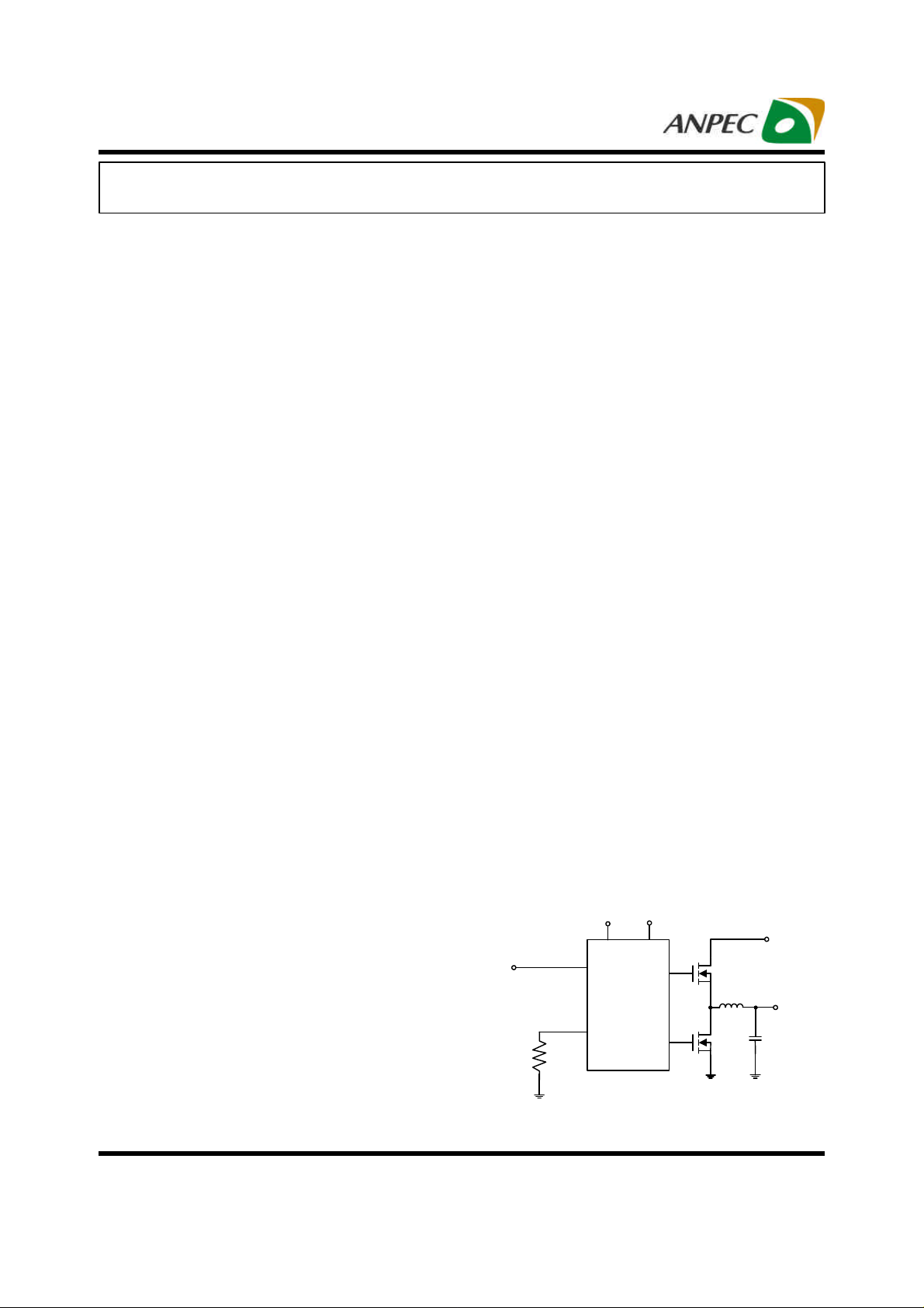
Simpilfied Application Circuit
V
+3V~25V
L
IN
V
OUT
FCCM
(Only QFN)
R
FSET
VCC=5V
APW7138
EN
Q1
Q2
www.anpec.com.tw1
Page 2
APW7138
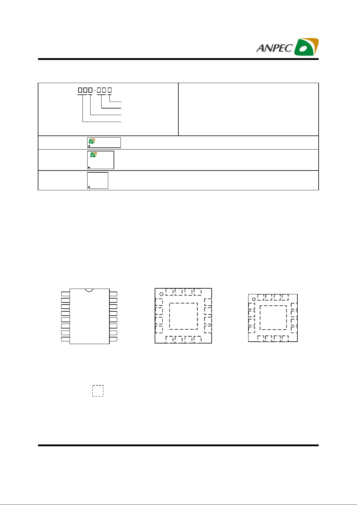
Ordering and Marking Information
APW7138
Assembly Material
Handling Code
Temperature Range
Package Code
APW7138 N :
APW7138 QA :
APW7138 QB :
Note: ANPEC lead-free products contain molding compounds/die attach materials and 100% matte tin plate termination finish; which
are fully compliant with RoHS. ANPEC lead-free products meet or exceed the lead-free requirements of IPC/JEDEC J-STD-020D for
MSL classification at lead-free peak reflow temperature. ANPEC defines “Green” to mean lead-free (RoHS compliant) and halogen
free (Br or Cl does not exceed 900ppm by weight in homogeneous material and total of Br and Cl does not exceed 1500ppm by
weight).
APW7138
XXXX
APW7138
XXXX
APW
7138
XXXX
Package Code
N : SSOP-16 QA: QFN4x4-16A QB: TQFN3x3-16
Operating Ambient Temperature Range
I : -40 to 85 oC
Handling Code
TR : Tape & Reel
Assembly Material
G : Halogen and Lead Free Device
XXXXX - Date Code
XXXXX - Date Code
XXXXX - Date Code
Pin Configuration
VIN
VCC
EN
NC
FB
GND
1
2
3
4
5
6
7
8
SSOP-16
(TOP VIEW)
16
UG
BOOT
15
PVCC
14
13
LG
12
PGND
ISEN
11
VO
10
9
FSET
= Thermal Pad (connected to GND plane for better heat dissipation)
PHASE
PGOOD
Copyright ANPEC Electronics Corp.
Rev. A.5 - Jul., 2010
VIN
VCC
FCCM
EN
1
2
3
4
PHASE
PGOOD
NC
UG
1516 14 13
Metal
GND Pad
(Bottem)
65 7 8
FB
FSET
QFN4x4-16A
(TOP VIEW)
BOOT
12
PVCC
11
LG
10
PGND
ISEN
9
VO
VIN
VCC
FCCM
EN
1
2
3
4
PHASE
UG
PGOOD
1516 14 13
Metal
GND Pad
(Bottem)
65 7 8
FB
NC
FSET
TQFN3x3-16
(TOP VIEW)
www.anpec.com.tw2
BOOT
12
PVCC
11
LG
PGND
10
ISEN
9
VO
Page 3
APW7138
Absolute Maximum Ratings (Note 1)
Symbol Parameter Rating Unit
VCC VCC Supply Voltage (VCC to GND) -0.3 ~ 7 V
V
PVCC Supply Voltage (PVCC to GND) -0.3 ~ 7 V
PVCC
VIN Input Power Voltage (VIN to GND) -0.3 ~28 V
V
BOOT Supply Voltage (BOOT to PHASE) -0.3 ~ 7 V
BOOT
V
V
V
Note 1: Absolute Maximum Ratings are those values beyond which the life of a device may be impaired. Exposure to absolute
maximum rating conditions for extended periods may affect device reliability.
BOOT Supply Voltage (BOOT to GND) -0.3 ~ 35 V
BOOT-GND
UG Voltage (UG to PHASE)
UG-PHASE
<400ns pulse width
>400ns pulse width
LG Voltage (LG to PGND)
LG-PGND
<400ns pulse width
>400ns pulse width
PHASE Voltage (PHASE to GND)
V
PHASE
<400ns pulse width
>400ns pulse width
V
PGND to GND Voltage -0.3 ~ 0.3 V
PGND
V
ISEN Supply Voltage (ISEN to GND) -0.3 ~ 28 V
ISEN
V
PGOOD Supply Voltage (PGOOD to GND) -0.3 ~ 7 V
PGOOD
V
All Other Pins (VO, FB, EN, FCCM and FSET to GND) -0.3 ~ VCC+0.3 V
I/O
-5 ~ V
-0.3 ~ V
BOOT
BOOT
+0.3
+0.3
-5 ~ VCC+0.3
-0.3 ~ VCC+0.3
-5 ~ 35
-2 ~ 28
TJ Maximum Junction Temperature 150
T
Storage Temperature Range -65 ~ 150
STG
T
Maximum Lead Soldering Temperature, 10 Seconds 260
SDR
V
V
V
°C
°C
°C
Thermal Characteristics (Note 2)
Symbol
Thermal Resistance -Junction to Ambient
θJA
Note 2: θJA is measured with the component mounted on a high effective thermal conductivity test board in free air. The exposed pad
of package is soldered directly on the PCB.
Parameter Typical Value Unit
SSOP-16
QFN4x4-16A
TQFN3x3-16
105
40
55
°C/W
Recommended Operating Conditions
Symbol Parameter Range Unit
VCC,V
Copyright ANPEC Electronics Corp.
Rev. A.5 - Jul., 2010
V
VIN
I
OUT
OUT
TA
TJ
VCC, PVCC Supply Voltage 4.5 ~ 5.5 V
PVCC
Converter Output Voltage 0.6 ~ 3.3 V
Converter Input Voltage 3 ~ 25 V
Converter Output Current 0 ~ 25 A
Ambient Temperature -40 ~ 85
Junction Temperature -40 ~ 125
www.anpec.com.tw3
o
C
o
C
Page 4
APW7138
Electrical Characteristics
Refer to the typical application circuits. These specifications apply over VCC=5V, VIN=7~25V and TA= -40 ~ 85 °C, unless
otherwise specified. Typical values are at TA=25°C.
Symbol
Parameter Test Conditions
SUPPLY CURRENT
I
VCC Input Bias Current VEN=5V, VFB=0.65V, VIN=7V to 25V - 1.7 2.5 mA
VCC
VCC Shutdown Current VEN=GND, VCC=5V - 0.1 1.0
PVCC Shutdown Current VEN=GND, V
I
VIN Input Bias Current
VIN
VEN=5V, VIN=7V - 6.5 10
VEN=5V, VIN=25V - 25 35
=5V - 0.1 1.0
PVCC
VIN Shutdown Current VEN=GND, VIN=25V - 0.1 1.0
POWER-ON-RESET (POR)
V
VCC_THR
Rising VCC POR Threshold Voltage 4.1 4.2 4.3 V
VCC POR Hysteresis - 0.2 - V
VOLTAGE REGULATION
V
Reference Voltage - 0.6 - V
REF
Regulation Accuracy Over Temperature -1 - +1 %
SWITCHING FREQUENCY
FSW Frequency Range DC Output Current 200 - 600 kHz
Frequency-Set-Accuracy
R
FSET
=44.5kΩ
PWM CONVERTERS
UG Minimum-Off Time Over temperature and VCC - 550 - ns
VO Pin Input Impedance V
= 3.3V - 134 -
OUT
IFB FB Input Bias Current VFB=0.6V -0.5 - +0.5
TSS Soft-Start Time VEN High to V
Regulation
OUT
(Note3)
- 1.5 - ms
Zero-Crossing Voltage Threshold -5 0 +5 mV
On-Time Ratio of PFM to PWM - 1.5 - -
POWER GOOD
R
I
PG_SS
R
I
PG_UV
R
PG_OV
R
PG_OC
I
PGOOD
PGOOD Pull-Down Impedance
I
PGOOD Leakage Current V
=5mA Sink (Soft-Start) 75 95 125
PGOOD
=5mA Sink (Under-Voltage) 75 95 125
PGOOD
=5mA Sink (Over-Voltage) 50 63 85
PGOOD
I
=5mA Sink (Over-Current) 25 32 45
PGOOD
=5V - 0.1 1.0
PGOOD
PGOOD Maximum Sink Current - 5.0 - mA
PGOOD Soft-Start Delay VEN High to V
High 2.20 2.75 3.30 ms
PGOOD
MOSFET GATE DRIVERS
UG Pull-Up Resistance V
UG Source Current V
UG Sink Resistance V
UG Sink Current V
=5V, IUG=0.1A - 1 2
BOOT
=5V, VUG-V
BOOT
=5V, IUG=0.1A - 1 2
BOOT
=5V, VUG-V
BOOT
=2.5V - 2 - A
PHASE
=2.5V - 2 - A
PHASE
APW7138
Min. Typ. Max.
Unit
µA
µA
µA
µA
µA
270 300 330 kHz
kΩ
µA
Ω
Ω
Ω
Ω
µA
Ω
Ω
Copyright ANPEC Electronics Corp.
www.anpec.com.tw4
Rev. A.5 - Jul., 2010
Page 5
APW7138
Electrical Characteristics (Cont.)
Refer to the typical application circuits. These specifications apply over VCC=5V, VIN=7~25V and TA= -40 ~ 85 °C, unless
otherwise specified. Typical values are at TA=25°C.
Symbol
Parameter Test Conditions
APW7138
Min. Typ. Max.
MOSFET GATE DRIVERS (CONT.)
LG Pull-Up Resistance V
LG Source Current V
LG Sink Resistance V
LG Sink Current V
=5V, ILG=0.1A - 1 2
PVCC
=5V, VLG-V
PVCC
=5V, ILG=0.1A - 0.6 1.2
PVCC
=5V, VLG-V
PVCC
=2.5V - 2 - A
PGND
=2.5V - 3 - A
PGND
TD Dead Time - 20 - ns
BOOTSTRAP DIODE
VF Forward Voltage V
PVCC-VBOOT-GND
=5V, IF=2mA - 0.8 - V
IR Reverse Leakage VR=25V - 0.2 -
CONTROL INPUTS
V
FCCMTHR
V
FCCMTHF
V
V
FCCM High Threshold 2.0 - - V
FCCM Low Threshold
EN High Threshold 2.0 - - V
ENR
EN Low Threshold - - 0.8 V
ENF
Only for QFN4x4-16A and
TQFN3x3-16 packages
- - 0.8 V
EN Leakage VEN=5V - 0.1 1.0
PROTECTION
IOC ISEN OCP Threshold I
ISC ISEN Short-Circuit Threshold I
Sourcing 20 26 30
SEN
Sourcing - 50 -
SEN
VUV UVP Threshold 65 70 75 %
UVP Debounce Interval - 2 -
V
OVP Rising Threshold 119 124 129 %
OVR
V
OVP Falling Threshold 99 104 109 %
OVF
OVP Debounce Interval - 2 -
T
OTP Rising Threshold
OTR
OTP Hysteresis
Note 3: Guaranteed by design.
(Note 3)
- 150 -
(Note 3)
- 25 -
Unit
Ω
Ω
µA
µA
µA
µA
µs
µs
o
C
o
C
Copyright ANPEC Electronics Corp.
www.anpec.com.tw5
Rev. A.5 - Jul., 2010
Page 6
APW7138
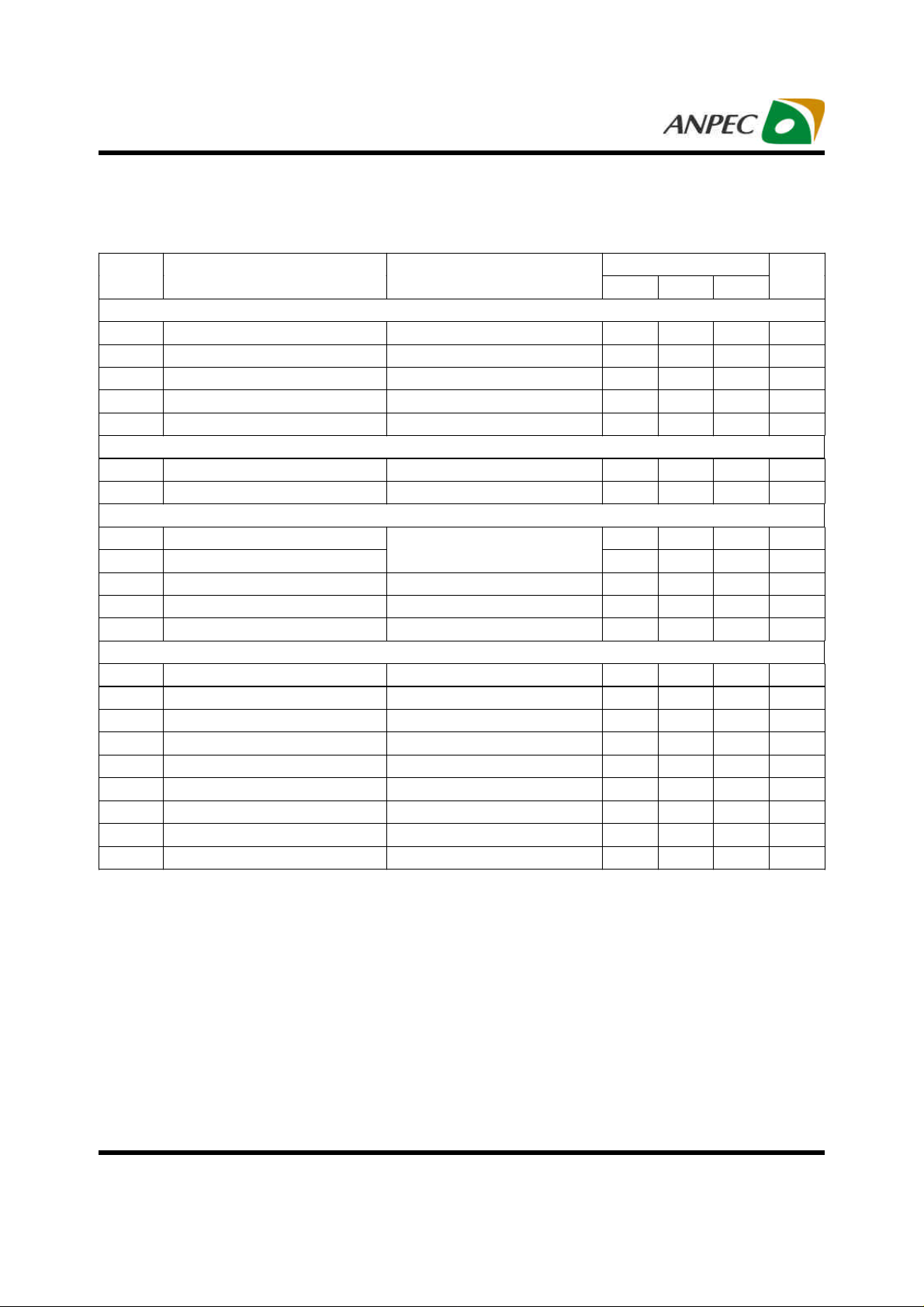
Typical Operating Characteristics
Output Voltage vs. Output Current
1.215
V
=1.2V
1.21
(V)
1.205
OUT
1.2
1.195
Output Voltage, V
1.190
1.185
OUT
V
=19V
IN1
V
=15V
IN1
V
=10V
IN1
0 1 2 3 4 5 6 7 8 9 10
Output Current, I
OUT
Reference Voltage Accuracy Over
Temperature
0.604
0.602
(V)
REF
0.6
0.598
(A)
Switching Frequency (300kHz)
345
335
325
(kHz)
SW
315
305
295
285
275
265
Switching Frequency, F
255
-40
Over Temperature
In PWM Mode
DC Output Current
-20 0 20 40
Junction Temperature, TJ (oC)
Switching Frequency vs. V
330
In PWM Mode
(kHz)
SW
320
310
300
290
DC Output Current
60 80 100 120 140
IN
0.596
Reference Voltage, V
0.594
-40 -20 0
20 40 60 80
Junction Temperature, TJ (oC)
Switching Frequency vs.
Ouput Current
350
300
(kHz)
250
SW
200
150
100
Switching Frequency, F
Copyright ANPEC Electronics Corp.
Rev. A.5 - Jul., 2010
V
=1.2V, I
OUT
50
0
0 1 2 3 4 5 6 7 8 9 10
Output Current, I
OUT
rising
OUT
(A)
100
120 140
280
Switching Frequency, F
270
5 7 9 11 13 15 17 19 21 23 25
Input Voltage, VIN (V)
www.anpec.com.tw6
Page 7
APW7138
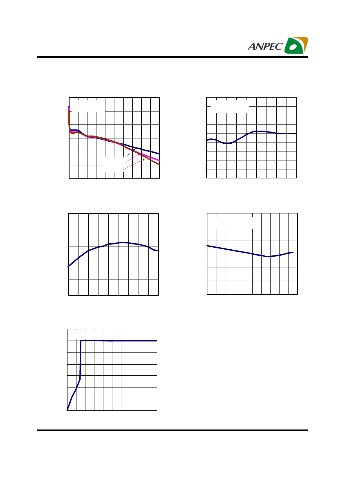
Operating Waveforms
Enable at Zero Initial Voltage of V
I
=5A
OUT
1
2
3
4
CH1: VEN (5V/div)
CH2: V
CH3: V
CH4: V
Time: 2ms/div
OUT
PGOOD
PHASE
(1V/div)
(5V/div)
(10V/div)
Shutdown at I
OUT
=5A
OUT
Enable Before End of Soft-Stop
No Load
1
2
3
4
CH1: VEN (5V/div)
CH2: V
CH3: V
CH4: V
Time: 2ms/div
OUT
PGOOD
PHASE
(1V/div)
(5V/div)
(10V/div)
Shutdown with Soft-Stop at No Load
1
2
3
4
CH1: VEN (5V/div)
CH2: V
CH3: V
CH4: V
Time: 5ms/div
OUT
PGOOD
PHASE
(1V/div)
(5V/div)
(10V/div)
Copyright ANPEC Electronics Corp.
Rev. A.5 - Jul., 2010
1
2
3
4
CH1: VEN (5V/div)
CH2: V
CH3: V
CH4: V
Time: 5ms/div
OUT
PGOOD
PHASE
(1V/div)
(5V/div)
(10V/div)
www.anpec.com.tw7
Page 8
APW7138
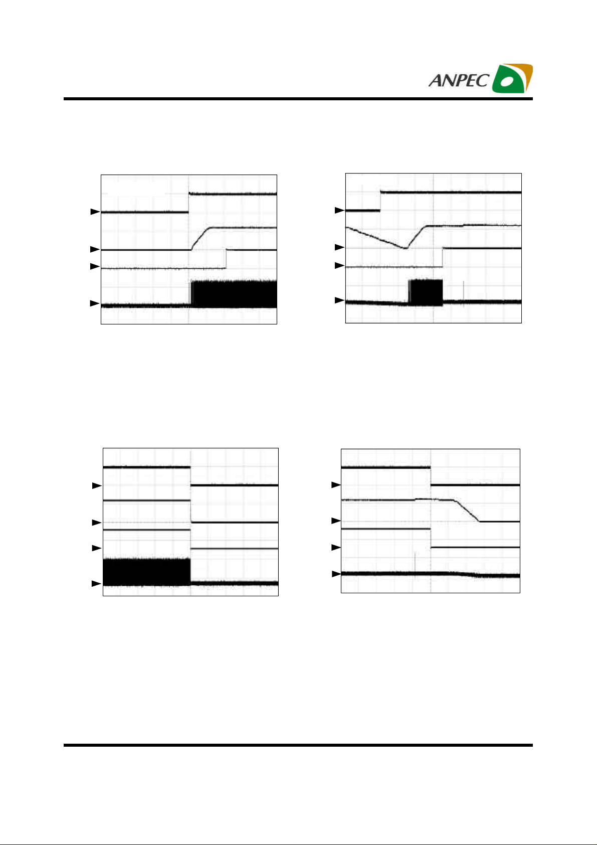
Operating Waveforms (Cont.)
Under-Voltage Protection
Short Circuit Test
1
2
3
4
CH1: IL (5A/div)
CH2: V
CH3: VLG (5V/div)
CH4: V
Time: 10µs/div
(20V/div)
UG
(1V/div)
OUT
Mode Transient From PWM to PFM
Mode Transient From PFM to PWM
I
=0.1A to 5A
OUT
1
2
3
4
CH1: V
CH2: V
CH3: V
CH4: IL (5A/div)
(5V/div)
PGOOD
(10V/div)
PHASE
(AC, 100mV/div)
OUT
Time: 10µs/div
Load Transient
0A->5A->0A
I
=5A to 0.1A
OUT
1
2
3
4
CH1: V
CH2: V
CH3: V
CH4: IL (5A/div)
(5V/div)
PGOOD
(10V/div)
PHASE
(AC, 100mV/div)
OUT
Time: 10µs/div
Copyright ANPEC Electronics Corp.
Rev. A.5 - Jul., 2010
I
OUT1
1
2
3
4
CH1: V
CH2: V
CH3: V
CH4: IL (5A/div)
Time: 50µs/div
rise/fall time=1us
(5V/div)
PGOOD
(10V/div)
PHASE
(AC, 100mV/div)
OUT
www.anpec.com.tw8
Page 9
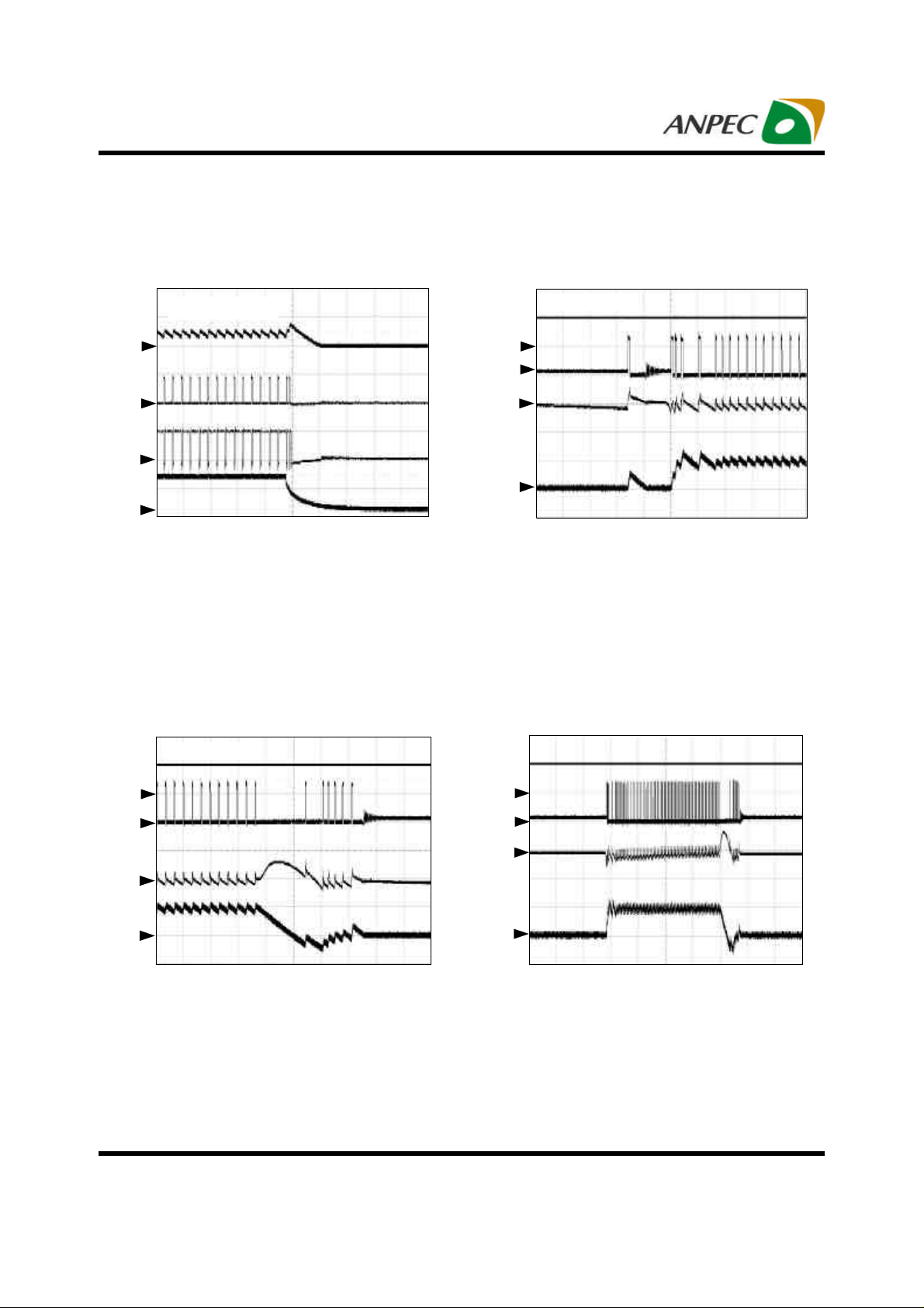
APW7138
Operating Waveforms (Cont.)
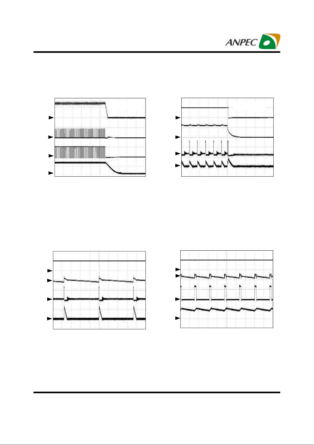
Over-Current Protection
1
2
3
4
CH1: IL (5A/div)
CH2: VUG (20V/div)
CH3: VLG (5V/div)
CH4: V
Time: 50µs/div
OUT
(1V/div)
Operating at Light Load of 100mA
I
rises slowly
OUT
1
2
3
4
CH1: V
CH2: V
CH3: V
CH4: IL (5A/div)
Time: 20µs/div
Short Circuit Test
In PFM Mode
(5V/div)
PGOOD
(1V/div)
OUT
(10V/div)
PHASE
Operating at Heavy Load of 5A
In PFM Mode
1
2
3
4
CH1: V
CH2: V
CH3: V
CH4: IL (2A/div)
(5V/div)
PGOOD
(AC, 100mV/div)
OUT1
(10V/div)
PHASE
Time: 20us/div
Copyright ANPEC Electronics Corp.
Rev. A.5 - Jul., 2010
1
2
3
4
CH1: V
CH2: V
CH3: V
CH4: IL (5A/div)
Time: 2µs/div
(5V/div)
PGOOD
(AC, 100mV/div)
OUT1
(10V/div)
PHASE
www.anpec.com.tw9
Page 10

APW7138
side MOSFET Source, output filter inductor and the
nnect +5V from the VCC pin to
the GND pin. Decoupling at least 1µF of a MLCC capacitor from the VCC pin
, and force PWM is disabled
Output voltage feedback pin. This pin is connected to the resistive divider that
signal to
rect measurement of the converter output voltage. The
+5V from the PVCC pin to the PGND pin. Decoupling at least 1µF of a MLCC
shift circuit. Connect
Pin Description
PIN
NO.
SSOP-16 QFN4x4-16A TQFN3x3-16
1 15 15 PHASE
2 16 16 PGOOD
3 1 1 VIN
4 2 2 VCC
- 3 3 FCCM
5 4 4 EN
6 5 5 NC No Connection.
NAME
Junction point of the highlow-side MOSFET Drain. Connect this pin to the Source of the high-side
MOSFET. PHASE serves as the lower supply rail for the UG high-side gate
driver.
The PGOOD pin is an open-drain output that indicates when the converter is
able to supply regulated voltage. Connect the PGOOD pin to +5V through a
pull-up resistor. The PGOOD pin has three distinct pull-down impedances
that correspond to an OVP (63Ω), OCP (32Ω), UVP (95Ω), and soft-start
(95Ω).
Battery voltage input pin. Connect this pin to the drain of the high-side
MOSFET.
Supply voltage input pin for control circuitry. Co
to the GND pin.
Selection pin for PWM controller to operate in either forced PWM or
automatic PWM/PFM mode. Force PWM mode is enable when FCCM pin is
pulled above the rising threshold voltage V
when the FCCM pin is pulled below the falling threshold voltage V
Enable pin of the PWM controller. The PWM is enabled when EN=1. When
the EN=0, the PWM is shutdown and only low leakage current is taken from
VCC and VIN.
FUNCTION
FCCMTHR
FCCMTHF
.
7 6 6 FB
8 Thermal Pad Thermal Pad GND Signal ground for the IC.
9 7 7 FSET
10 8 8 VO
11 9 9 ISEN
12 10 10 PGND
13 11 11 LG
14 12 12 PVCC
15 13 13 BOOT
16 14 14 UG
set the desired output voltage. The UVP and OVP circuits detect this
report output voltage status.
This pin is allowed to adjust the switching frequency. Connect a resistor R
from the FSET pin to the GND pin.
The VO pin makes a di
VO pin should be connected to the top feedback resistor at the converter
output.
Current sense pin. This pin is used to monitor the voltage drop across the
Drain and Source of the low-side MOSFET for over-current protection. For
precise current detection this input can be connected to the optional current
sense resistor placed in series with the Source of the low-side MOSFET.
Power ground of the LG low-side MOSFET driver. Connect the pin to the
Source of the low-side MOSFET.
Output of the low-side MOSFET driver. Connect this pin to Gate of the
low-side MOSFET. Swings from PGND to VCC.
Supply voltage input pin for the LG low-side MOSFET gate driver. Connect
capacitor from the PVCC pin to the PGND pin.
Supply Input for the UG Gate Driver and an internal levelto an external capacitor and diode to create a boosted voltage suitable to
drive a logic-level N-channel MOSFET.
Output of the high-side MOSFET driver. Connect this pin to Gate of the
high-side MOSFET.
FSET
Copyright ANPEC Electronics Corp.
Rev. A.5 - Jul., 2010
www.anpec.com.tw10
Page 11

APW7138
Block Diagram
GND
FB
VCC
EN
124% V
70% V
V
CC
V
REF
POR
VIN
REF
OV
UV
REF
Comparator
Digital
Soft-Start/Soft-Stop
Error
VO
PGOOD
60Ω 90Ω 30Ω
TON
Generator
Thermal
Shutdown
PWM
Frequency
Control
OC
LG
ISEN
I
SEN
V
CC
BOOT
UG
15k
PHASE
PVCC
PWM Signal Controller
LG
PGND
FSET
Typical Application Circuit
APW7138
PGOOD
R
PGOOD
1K
C
+5V
PVCC
1µF
R
VCC
2.2
C
VCC
1µF
Enable
Shutdown
PVCC
VCC
GND
EN1
VIN
UG
BOOT
PHASE
ISEN
LG
PGND
VO
FB
FSET
R
SEN
5.1K
C
BOOT
0.1µF
R
44.5K, 1%
FSET
Q1
APM4810
L
3.3µH
Q2
APM4810
OUT
C
IN
10µF
V
IN
3V~25V
C
OUT
150µFx2
R
GND
10K, 1%
V
OUT
1.2V
R
TOP
10K, 1%
Copyright ANPEC Electronics Corp.
Rev. A.5 - Jul., 2010
www.anpec.com.tw11
Page 12

APW7138
Function Description
Constant-On-Time PWM Controller with Input FeedForward
The constant-on-time control architecture is a pseudofixed frequency with input voltage feed-forward. This architecture relies on the output filter capacitor’s effective
series resistance (ESR) to act as a current-sense resistor,
so the output ripple voltage provides the PWM ramp signal.
In PFM operation, the high-side switch on-time controlled
by the on-time generator is determined solely by a oneshot whose pulse width is inversely proportional to input
voltage and directly proportional to output voltage. In PWM
operation, the high-side switch on-time is determined by
a switching frequency control circuit in the on-time generator block. The switching frequency control circuit
senses the switching frequency of the high-side switch
and keeps regulating it at a constant frequency in PWM
mode. This design improves the frequency variation to is
more outstanding than a conventional constant-on-time
controller which has large switching frequency variation
over input voltage, output current, and temperature. Both
in PFM and PWM, the on-time generator, which senses
input voltage on VIN pin, provides very fast on-time response to input line transients.
Another one-shot sets a minimum off-time (typical:
550ns). The on-time one-shot is triggered if the error comparator is high, the low-side switch current is below the
over-current threshold, and the minimum off-time oneshot has timed out.
Pulse-Frequency Modulation (PFM) Mode
In PFM mode, an automatic switchover to pulse-frequency
modulation (PFM) tak es place at light loads. This
switchover is affected by a comparator that truncates the
low-s ide switch on-time at the inductor current zero
crossing. This mechanism causes the threshold between
PFM and PWM operations to coincide with the boundary
between continuous and discontinuous inductor-current
operation (also known as the critical conduction point).
The on-time of PFM mode is designed as 1.5 time of the
nominal on-time of PWM mode. The on-time of PFM is
given by:
OUT
V
T ×=−
PFMON
5.1
IN
SW
V
F
Where FSW is the nominal switching frequency of the converter in PWM mode.
This design provides a hysteresis of converter output
current to prevent wrong or repeatedly PFM/PWM handoff
with constant output current. The load current at handoff
from PFM to PWM mode is given by:
OUTIN
I
LOAD(PFM to PWM)
1
2
=
VV
−
×=
L
OUTIN
VV
−
L2
T
×
ON-PFM
OUT
V
5.1
××
IN
SW
V
F
The load current at handoff from PWM to PFM mode is
given by:
OUTIN
I
LOAD(PWM to PFM)
Therefore, the I
1
2
=
LOAD(PFM to PWM)
VV
−
×=
VV
−
L2
×
L
OUTIN
T
1
SW
F
is 1.5 time of the I
ON-PWM
OUT
V
××
IN
V
LOAD(PWM to PFM)
Forced-PWM Mode (Only for QFN4x4-16A and TQFN3x316 Packages)
The Forced-PWM mode disables the zero-crossing comparator which truncates the low-side switch on-time at
the inductor current zero cross ing. This causes the lowside gate-drive waveform to become the complement of
the high-s ide gate-drive waveform. This in turn causes
the inductor current to rev erse at light loads while UG
maintains a duty factor of V
. The benefit of Forced-
OUT/VIN
PWM mode is to k eep the switching frequency fairly
constant. The Forced-PWM mode is the most useful for
reducing audio frequency noise, improving load-transient
response, and providing s ink-current capability for dynamic output voltage adjustment.
Power-On-Reset
A Power-On-Reset (POR) function is designed to prevent
wrong logic controls when the VCC v oltage is low. The
POR function continually monitors the bias supply voltage on the VCC pin if at least one of the enable pins is set
high. When the rising VCC voltage reaches the rising POR
voltage threshold (4.2V typical), the POR signal goes high
and the chip initiates soft-start operations. When this voltage drop lower than 4V (typical), the POR disables the
chip.
.
Copyright ANPEC Electronics Corp.
Rev. A.5 - Jul., 2010
www.anpec.com.tw12
Page 13

APW7138
Function Description (Cont.)
Enable Control
When the EN pin is high (EN=1), the PWM is enabled and
the soft-start is initiated. When EN is low (EN=0), the chip
is in the shutdown mode and only low leakage current is
taken from VCC and VIN. In shutdown mode, LG will be
pulled high.
Soft-Start and Soft-Stop
The APW7138 integrates digital soft-start/soft-stop circuits to ramp up/down the output voltage of the converter
to the programmed regulation setpoint at a predictable
slew rate. The slew rate of output voltage is internally
controlled to limit the inrush current through the output
capacitors during soft-start process. The figure 1 shows
soft-start sequence. When the EN pin is pulled above the
rising EN threshold voltage, the device initiates a softstart process to ramp up the output voltage. The soft-start
interval is 1.5ms (ty pical) and independent of the UG
switching frequency.
2.75ms
V
and V
CC
1.5ms
EN
PVCC
V
OUT
In the event of under-voltage or EN shutdown, the chip
enables the soft-stop function. At light load, the soft-stop
gradually ramps down the output voltage, following the
internal falling soft-stop voltage, by controlling the lowside MOSFET working as a sinking linear regulator. At
heavy load, the soft-stop will not regulate the output voltage if the output voltage is below the falling soft-stop
regulation voltage level. The soft-stop process, which
takes about 3 times of the time from VEN high to V
PGOOD
high, is completed when the internal counter finishes
counting. At this moment, the LG goes high level with
latch. Cycling the EN signal or VCC power-on-reset signal can reset the latch.
Under-Voltage Protection (UVP)
In the process of operation, if a short-circuit occurs, the
output voltage will drop quickly. The under-voltage continually monitors the VFB voltage after soft-start process is
completed. If a load step is strong enough to pull the
output voltage lower than the under-voltage threshold,
PGOOD pin will pull down to 95Ω immediately and start a
soft-stop process to shut down the output. The undervoltage threshold is 70% of the normal output voltage.
The under-voltage comparator has a built-in 2µs noise
filter to prevent the chip from wrong UVP shutdown caused
by noise. Toggling EN pin to low, or recycling VCC, will
clear the latch and bring the chip back to operation.
V
PGOOD
Figure 1. Soft-Start Sequence
During soft-start stage before the PGOOD pin is ready,
the under-voltage protection is prohibited. The over-voltage and over-current protection functions are enabled. If
the output capacitor has residue voltage before start-up,
both low-side and high-side MOSFETs are in off-state
until the internal digital soft start voltage equal the V
voltage, which ensures the output voltage starts from its
existing voltage level.
Copyright ANPEC Electronics Corp.
Rev. A.5 - Jul., 2010
Over-Voltage Protection (OVP)
The over-voltage function monitors the output voltage by
FB pin. When the V
voltage increase over 124% of the
FB
reference voltage due to the high-side MOSFET failure or
for other reasons, the over-voltage protection comparator is designed with a 2µs noise filter will force the lowside MOSFET gate driver to be high. This action actively
pulls down the output voltage. When the OVP occurs, the
PGOOD pin will pull down to 63Ω and latch-off the
converter. This OVP scheme only clamps the voltage overshoot and doesn’t invert the output voltage when otherwise activated with a continuously high output from lowside MOSFET driver. It’s a common problem for OVP
FB
schemes with a latch. The OVP fault will remain latched
until cycling the EN signal or VCC power-on-reset signal.
www.anpec.com.tw13
Page 14

APW7138
Function Description (Cont.)
Power Good Indicator
The APW7138 features an open-drain PGOOD output pin
to indicate one of the IC’s working statuses including
soft-start, under-voltage fault, over-current fault, and overvoltage faule. The unique fault-identification capability can
drastically reduce trouble-shooting time and effort.
The pull-down resistance of the PGOOD pin corresponds
to the fault status of the controller. During soft-start or if
an under voltage fault occurs, the PGOOD pull-down resistance is 95Ω, or 32Ω for an over current fault, or 63Ω
for an over voltage fault. The pull-low resistance is undefined if VCC is below the rising/falling POR threshold.
Over-Temperature Protection (OTP)
When the junction temperature increases above the rising threshold temperature TOTR, the IC will enter the
over-temperature protection (OTP) state that suspends
the PWM, which forces the LG and UG gate drivers to
output low voltages. The status of the PGOOD pin does
not change, nor does the converter latch-off. The thermal
sensor allows the converters to start a start-up process
and regulate the output voltage again after the junction
temperature cools by 25oC. The OTP is designed with a
25oC hysteresis to lower the average TJ during continuous thermal overload conditions, which increases lifetime of the APW7138.
Over-Current Protection (OCP) and Short-Circuit Protection (SCP)
The over-current protection (OCP) is designed to resist
the slow slew rate load current; on the other hand, the
short-circuit protection (SCP) is used to take care of rapid
shorted output. The setpoint for OCP and SCP is programmed with resistor R
that is connected across the
SEN
ISEN pin and drain of the low-side MOSFET. The SCP
setpoint is internally set to twice the OCP setpoint.
The inductor current develops a negative voltage across
the R
of the low-side MOSFET that is sampled and
DS(ON)
held shortly before LG gate-driver output goes low. The
OCP fault occurs if I
rises above the OCP threshold
SEN
current IOC (typical :26µA) while attempting to null the nega-
tive voltage across the PHASE and GND pins. When the
I
exceeds IOC, the OCP counter starts to work.
SEN
Meanwhile, pulses on all the PWM (I
20µs, the OCP will be triggered. When I
> IOC) remains for
SEN
falls below I
SEN
on a PWM puls es before 20µs has elapsed, the counter
will be reset. The SCP fault will occur within 10 µs when
I
exceeds twice IOC. The relationship between the
SEN
sampled current and MOSFET current is given by:
L)ON(DSSENSEN IRRI ×=×
Which means the current sensing pin will source current
to make the voltage drop on the MOSFET and is equal to
the voltage generated on the sensing resistor along the
ISEN pin current flowing path.
In the formula, the value of R
SEN
R×=
IR
OC
I
is then written as:
SEN
)OC(OUT)ON(DS
where:
- R
is the resistor used to program the over-current
SEN
setpoint.
- I
- IOC is the I
is the desired overcurrent setpoint, the setting
OUT(OC)
value is close to the continuous DC load current I
threshold current sourced from the ISEN
SEN
OUT
.
pin that will activate the OCP circuit. The typical value is
26µA.
When the OCP or SCP fault is detected, the PGOOD pin
will pull down to 32Ω and latch off the converter. The fault
will remain latched until the EN pin has been pulled below the falling EN threshold voltage or if VCC has decayed
below the falling POR threshold voltage.
I
PEAK
I
OUT
I
VALLEY
INDUCTOR CURRENT
0
Time
Figure 2. Over-Current Algorithm
Programming the PWM Switching Frequency
The APW7138 does not use a clock signal to produce
PWM. The resistor R
that is connected from the FSET
FSET
pin to the GND pin programs the PWM switching frequency
OC
Copyright ANPEC Electronics Corp.
Rev. A.5 - Jul., 2010
www.anpec.com.tw14
Page 15

APW7138
Function Description (Cont.)
Programming the PWM Switching Frequency (Cont.)
FSW. The approximate PWM switching frequency is written as:
SW
F×=
Where:
- FSW is the PWM switching frequency
- R
FSET
- K = 75 x 10
1
FSET
RK
is the FSW programming resistor
-12
Copyright ANPEC Electronics Corp.
Rev. A.5 - Jul., 2010
www.anpec.com.tw15
Page 16

APW7138
TOP
GND
Application Information
Output Voltage Setting
The output voltage is adjustable from 0.6V to 3.3V
with a resistor-divider connected with FB, GND, and
converter’s output. Using 1% or better resistors for the
resistor-divider is recommended. The output voltage is
determined by:
V0.61
=×+
OUT
Where 0.6 is the reference voltage, R
connected from converter’s output to FB, and R
resistor connected from FB to GND. Suggested R
R
R
is the resistor
TOP
is the
GND
is
GND
in the range from 1K to 20kΩ. To prevent stray pickup,
locate resistors R
TOP
and R
close to APW7138.
GND
Output Inductor Selection
The duty cycle (D) of a buck converter is the function of
the input voltage and output voltage. Once an output voltage is fixed, it can be written as:
V
OUT
D =
V
IN
The inductor value (L) determines the inductor ripple
current, I
, and affects the load transient reponse.
RIPPLE
Higher inductor value reduces the inductor’s ripple current and induces lower output ripple voltage. The ripple
current and ripple voltage can be approximated by:
OUT
OUTIN
V- V
RIPPLE
I ×
=
SW
V
IN
V
LF
×
Where FSW is the switching frequency of the regulator.
Although the inductor value and frequency are increased
and the ripple current and voltage are reduced, there is a
tradeoff exists between the inductor’s ripple current and
the regulator load transient response time.
A smaller inductor will give the regulator a faster load
transient response at the expense of higher ripple current.
Increasing the switching frequency (FSW) also reduces
the ripple current and voltage, but it will increase the
switching loss of the MOSFETs and the power dissipation of the converter. The maximum ripple current occurs
at the maximum input voltage. A good starting point is to
choose the ripple current to be approximately 30% of the
maximum output current. Once the inductance value has
been chosen, selecting an inductor that is capable of carrying the required peak current without going into
saturation. In some types of inductors, espec ially core
that is made of ferrite, the ripple current will increase
abruptly when it saturates. This results in a larger output
ripple voltage.
Output Capacitor Selection
Output voltage ripple and the transient voltage deviation
are factors that have to be taken into consideration when
selecting an output capacitor. Higher capacitor value and
lower ESR reduce the output ripple and the load transient drop. Therefore, selecting high performance low
ESR capacitors is recommended for switching regulator
applications. In addition to high frequency noise related
to MOSFET turn-on and turn-off, the output voltage ripple
includes the capacitance voltage drop ∆V
voltage drop ∆V
caused by the AC peak-to-peak
ESR
and ESR
COUT
inductor’s current. These two voltages can be represented
by:
RIPPLE
I
OUTC
V
=∆
RIPPLEESR
SWOUT
F8C
ESR
RIV
×=∆
These two components constitute a large portion of the
total output voltage ripple. In some applications, multiple
capacitors have to be parallelled to achieve the desired
ESR value. If the output of the converter has to support
another load with high pulsating current, more capacitors are needed in order to reduce the equivalent ESR
and suppress the voltage ripple to a tolerable level. A
small decoupling capacitor in parallel for bypassing
the noise is also recommended, and the voltage rating
of the output capacitors are also must be considered.
To support a load transient that is faster than the
switching frequency, more capacitors are needed for
reducing the voltage excursion during load step change.
Another aspect of the capacitor selection is that the
total AC current going through the capacitors has to be
less than the rated RMS current specified on the capacitors in order to prevent the capacitor from overheating.
Copyright ANPEC Electronics Corp.
Rev. A.5 - Jul., 2010
www.anpec.com.tw16
Page 17

APW7138
Application Information (Cont.)
Input Capacitor Selection
The input capacitor is chosen based on the voltage rating
and the RMS current rating. For reliable operation, selecting the capacitor voltage rating to be at least 1.3 times
higher than the maximum input voltage. The maximum
RMS c urrent rating requirement is approximately I
where I
is the load current.
OUT
OUT
/2,
During power up, the input capacitors have to handle great
amount of surge current. For low-duty notebook
appliactions, ceramic capacitor is recommended. The capacitors must be connected between the drain of highside MOSFET and the source of low-side MOSFET with
very low-impeadance PCB layout.
MOSFET Selection
The applic ation for a notebook battery with a maximum
voltage of 24V, at least a minimum 30V MOSFETs should
be used. The design has to trade off the gate charge with
the R
of the MOSFET:
DS(ON)
• For the low-side MOSFET, before it is turned on, the
body diode has been conducting. The low-side MOSFET
driver will not charge the miller capacitor of this MOSFET.
• In the turning off process of the low-side MOSFET, the
load current will shift to the body diode first. The high dv/
dt of the phase node voltage will charge the miller capacitor through the low-side MOSFET driver sinking current
path. This results in much less switching loss of the lowside MOSFETs. The duty cycle is often very small in high
battery voltage applications, and the low-side MOSFET
will conduct most of the switching cycle; therefore, when
using smaller R
verter can reduce power loss. The gate charge for this
MOSFET is usually of secondary consideration. The highside MOSFET does not have this zero voltage switching
condition; in addition, becaus e it conducts for less time
compared to the low-side MOSFET, the switching loss
tends to be dominant. Priority should be given to the
MOSFETs with les s gate charge, so that both the gate
driver loss, and switching loss, will be minimized.
The selection of the N-channel power MOSFETs are determined by the R
(C
) and maximum output current requirement. The
RSS
losses in the MOSFETs have two components: conduc-
of the low-side MOSFET, the con-
DS(ON)
, reversing transfer capacitance
DS(ON)
tion loss and transition loss. For the high-side and lowside MOSFETs, the losses are approximately given by
the following equations:
P
= I
high-side
P
low-side
= I
OUT
OUT
2(1+ TC)(R
2(1+ TC)(R
DS(ON)
DS(ON)
)D + (0.5)( I
)(1-D)
)(VIN)( tSW)F
OUT
SW
Where
I
is the load current
OUT
TC is the temperature dependency of R
DS(ON)
FSW is the switching frequency
tSW is the switching interval
D is the duty cycle
Note that both MOSFETs have conduction losses while
the high-side MOSFET includes an additional transition
loss. The switching interval, tSW, is the function of the reverse transfer capacitance C
factor in the temperature dependency of the R
can be extracted from the “R
. The (1+TC) term is a
RSS
vs. Temperature” curve
DS(ON)
DS(ON)
and
of the power MOSFET.
Layout Consideration
In any high switching frequency converter, a correct layout is important to ensure proper operation of the
regulator. With power devices switching at higher
frequency, the resulting current transient will cause voltage spike across the interconnecting impedance and
parasitic circuit elements. As an example, consider the
turn-off transition of the PWM MOSFET. Before turn-off
condition, the MOSFET is carrying the full load current.
During turn-off, current stops flowing in the MOSFET and
is freewheeling by the low side MOSFET and parasitic
diode. Any parasitic inductance of the circuit generates a
large voltage spike during the switching interval. In
general, using short and wide printed circuit traces should
minimize interconnecting impedances and the magnitude of voltage spike. Besides, signal and power grounds
are to be kept separate and finally combined using ground
plane construction or single point grounding. The best
tie-point between the signal ground and the power ground
is at the negative side of the output capacitor on each
channel, where there is less noise. Noisy traces beneath
the IC are not recommended. Below is a checklist for
your layout:
Copyright ANPEC Electronics Corp.
Rev. A.5 - Jul., 2010
www.anpec.com.tw17
Page 18

APW7138
Application Information (Cont.)
Layout Consideration (Cont.)
• Keep the switching nodes (UG, LG, BOOT, PHASE,
and ISEN) away from sensitive small s ignal nodes since
these nodes are fast moving signals.Therefore, keep
traces to these nodes as short as poss ible and there
should be no other weak signal traces in parallel with
theses traces on any layer.
• The s ignals going through theses traces have both
high dv/dt and high di/dt with high peak charging and discharging current. The traces from the gate drivers to the
MOSFETs (UG, LG) should be short and wide.
• Place the source of the high-side MOSFET and the
drain of the low-side MOSFET as close as possible. Minimizing the impedance with wide layout plane between
the two pads reduces the voltage bounc e of the node. In
addition, the large layout plane between the drain of the
MOSFETs (VIN and PHASE nodes) can get better heat
sinking.
• For accurate current sensing, the ISEN trace should be
a separate trace and independently go to the drain terminal of the low s ide MOSFET. The PGND is the current
sensing circuit reference ground and also the power
ground of the LG low-side MOSFET. On the hand, the
PGND trace should be a separate trace and independently go to the source of the low-side MOSFET. Besides,
the current sense resistor should be close to ISEN pin to
avoid parasitic capacitor effect and noise coupling.
• Decoupling capacitors, the resistor-divider, and boot
capacitor should be close to their pins. (For example, place
the decoupling ceramic capacitor close to the drain of the
high-side MOSFET as close as possible).
• The input bulk capacitors should be close to the drain
of the high-side MOSFET, and the output bulk capacitors
should be close to the loads. The input capacitor’s ground
should be close to the grounds of the output capacitors
and low-side MOSFET.
• Locate the resistor-divider close to the FB pin to mini-
mize the high impedance trace. In addition, FB pin traces
can’t be close to the switching signal traces (UG, LG,
BOOT, PHASE, and ISEN).
0.5mm*
0.65mm 0.3mm
0.5mm*
0.24mm
0.5mm
16 15 14 13
5.59mm
1 2 3 4
0.635mm
2.3mm
0.508mm
QFN4x4-16A
0.508mm
TQFN3x3-16
12 11
SSOP-16
4mm
2.3mm
3mm
1.66mm
1.66mm
5
0.254mm
10 9
7 8
6
0.342mm
* Just Recommend
0.162mm
* Just Recommend
1.625mm
4mm
3mm
Copyright ANPEC Electronics Corp.
Rev. A.5 - Jul., 2010
Figure 3. Rec ommended Minimum Footprint
www.anpec.com.tw18
Page 19

APW7138
Pack age Information
SSOP-16
D
SEE VIEW A
E1
E
h X 45
L
INCHES
0.025 BSC
o
c
θ
0.069
0.197
0.244
0.157
o
8
be
A2
A
A1
VIEW A
1.75
0.25
5.00
6.20
4.00
8
o
SSOP-16
MIN. MAX.
0.004 0.010
0.049
0.008 0.012
0.006 0.010
0.189
0.228
0.150
0.016 0.050
0.010 0.020
0
S
Y
M
B
O
L
A
A2
b
c
D
E
E1
e
L
h
θ
Note: 1. Follow JEDEC MO-137 AB.
2. Dimension "D" does not include mold flash, protrusions or gate burrs.
Mold flash, protrusion or gate burrs shall not exceed 6 mil per side.
3. Dimension "E" does not include inter-lead flash or protrusions.
Inter-lead flash and protrusions shall not exceed 10 mil per side.
MILLIMETERS
MIN. MAX.
0.10A1
1.24
0.20 0.30
0.15 0.25
4.80
5.80
3.80
0.635 BSC
0.40 1.27
0.25 0.50
o
0
0.25
GAUGE PLANE
SEATING PLANE
Copyright ANPEC Electronics Corp.
Rev. A.5 - Jul., 2010
www.anpec.com.tw19
Page 20

APW7138
Pack age Information
QFN4x4-16A
D
Pin 1
D2
Pin 1 Corner
A
E
b
A1
A3
E2KL
S
Y
M
B
O
L
A
A1
A3
b
D
D2
E
E2
e
L
K
Copyright ANPEC Electronics Corp.
Rev. A.5 - Jul., 2010
MIN. MAX.
0.80
0.00
0.25 0.35
3.90 4.10
2.10 2.50
3.90 4.10
2.10
0.30 0.50
0.20
e
QFN4x4-16A
MILLIMETERS
1.00
0.05
0.20 REF
2.50
0.65 BSC 0.026 BSC
INCHES
MIN. MAX.
0.031
0.000
0.008 REF
0.010 0.014
0.154 0.161
0.083 0.098
0.154 0.161
0.083
0.012 0.020
0.008
0.039
0.002
0.098
www.anpec.com.tw20
Page 21

APW7138
Pack age Information
TQFN3x3-16
D
A
A
A1
A3
b
D
D2
E
E2
e
L
K
E
Pin 1
D2
Pin 1
Corner
e
S
Y
M
B
O
L
MILLIMETERS
MIN. MAX.
0.70
0.00
0.20 REF
0.18 0.30
2.90 3.10
1.50 1.80
2.90 3.10
1.50
0.50 BSC 0.020 BSC
0.30 0.50
0.20
TQFN3x3-16
0.80
0.05
1.80
E2
k
INCHES
MIN. MAX.
0.028
0.000
0.008 REF
0.007 0.012
0.114 0.122
0.059 0.071
0.114 0.122
0.059
0.012 0.020
0.008
b
A1
A3
0.031
0.002
0.071
Copyright ANPEC Electronics Corp.
Rev. A.5 - Jul., 2010
Note : Follow JEDEC MO-220 WEED-4.
www.anpec.com.tw21
Page 22

APW7138
0.00
0.00
Carrier Tape & R eel Dimensions
OD0
B0
P0
P2
P1
A
E1
F
W
Application
SSOP-16
Application
QFN4x4-16A
Application
TQFN3x3-16
K0
SECTION A-A
B
A
H
A0
SECTION B-B
OD1
B
T
A
d
T1
A H T1 C d D W E1 F
330.0±2.00 50 MIN.
12.4+2.00
-
13.0+0.50
-0.20
1.5 MIN. 20.2 MIN. 12.0±0.30 1.75±0.10 5.50±0.10
P0 P1 P2 D0 D1 T A0 B0 K0
4.00±0.10 8.00±0.10 2.00±0.05
1.5+0.10
-0.00
1.5 MIN.
0.6+0.00
-0.40
6.40±0.20 5.20±0.20 2.10±0.20
A H T1 C d D W E1 F
330.0±2.00 50 MIN.
12.4+2.00
-
13.0+0.50
-0.20
1.5 MIN. 20.2 MIN. 12.0±0.30 1.75±0.10 5.5±0.05
P0 P1 P2 D0 D1 T A0 B0 K0
4.0±0.10 8.0±0.10 2.0±0.05
1.5+0.10
-0.00
1.5 MIN.
0.6+0.00
-0.40
4.30±0.20 4.30±0.20 1.30±0.20
A H T1 C d D W E1 F
330±2.00 50 MIN.
12.4+2.00
-0.00
13.0+0.50
-0.20
1.5 MIN. 20.2 MIN. 12.0±0.30 1.75±0.10 5.5±0.05
P0 P1 P2 D0 D1 T A0 B0 K0
4.0±0.10 8.0±0.10 2.0±0.05
1.5+0.10
-0.00
1.5 MIN.
0.6+0.00
-0.40
3.30±0.20 3.30±0.20 1.30±0.20
Copyright ANPEC Electronics Corp.
Rev. A.5 - Jul., 2010
(mm)
www.anpec.com.tw22
Page 23

APW7138
Devices Per Unit
Package Type Unit Quantity
SSOP-16
QFN4x4-16A
TQFN3x3-16
Taping Direction Information
SSOP-16
Tape & Reel 2500
Tape & Reel 3000
Tape & Reel 3000
USER DIRECTION OF FEED
QFN4x4-16A
Copyright ANPEC Electronics Corp.
Rev. A.5 - Jul., 2010
USER DIRECTION OF FEED
www.anpec.com.tw23
Page 24

APW7138
Taping Direction Information (Cont.)
TQFN3x3-16
USER DIRECTION OF FEED
Classification Profile
Copyright ANPEC Electronics Corp.
Rev. A.5 - Jul., 2010
www.anpec.com.tw24
Page 25

APW7138
Classification Reflow Profiles
Profile Feature Sn-Pb Eutectic Assembly Pb-Free Assembly
Preheat & Soak
Temperature min (T
Temperature max (T
Time (T
smin
to T
smax
smin
smax
) (ts)
)
)
Average ramp-up rate
(T
to TP)
smax
Liquidous temperature (TL)
Time at liquidous (tL)
Peak package body Temperature
(Tp)*
Time (tP)** within 5°C of the specified
classification temperature (Tc)
Average ramp-down rate (Tp to T
smax
Time 25°C to peak temperature
See Classification Temp in table 1 See Classification Temp in table 2
)
100 °C
150 °C
60-120 seconds
150 °C
200 °C
60-120 seconds
3 °C/second max. 3°C/second max.
183 °C
60-150 seconds
217 °C
60-150 seconds
20** seconds 30** seconds
6 °C/second max. 6 °C/second max.
6 minutes max. 8 minutes max.
* Tolerance for peak profile Temperature (Tp) is defined as a supplier minimum and a user maximum.
** Tolerance for time at peak profile temperature (tp) is defined as a supplier minimum and a user maximum.
Table 1. SnPb Eutectic Process – Classification Temperatures (Tc)
Package
Thickness
<2.5 mm
Volume mm
3
Volume mm
<350
235 °C 220 °C
≥350
3
≥2.5 mm 220 °C 220 °C
Table 2. Pb-free Process – Classification Temperatures (Tc)
Package
Thickness
<1.6 mm
1.6 mm – 2.5 mm
Volume mm3
<350
Volume mm3
350-2000
Volume mm3
260 °C 260 °C 260 °C
260 °C 250 °C 245 °C
>2000
≥2.5 mm 250 °C 245 °C 245 °C
Reliability Test Program
Test item Method Description
SOLDERABILITY JESD-22, B102
HOLT JESD-22, A108
PCT JESD-22, A102
TCT JESD-22, A104
HBM MIL-STD-883-3015.7
MM JESD-22, A1 15
Latch-Up JESD 78
Copyright ANPEC Electronics Corp.
Rev. A.5 - Jul., 2010
5 Sec, 245°C
1000 Hrs, Bias @ Tj=125°C
168 Hrs, 100%RH, 2atm, 121°C
500 Cycles, -65°C~150°C
VHBM≧2KV
VMM≧200V
10ms, 1tr≧100mA
www.anpec.com.tw25
Page 26

APW7138
Customer Service
Anpec Electronics Corp.
Head Office :
No.6, Dusing 1st Road, SBIP,
Hsin-Chu, Taiwan, R.O.C.
Tel : 886-3-5642000
Fax : 886-3-5642050
Taipei Branch :
2F, No. 11, Lane 218, Sec 2 Jhongsing Rd.,
Sindian City, Taipei County 23146, Taiwan
Tel : 886-2-2910-3838
Fax : 886-2-2917-3838
Copyright ANPEC Electronics Corp.
Rev. A.5 - Jul., 2010
www.anpec.com.tw26
Page 27

 Loading...