

Page 1
APW7057
High Power Step-Down Synchronous DC/DC Controller
Features
••
Operates from +5V Input
•
••
••
0.8V Internal Reference Voltage
•
••
- ±1.5% Accuracy Over Line, Load and Temp.
••
0.8V to VCC Output Range
•
••
••
Full Duty Cycle Range
•
••
- 0% to 100%
••
Internal Loop Compensation
•
••
••
Internal Soft Start
•
••
- Typical 2ms
••
• Programmable Over-Current Protection
••
- Lossless Sensing Using MOSFET R
••
• Under-Voltage Protection
••
••
• Drives External N-Channel MOSFETs
••
••
• Shutdown Control
••
••
• Small SOP-8 Package
••
DS (ON)
Applications
••
• Motherboard
••
••
• Graphics Cards
••
••
• Cable or DSL Modems, Set Top Boxes
••
••
• DSP Supplies
••
General Description
The APW7057 is a 300kHz constant frequency voltage mode synchronous switching controller that drives
external N-channel MOSFETs. When the input supply drops close to output, the upper MOSFET remains
on, achieving 100% duty cycle. Internal loop compensation is optimized for fast transient response, eliminating external compensation network. The precision
0.8V reference makes this part suitable for a wide variety of low voltage applications. Soft start is internally
set to 2ms, limiting the input in-rush current and preventing the output from overshoot during powering up.
The APW7057 has over current and short circuit
protections. Over current protection is achieved by
monitoring the voltage drop across the high side
MOSFET, eliminating the need for a current sensing resistor and short circuit condition is detected
through the FB pin. If either fault conditions occur,
the APW7057 would initiate the soft start cycle. After
three cycles and if the fault condition persists, the
controller will be shut down. To restart the controller ,
either recycle the V
OSCSET pin below 1.25V.
The APW7057 can be shutdown by pulling the OCSET
pin below 1.25V. In shutdown, both gate drive signals
will be low. The controller is available in a small SOP8 package.
supply or momentarily pull the
CC
••
• Memory Supplies
••
••
• 5V Input DC-DC Regulators
••
••
• Distributed Power Supplies
••
ANPEC reserves the right to make changes to improve reliability or manufacturability without notice, and
advise customers to obtain the latest version of relevant information to verify before placing orders.
Copyright ANPEC Electronics Corp.
Rev. A.3 - Oct., 2003
Pinouts
BOOT
UGATE
GND
LGATE
1
2
3
4
SOP-8 (Top View )
8
7
6
5
www.anpec.com.tw1
PHASE
OCSET
FB
VCC
Page 2
APW7057
Ordering and Marking Information
APW 7057
APW7057 K :
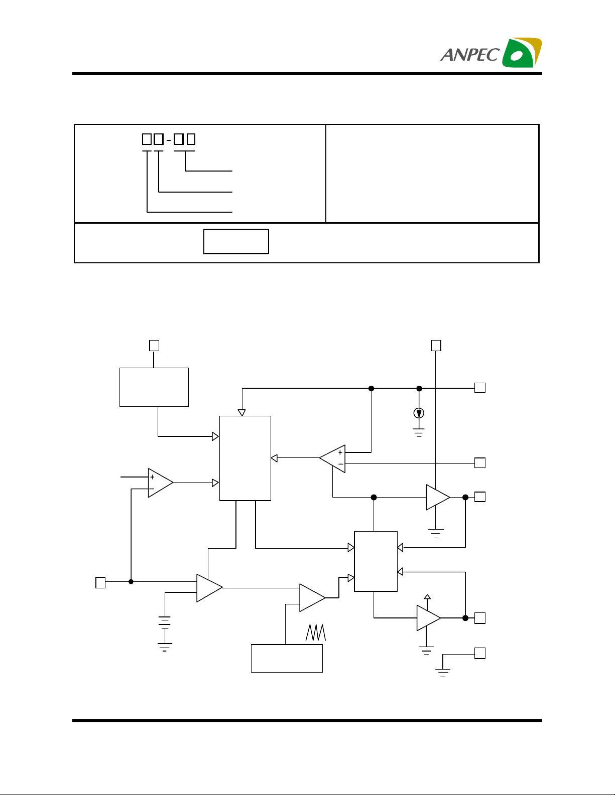
Block Diagram
VCC
UnderVoltage
Lockout
UVLO
0.5V UVP
Handling Code
Temp. Range
Package Code
APW 7057
XXXXX
Soft-Start
and Fault
Logic
Shutdown
OCP
Package Code
K : SO P -8
Operating Junction Tem p. Range
°
C : 0 to 70 C
Handling Code
TU : Tu b e
TR : Tape & Reel
XXXXX - Date Code
OC
Comparator
I
OCSET
40uA
BOOT
OCSET
PHASE
Soft-Start
FB
-
+
Error
REF
V
0.8V
Copyright ANPEC Electronics Corp.
Rev. A.3 - Oct., 2003
Amp lif ier
Inhibit
PW M
COMP
+
-
Oscillator
.ECKH/Figure 1.
OSC
F
300kHz
UGATE
Gate
Control
VCC
LGATE
GND
www.anpec.com.tw2
Page 3
APW7057
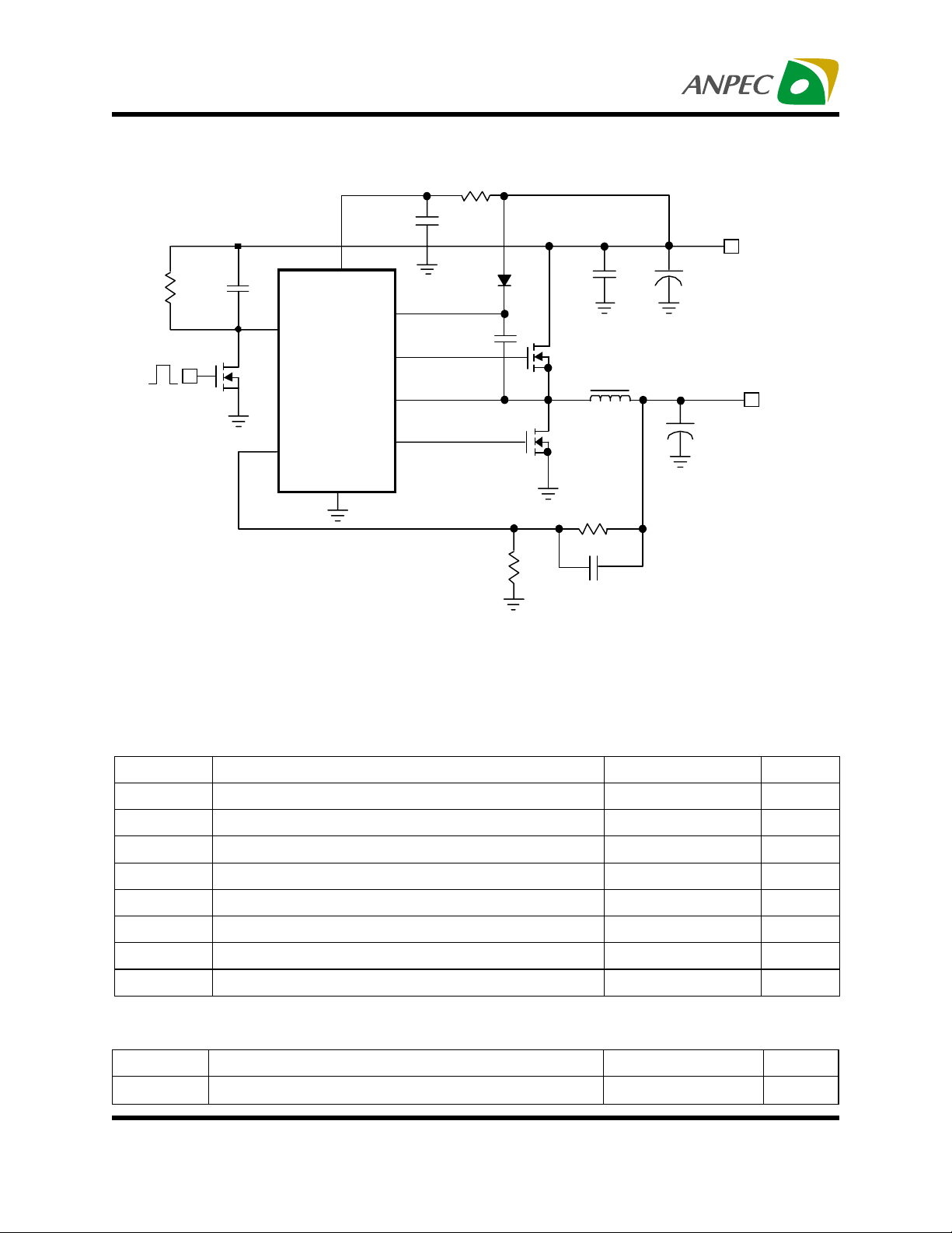
Typical Application
R3
R4
8.2k
C7
470pF
Q3
Shutdown
Q1: APM2014N U C
Q2: APM2014N U C
Q3: APM2300A A C
7
6
OCSET
APW 7057
FB
C3
1uF
5
VCC
BOOT
UGATE
PHASE
U1
LGATE
GND
3
C2: 1000uF/10V, ESR = 25m
C5: 1000uF/6.3V, ESR = 25m
1
2
8
4
1N4148
.ECKH/Figure 2.
2.2
D1
C4
0.1uF
R2
2.4k
V
IN
+
C2
1000uF x2
Q1
L1
3.3uH
C1
1uF
+
Q2
R1
5.1k
C6
0.1uF
Ω
Ω
+5V
C5
1000uF x2
V
OUT
+2.5V/10A
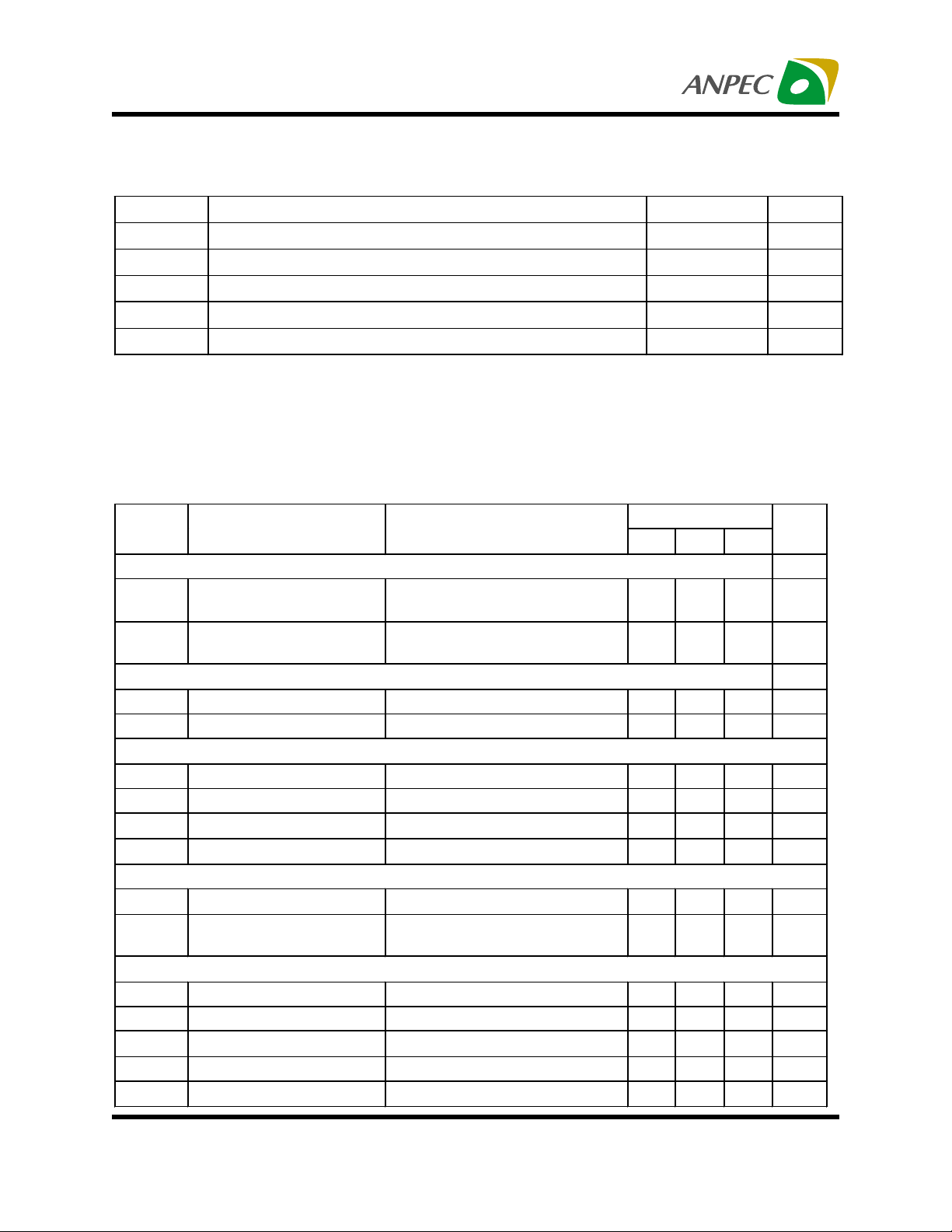
Absolute Maximum Ratings
Symbol Parameter Rating Unit
CC
V
V
BOOT
VCC Supply Voltage (VCC to GND) -0.3 ~ 7 V
BOO T S upply Voltage (BOOT to GN D ) -0.3 ~ 15 V
PHAS E , OC S ET to GND Input Voltage -0.3 ~ 12 V
FB to GN D In p u t Volta ge -0.3 ~ VCC+0.3 V
Maximum Junction Tem perature 125
STG
T
SDR
T
ESD
V
Storage Temperature -65 ~ 150
Maximum Soldering Temperature, 10 Seconds 300
Minim um ESD Rating
±2
Thermal Characteristics
Symbol Parameter Value Unit
JA
θ
Copyright ANPEC Electronics Corp.
Rev. A.3 - Oct., 2003
Junction-to-Ambient Resistance in fre e air (S OP-8) 160
www.anpec.com.tw3
o
o
o
kV
o
C/W
C
C
C
Page 4
APW7057
Recommended Operating Conditions
Symbol Parameter Range Unit
VCC VCC S upply Voltage 5 ± 5% V
V
Output Voltage of the Switc hing Regulator (Note) 0.8 ~ VCC V
OUT
VIN Input Voltage of the S wit c hing Regulat or (Note) 3.3 ~ VCC V
o
C
oC
Unit
P-P
A
µ
TA Am bient Temperature 0 ~ 70
TJ Junction Temperature 0 ~ 125
Note : Refer to the typical application circuit
Electrical Characteristics
Unless otherwise specified, these specifications apply over VCC=5V, VBOOT=12V and TA= 0~70 oC. Typical
values are at TA=25oC.
Symbol Parameter Test Conditions
SUPP LY CURRENT
I
VCC
I
BOOT
VCC No mina l Supp l y
Current
BOOT Nominal Supply
Current
UGATE and LGATE Open
UGATE Open
Under Voltage Lockout(UVLO)
Risi ng V CC Threshold 4.0 4.2 4.4 V
Falli ng V CC Threshold 3.8 4.0 4.2 V
OSCILLATOR
F
Free Running Frequency 250 300 340 kHz
OSC
Ramp Upper Threshol d 2.85 V
Ramp Lower Threshol d 0.95 V
Ramp Amplitude 1.9 V
V
OSC
∆
REFERENCE VOLTAGE
V
Reference Voltage 0.8 V
REF
Referenc e Volt age
Accuracy
-1.5 +1.5 %
ERROR AMPLIFI ER
DC Gain 75 dB
FP Fi rst P ol e F requenc y 10 Hz
FZ Fi rst Zero Frequency 1 kHz
UGATE Dut y Range 0 100 %
FB Input Current
Copyright ANPEC Electronics Corp.
Rev. A.3 - Oct., 2003
APW7057
Min Typ Max
2.1 mA
2.1 mA
0.1
www.anpec.com.tw4
Page 5
APW7057
Electrical Characteristics (Cont.)
Unless otherwise specified, these specifications apply over VCC=5V, VBOOT=12V and TA= 0~70 oC. Typical
values are at TA=25oC.
Symbol Parameter Test Conditions
PWM CONTROLLER GATE DRIVERS
UGATE Source V
UGATE Sink V
LGATE Source
LGATE Sink V
D
T
Dead Time 50 nS
UAGTE
=1V 0.6 A
UGATE
=1V 7 .3
LGATE
=1V 0.6 A
V
LGATE
=1V 1.8
PROTECTIO N
OCSET
I
UV
OCSET Sink Current V
FB
FB Under-Voltage Level FB falling 0.5 V
FB Under-Voltage
Hysteresis
OCSET
=4.5V 34 40 46
15 mV
SOFT-START AND SHUTDOWN
SS
T
Soft-Start Interval 2 mS
Shutdown Threshold V
OCSET Shutdown
Hysteresis
OCSET
Falling 1.25 V
20 mV
APW7057
Unit
Min Typ Max
Ω
Ω
µA
Functional Pin Description
BOOT (Pin 1)
This pin provides the supply voltage to the high side
MOSFET driver. A voltage no greater than 13V can
be connected to this pin as a supply to the driver.
For driving logic level N-channel MOSEFT, a bootstrap circuit can be use to create a suitable driver’s
supply.
UGATE (Pin 2)
This pin provides gate drive for the high-side
MOSFET.
GND (Pin 3)
Signal and power ground for the IC. All voltage levels are measured with respect to this pin. Tie this
pin to the ground plane through the lowest impedance connection available.
Copyright ANPEC Electronics Corp.
Rev. A.3 - Oct., 2003
LGATE (Pin 4)
This pin provides the gate drive signal for the low
side MOSFET.
VCC (Pin 5)
This is the main bias supply for the controller and
its low side MOSFET driver. Must be closely
decoupled to GND (Pin 3). DO NOT apply a
voltage greater than 5.5V to this pin.
FB (Pin 6)
This pin is the inverting input of the error amplifier
and it receives the feedback voltage from an exter-
www.anpec.com.tw5
Page 6

APW7057
Functional Pin Description
nal resistive divider across the output (V
OUT
). The
output voltage is determined by:
VOUT = 0.8V(1+ )
ROUT
RGND
where ROUT is the resistor connected between VOUT
and FB while RGND is the resistor connected from FB
to GND.
OCSET (Pin 7)
This pin serves two functions: as a shutdown control and for setting the over current limit threshold.
Pulling this pin below 1.25V shuts the controller
down, forcing the UGATE and LGATE signals to be
at 0V. A soft start cycle will be initiated upon the release of this pin.
A resistor (R
) connected between this pin and
ocset
the drain of the high side MOSFET will determine
the over current limit. An internally generated 40uA
current source will flow through this resistor, creating a voltage drop. This voltage will be compared
with the voltage across the high side MOSFET. The
threshold of the over current limit is therefore given
by:
40uA x ROCSET
IOI =
RDS(ON)
An over current condition will cycle the soft start
function. After three consecutive cycles and if the
fault condition persists, the controller will be shut
down. To restart the controller, either recycle the V
CC
supply or momentarily pull the OSCSET pin below
1.25V.
PHASE (Pin 8)
This pin is connected to the source of the high-side
MOSFET and is used to monitor the voltage drop
across the high-side MOSFET for over-current
protection.
Typical Characteristics
Reference Voltage vs. Junction Temperature
0.812
0.808
0.804
0.800
0.796
0.792
Reference Voltage, VREF (V)
0.788
-50 - 25 0 25 50 75 100 125 150
Junction Temperature (oC)
Copyright ANPEC Electronics Corp.
Rev. A.3 - Oct., 2003
Switching Frequency vs. Junction Temperature
350
340
330
320
310
300
290
280
270
260
Switching Frequency, FOSC (kHz)
250
-50 -25 0 25 50 75 100 125 150
Junction Temperature (°C)
www.anpec.com.tw6
Page 7

APW7057
Typical Characteristics (Cont.)
OCSET Current vs. Junction T emperature
46
45
44
43
42
41
40
39
38
37
36
OCSET Current , IOCSET (µA)
35
34
-50 -25 0 25 50 75 100 125 150
Junction Temperature (oC)
Operating Waveforms (Refer to the typical application circuit)
1. Load Transient Response : IOUT = 0A -> 10A -> 0A
- IOUT slew rate = Ó 10A/µS
IOUT = 0A -> 10A
Ch1 : VOUT, 100mV/Div, DC,
Offset = 2.50V
Ch2 : VUGATE, 10V/Div, DC
Ax1 : IOUT, 5A/Div
Time : 10µS/Div
BW = 20MHz
V
V
I
OUT
UGATE
OUT
IOUT = 0A -> 10A -> 0A
0A
Ch1 : VOUT, 100mV/Div, DC,
Offset = 2.50V
Ax1 : IOUT, 5A/Div
Time : 100µS/Div
BW = 20MHz
10A
V
OUT
I
OUT
Ch1 : VOUT, 100mV/Div, DC,
Offset = 2.50V
Ch2 : VUGATE, 10V/Div, DC
Ax1 : IOUT, 5A/Div
Time : 10µS/Div
BW = 20MHz
IOUT = 10A -> 0A
V
V
I
OUT
OUT
UGATE
Copyright ANPEC Electronics Corp.
Rev. A.3 - Oct., 2003
www.anpec.com.tw7
Page 8

APW7057
Operating Waveforms (Refer to the typical application circuit)
2. UGATE and LGATE
UGATE Rising
I
=10A
OUT
V
LGATE
Ch1 : VUGATE, 2V/Div, DC Ch2 : VLGATE, 2V/Div, DC
Time : 125nS/Div BW = 500MHz
3. Powering ON / OFF
Soft-start at Powering ON
UGATE Falling
I
=10A
OUT
V
UGATE
V
UGATE
V
LGATE
Ch1 : VUGATE, 2V/Div, DC Ch2 : VLGATE, 2V/Div, DC
Time : 125nS/Div BW = 500MHz
Powering OFF
V
IN
V
IN
Ch1 : VIN, 2V/Div, DC Ch2 : VOUT, 1V/Div, DC
Time : 1mS/Div BW = 20MHz
4. Short-Circuit Protection
UVP
OCP
OCP
V
OUT
I
OUT
V
OUT
V
OUT
Ch1 : VIN, 2V/Div, DC Ch2 : VOUT, 1V/Div, DC
Time : 5mS/Div BW = 20MHz
Under-Voltage (UVP)
and Over-Current Protection (OCP)
Ch1 : VOUT, 1V/Div, DC
Ax1 : IOUT, 10A/Div
Time : 1mS/Div
BW = 20MHz
Copyright ANPEC Electronics Corp.
Rev. A.3 - Oct., 2003
www.anpec.com.tw8
Page 9

APW7057
Application Information
Component Selection Guidelines
Output Capacitor Selection
The selection of C
effective series resistance (ESR) and voltage rating
rather than the actual capacitance requirement. Therefore select high performance low ESR capacitors that
are intended for switching regulator applications. In
some applications, multiple capacitors have to be
paralled to achieve the desired ESR value. If tantalum
capacitors are used, make sure they are surge tested
by the manufactures. If in doubt, consult the capacitors manufacturer.
Input Capacitor Selection
The input capacitor is chosen based on the voltage
rating and the RMS current rating. For reliable
operation, select the capacitor voltage rating to be at
least 1.3 times higher than the maximum input voltage.
The maximum RMS current rating requirement is approximately I
OUT
During power up, the input capacitors have to handle
large amount of surge current. If tantalum capacitors
are used, make sure they are surge tested by the
manufactures. If in doubt, consult the capacitors
manufacturer.
For high frequency decoupling, a ceramic capacitor
between 0.1uF to 1uF can be connected between V
and ground pin.
is determined by the required
OUT
/2 , where I
is the load current.
OUT
CC
∆V
OUT
= I
RIPPLE
x ESR
where Fs is the switching frequency of the regulator.
There is a tradeoff exists between the inductor’s ripple
current and the regulator load transient response time
A smaller inductor will give the regulator a faster load
transient response at the expense of higher ripple current and vice versa. The maximum ripple current occurs at the maximum input voltage. A good starting
point is to choose the ripple current to be approximately 30% of the maximum output current.
Once the inductance value has been chosen, select
an inductor that is capable of carrying the required
peak current without going into saturation. In some
type of inductors, especially core that is make of
ferrite, the ripple current will increase abruptly when it
saturates. This will result in a larger output ripple
voltage.
MOSFET Selection
The selection of the N-channel power MOSFETs are
determined by the R
(C
) and maximum output current requirement.The
RSS
, reverse transfer capacitance
DS(ON)
losses in the MOSFETs have two components: conduction loss and transition loss. For the upper and
lower MOSFET, the losses are approximately given
by the following :
Inductor Selection
P
UPPER
= I
out
2
(1+ TC)(R
DS(ON)
)D + (0.5)(I
)(VIN)(tsw)F
out
The inductance of the inductor is determined by the
output voltage requirement. The larger the inductance,
P
LOWER
2
= I
(1+ TC)(R
out
DS(ON)
)(1-D)
the lower the inductor’s current ripple. This will translate into lower output ripple voltage. The ripple current
and ripple voltage can be approximated by:
.E
I
VIN - V
=
RIPPLE
Copyright ANPEC Electronics Corp.
Rev. A.3 - Oct., 2003
Fs x L
OUT
V
OUT
x
V
IN
where I
is the load current
OUT
TC is the temperature dependency of R
FS is the switching frequency
t
is the switching interval
sw
D is the duty cycle
www.anpec.com.tw9
S
DS(ON)
Page 10

APW7057
Application Information
Note that both MOSFET s have conduction losses while
the upper MOSFET include an additional transition
loss.The switching internal, t
reverse transfer capacitance C
, is a function of the
sw
. Figure 3 illustrates
RSS
the switching waveform internal of the MOSFET.
The (1+TC) term is to factor in the temperature dependency of the R
“R
vs T emperature” curve of the power MOSFET.
DS(ON)
and can be extracted from the
DS(ON)
Layout Considerations
In high power switching regulator, a correct layout is
important to ensure proper operation of the regulator.
In general, interconnecting impedances should be minimized by using short, wide printed circuit traces. Signal and power grounds are to be kept separate and
finally combined using ground plane construction or
V
DS
single point grounding. Figure 4 illustrates the layout,
with bold lines indicating high current paths. Components along the bold lines should be placed close
together. Below is a checklist for your layout:
• •
• Keep the switching nodes (UGA TE, LGATE and
• •
PHASE) away from sensitive small signal nodes
since these nodes are fast moving signals. There
fore keep traces to these nodes as short as
possible.
••
• Decoupling capacitor C
••
provides the bulk capaci
IN
tance and needs to be placed close to the IC since
it will provide the MOSFET drivers transient current
requirement.
• •
• The ground return of C
• •
C
••
• Capacitor C
••
(-) terminal.
OUT
should be connected as close to
BOOT
must return to the combine
IN
the BOOT and PHASE pins as possible.
V
C
HF
IN
Voltage across
drain and source of MOS FET
t
sw
Figure 3. Switching waveform across M O SFET
Copyright ANPEC Electronics Corp.
Rev. A.3 - Oct., 2003
Time
C
+
Q1
IN
Q2
www.anpec.com.tw10
5
VCC
BOOT
LGATE
APW7057
U
UGATE
1
PHASE
Figure 4. Reco mmended Layout Diagram
1
4
2
8
L1
C
OUT
+
V
OUT
Page 11

APW7057
Packaging Information
SOP-8 pin ( Reference JEDEC Registration MS-012)
HE
0.015X45
e1 e2
D
A1
A
1
L
0.004max.
Dim
A 1.35 1.75 0.053 0.069
A1 0.10 0.25 0.004 0. 010
D 4.80 5.00 0.189 0.197
E 3.80 4.00 0.150 0.157
H 5.80 6.20 0.228 0.244
L 0.40 1.27 0.016 0.050
e1 0.33 0.51 0.013 0.020
e2 1.27BSC 0.50BSC
18
φ
Millimeters Inches
Min. Max. Min. Max.
°
8
°
Copyright ANPEC Electronics Corp.
Rev. A.3 - Oct., 2003
www.anpec.com.tw11
Page 12

APW7057
Physical Specifications
Terminal Material Solder-Plated Copper (Solder Material : 90/10 or 63/37 SnPb
Lead Solderability Meets EIA Specification RSI86-91, ANSI/J-STD-002 Category 3.
Packaging 2500 devices per reel
Reflow Condition (IR/Convection or VPR Reflow)
Reference JEDEC Standard J-STD-020A APRIL 1999
Peak temperature
temperature
Pre-heat temperature
°
183 C
Time
Classification Reflow Profiles
Convection or IR/
Convection
Average ramp-up rate(183°C to Peak) 3°C/second max. 10°C /second max.
Preheat temperature 125± 25°C)
°
Temperature maintained above 183
Time within 5°C of actual peak temperature
Peak temperature range
Ramp-down rate
Time 25°C to peak temperature
C
120 seconds max.
60 ~ 150 seconds
10 ~ 20 seconds
°
220 +5/-0
°
C /second max. 10°C /second max.
6
6 minutes max.
C or 235 +5/-0°C 215~ 219°C or 235 +5/-0°C
60 seconds
VPR
Package Reflow Conditions
pkg. thickness
and all bags
Convection 220 +5/-0°C
VPR 215-219°C
IR/Convection 220 +5/-0
Copyright ANPEC Electronics Corp.
Rev. A.3 - Oct., 2003
2.5mm
≥≥≥≥
°
C IR/Convection 235 +5/-0
pkg. thickness < 2.5mm and
pkg. volume
≥≥≥≥
350 mm
pkg. thickness < 2.5mm and pkg.
volume <
°
Convection 235 +5/-0
VPR 235 +5/-0
°
C
C
°
C
www.anpec.com.tw12
Page 13

APW7057
Re lia bility test p r o gram
Test item Method Description
SOLDERABILITY MIL-STD-883D-2003
HOLT MIL-STD-883D-1005.7
PCT JESD-22-B, A102
TST MIL-STD-883D-1011.9
ESD MIL-STD-883D-3015.7 VHBM > 2KV, VMM > 200V
Latch-Up JESD 78 10ms , Itr > 100mA
Carrier Tape & Reel Dimension
245°C , 5 SEC
1000 Hrs Bias @ 125 °C
168 Hrs, 100 % RH , 121°C
-65°C ~ 150°C, 200 Cycles
t
W
E
F
Po
A
P
P1
Ao
J
D
Bo
D1
C
Ko
T2
B
T1
Application
SOP-8
A B C J T1 T2 W P E
330±162 ± 1.5
F D D1 Po P1 Ao Bo Ko t
5.5 ± 0.1 1.55±0.1
12.75 +
0.1 5
1.55+ 0.25
2 + 0.5 12.4 +0.2
4.0 ± 0.1 2.0 ± 0.1 6.4 ± 0.1 5.2± 0.1 2.1± 0.1 0.3±0.013
2± 0.2
12 + 0.3
- 0.1
8± 0.1 1.75± 0.1
(mm)
Copyright ANPEC Electronics Corp.
Rev. A.3 - Oct., 2003
www.anpec.com.tw13
Page 14

APW7057
Cover Tape Dimensions
Application Carrier Width Cover Tape Width Devices Per Reel
SOP- 8
Customer Service
Anpec Electronics Corp.
Head Office :
5F, No. 2 Li-Hsin Road, SBIP,
Hsin-Chu, T aiwan, R.O.C.
T el : 886-3-5642000
Fax : 886-3-5642050
Taipei Branch :
7F, No. 137, Lane 235, Pac Chiao Rd.,
Hsin Tien City, Taipei Hsien, Taiwan, R. O. C.
T el : 886-2-89191368
Fax : 886-2-89191369
12 9.3 2500
Copyright ANPEC Electronics Corp.
Rev. A.3 - Oct., 2003
www.anpec.com.tw14
 Loading...