

Datasheet APW7055D-NC-TU, APW7055D-NC-TR, APW7055C-NC-TU, APW7055C-NC-TR, APW7055B-NC-TU Datasheet (ANPEC)
...Page 1
Copyright ANPEC Electronics Corp.
Rev.A.1 - Dec., 2001
APW7055
www.anpec.com.tw1
ANPEC reserves the right to make changes to improve reliability or manufacturability without notice, and advise
customers to obtain the latest version of relevant information to verify before placing orders.
Features
••
••
•
Operates from 5V input supply
••
••
•
2 Regulated Voltage are provided
− Standard Buck Switching Power for VMEM
(2.5V)
− Linear Controller with Source-Sink Regula
tion for VTT(1.25V)
••
••
• Simple Single-Loop Control Design
− Voltage-Mode PWM Control
••
••
• Excellent Output Voltage Regulation
− VMEM Output : V
MEM
±1.5% Over Tem-per
ature
− VTT Output : 1/2 VIN ±25mV Over Tempera-
ture
••
••
• Fast Transient Response
− Built-in Feedback Compensation
− Full 0% to 100% Duty Ratio
••
••
• Over-Voltage and Over-Current Fault Monitors
••
••
• Constant Frequency Operation(200kHz)
• •
• •
• 16 pins, SSOP Package
Applications
••
••
• M/B DDR Power Regulation
••
••
• AGP/PCI Graphics Power Regulation
••
••
• SSTL-2 Termination
General Description
The APW7055 provides the power control and protec-
tions for two output voltages on M/B DDR applications.
It integrates one PWM controller , one source-sink
linear controller(LC) for DDR source-sink purpose, as
well as the monitor and protection functions into a
single package. The PWM controller supplies the
VMEM(2.5V) with a standard buck converter. The
source-sink linear controller regulates VTT(1.25V)
power for DDR Termination.
Additional built-in over-voltage protection (OVP) will
be started when the VMEM output is above 115% of
the internal DAC setting(V
DAC
) . OVP function will shut-
down the upper MOSFET and disable all output volt-
age . The PWM controllers over-current function moni-
tors the output current by sensing the voltage drop
across the upper MOSFETs r
DS(ON)
, eliminating the
need for a current sensing resistor .
Advanced PWM and Linear Power Controller
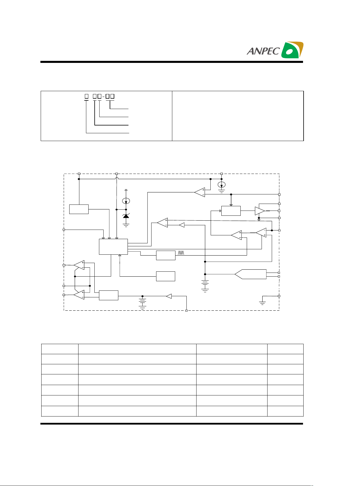
Pin Description
SINK
PHASE
MEM1
PGND
BOOT
UGATE
SS
VCC
GND
MEM0
OCSET
VSEN
11
10
12
9
13
16
8
14
15
7
6
5
4
3
SOURCE
FB
VIN
SD
1
2
Page 2
Copyright ANPEC Electronics Corp. Rev. A.
Rev.A.1 - Dec., 2001
)29%##
www.anpec.com.tw2
Ordering Information
Block Diagram
APW7055
Voltage Code
A : 2.40~2.55V B : 2.60~2.75 V
C : 2.80~2.95V D : 3.00~3.15 V
Package Code
N : S SO P-1 6
Tem p. R ang e
C : 0 to 70
°
C
Handling Code
TU : Tub e T R : Tape & Re el
Handling Code
Tem p. R ang e
Package Code
Voltage Code
Absolute Maximum Ratings
Symbol Parameter Rating Unit
V
CC
Supply Voltage 15 V
VI , V
O
Input , Output or I/O Voltage GND -0.3 V to VCC +0.3 V
T
A
Operating Ambient Temperature Range 0 to 70
°
C
T
J
Junction Temperature Range 0 to 125
°
C
T
STG
Storage Temperature Range -65 to +150
°
C
T
S
Soldering Temperature 300 ,10 seconds
°
C
VCC
Power On
Reset
Therm al
Protection
V
TT
Control
So ft Sta rt and
Fa ult Lo gic
O sc illator
Gate
Control
TT L D /A
Converter
SD
SOURCE
FB
SINK
VCC SS OCSET
BOOT
PGND
VSEN
MEM0
MEM1
GND
28
µ
A
4.5V
IN H IBIT
PWM
OCP
OVP
115%
PHASE
UGATE
V
MEM
200uA
E.A
50%
V
TT
V
IN
Page 3
Copyright ANPEC Electronics Corp. Rev. A.
Rev.A.1 - Dec., 2001
)29%##
www.anpec.com.tw3
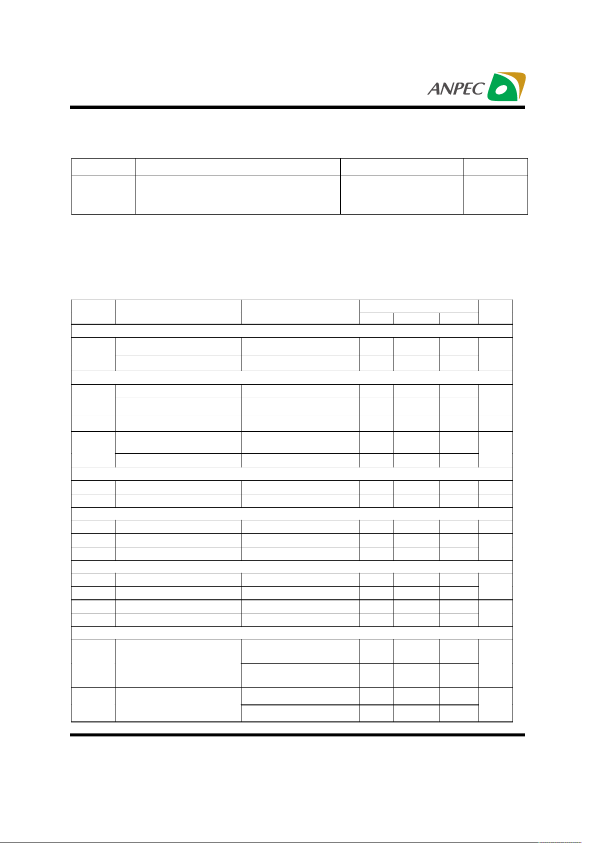
Electrical Characteristics
Thermal Characteristics
Symbol Parameter Value Unit
R
JA
Thermal Resistance in Free Air
SOIC
SOIC (with 3in
2
of Copper)
75
65
°
C/W
1. Recommended operating conditions, Unless otherwise noted.
2. Refer to Block and Simplified Power System Diagrams , and Typical Application Schematic.
APW7055
Symbol Parameter Test Conditions
Min. Typ. Max.
Unit
Supply Current
Nominal Supply Current SD=0V, GATE Drive Open 7
I
CC
Shutdown Supply Current SD=5V 2.7
mA
Power-on Reset
Rising VCC Threshold Vocset=3V 4.2 4.6
V
CC
Falling VCC Threshold Vocset=3V 3.6
V
V
OCSET
Rising V
OCSET
Threshold 1.26 V
Shutdown Input High
Voltage
2.0
V
SD
Shutdown Input Low Voltage 0.8
V
Oscillator
F
OSC
Free Running Frequency 185 200 215 kHz
∆
V
OSC
Ramp Amplitude 1.9 V
PWM Controller Reference Voltage
V
DAC
DAC Voltage Accuracy -1.5 +1.5 %
MEM0-1 Input High Voltage 2.0
MEM0-1 Input Low Voltage 0.8
V
Source-Sink Linear Controller
V
SOURCE
Source Regulation Voltage -10mV 0.495VIN +10mV
V
SINK
Sink Regulation Voltage -10mV 0.505VIN +10mV
V
I
Source
Source Drive Current 0.8
I
SINK
Sink Drive Current 0.8
mA
PWM Controllers Gate Drivers
VCC=5V,V
BOOT
=9.5V,
V
UGATE
=6V
1
I
UGATE
UGATE Source
V
CC
=12V,V
BOOT
=9.5V,
V
UGATE
=6V
1
A
VCC=5V,V
UGATE
=1V 3
R
GATE
UGATE Sink
VCC=12V, V
UGATE
=6V 3 3.5
Ω
Page 4
Copyright ANPEC Electronics Corp. Rev. A.
Rev.A.1 - Dec., 2001
)29%##
www.anpec.com.tw4
Functional Pin Description
VCC (Pin 1)
Provide a +5V bias supply for the IC to this pin. This
pin also provides the gate bias charge for the MOS
FETs of the source-sink regulator. The voltage at th
is pin is monitored for Power-On Reset (POR)
purposes.
SS (Pin 2)
This pin provides the soft start for the standard buck
converter and source-sink regulator. Connect a ca-
pacitor from this pin to ground.This capacitor, along
with an internal 28uA current source,sets the soft-start
interval of the converter and preventing the outputs from
overshoot as well as limiting the input current .
SD (Pin 3)
The pin shuts down all the outputs. A TTL-compatible,
logic level high signal applied at this pin immediately
discharges the soft-start capacitor,disabling all the
outputs.When IC re-enabled, the IC undergoes a new
soft-start cycle.Left open, this pin is pulled low by an
internal pull-down resistor,enabling operation.
SOURCE (Pin 4)
Connect the pin to the upper MOSFET gate drive of
the source-sink regulator. This pin is used to drive the
1. Recommended operating conditions, Unless otherwise noted.
2. Refer to Block and Simplified Power System Diagrams , and Typical Application Schematic.
APW7055
Symbol Parameter Test Conditions
Min. Typ. Max.
Unit
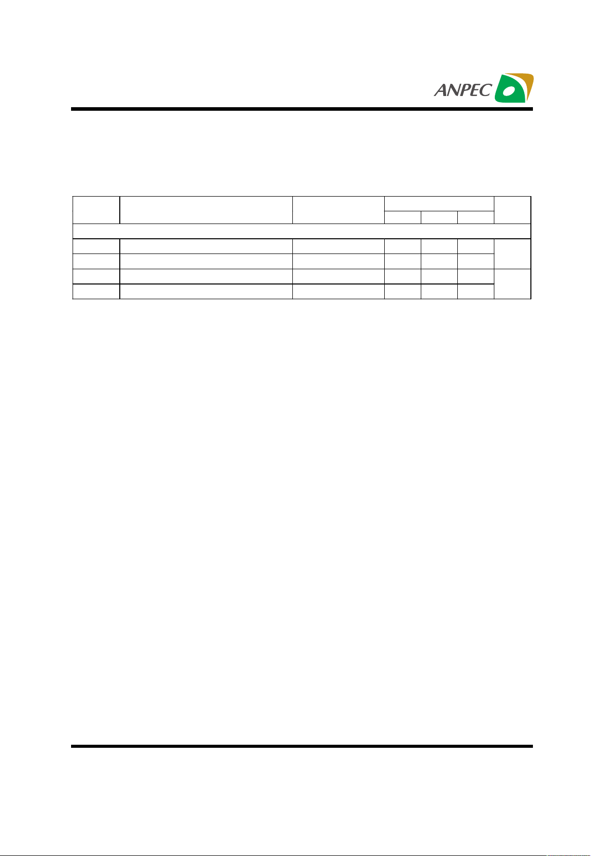
Protection
VSEN O.V. trip point (VSEN/V
DAC
) VSEN Rising 115 120
VSEN O.V. Hysteresis 2
%
I
OCSET
Ocset Current Source Vocset=3V 170 200 230
I
SS
Soft start Current 28
uA
upper external MOSFET as a source regulator.
SINK (Pin 5)
Connect the pin to the lower MOSFET gate drive of
the source-sink regulator.This pin is used to drive the
lower external MOSFET as a sink regulator.
FB (Pin 6)
Connect this pin to output of the source-sink regulator.
This pin provide the voltage feedback path for source
and sink regulators. This pin is internally connected
to the negative input of the source controller, and also
connected to the positive input of the sink controller.
VIN (Pin 7)
Connect this pin to a voltage source. Two voltages,
above 0.5VIN, are generated by an internal resistor
divider as the reference voltage of the source and sink
controllers. The internal resistor divider provides an
offset voltage to ensure higher sink regulation voltage
and prevent an direct current path through the upper
and lower MOSFETs, damaging the two MOSFETs.
GND (Pin 8)
Signal ground for the IC. All voltage levels are mea
sured with respect to this pin voltage protection.
Electrical Characteristics (Cont.)
Page 5

Copyright ANPEC Electronics Corp. Rev. A.
Rev.A.1 - Dec., 2001
)29%##
www.anpec.com.tw5
Functional Pin Description (Cont.)
VSEN (Pin 9)
This pin is connected to the standard buck converters
output voltage to provide the voltage feedback path for
PWM converter. The OVP(Over-Voltage-Protection)
comparator circuit use this signal to monitor output
voltage status for over-voltage protection.
OCSET (Pin 10)
Connect a resistor (R
OCSET
) from this pin to the drain of
the standard buck PWM converters MOSFET. R
OCSET
,
an internal 200mA current source (I
OCSET
), and the
MOSFETs on-resistance(r
DS(ON)
) set the converters
over-current (OC) trip point according to the following
equation:
I
PEAK
=
I
OCSET
x R
OCS ET
r
DS(ON)
An over-current trip cycles the soft-start function
.
MEM0-1 (Pin 11-12)
MEM0-1 are TTL-compatible logic level input pins of
the 2-bits DAC.The status of these 2 pins set the in-
ternal reference voltage(V
DAC
) for the standard buck
converter and also sets the OVP threshold voltage.Table
1 shows the DAC table voltage.
PGND (Pin 13)
This is the power ground connection.Tie this pin to
the anode of the flywheel diode of the standard buck
PWM converters circuit.
PHASE (Pin 14)
Connect the PHASE pin to the standard buck PWM
converters MOSFET source.This pin is used to moni-
tor the voltage drop across the MOSFET for over-cur
rent protection.
UGATE (Pin 15)
Connect this pin to the MOSFET gate of the standard
buck PWM converter.This pin provides the gate drive
for the external MOSFET.
BOOT (Pin 16)
This pin provides bias voltage to the external MOSFET
driver. A bootstrap circuit may be used to pump a
boot voltage for enforcing the driving capability of the
gate driver and improving the performance of the
MOSFET.
Table 1 DAC Table
APW7055 - A APW7055 - B
Pin Name
MEM1 MEM0
V
MEM
Voltag e
0 0 2.60
0 1 2.65
1 0 2.70
1 1 2.75
Pin Name
MEM1 MEM0
V
MEM
Voltag e
0 0 2.40
0 1 2.45
1 0 2.50
1 1 2.55
Page 6

Copyright ANPEC Electronics Corp. Rev. A.
Rev.A.1 - Dec., 2001
)29%##
www.anpec.com.tw6
Simplified Power System Diagram
Table 1 DAC Table
APW7055 - C APW7055 - D
Pin Name
MEM1 MEM0
V
MEM
Voltag e
0 0 3.00
0 1 3.05
1 0 3.10
1 1 3.15
Pin Name
MEM1 MEM0
V
MEM
Voltag e
0 0 2.80
0 1 2.85
1 0 2.90
1 1 2.95
Source-Sink
LC
APW 7055
PWM
Controller
V
MEM
Q1
5VDUAL
V
MEM
Q3
V
66
Q2
D1
Page 7

Copyright ANPEC Electronics Corp. Rev. A.
Rev.A.1 - Dec., 2001
)29%##
www.anpec.com.tw7
Typical Application Circuit
OCSET
10
UGATE
15
PHASE
14
BOOT
16
PGND
13
VSEN
9
MEM0
11
SS
2
MEM1
12
SD
3
SINK
5
SOURCE
4
FB
6
VCC
1
GND
8
VIN
7
U1
)29%##
R2
1k
+
C4
1000 uF
R5
0
R6
SPARE
C1
1uF
C1 0
1uF
1
2
4
3
J2
C1 1
0.1uF
R3
0
R7
0
R8
NC
+
C1 2
1000 uF
VTT
VMEM
Q1
APM9410
Q2A
APM7313
D1
B3 4
+
C5
1000 uF
+
C3
1000 uF
C6
200p F
+
C7
1000 uF
VMEM
Q2B
APM7313
R1
10
+5VDUAL
C1 3
0.1uF
R4
10k
C1 4
0.1uF
+
C8
1000 uF
+
C1 7
1000 uF
R1 1
NC
VIN
D4
1N414 8
5VSB
D5
1N414 8
R1 2
1k
L1
2uH
L2
4.7uH
Page 8

Copyright ANPEC Electronics Corp. Rev. A.
Rev.A.1 - Dec., 2001
)29%##
www.anpec.com.tw8
N
12
3
EH
D
L
GAUGE
PLANE
1
e
B
A1
A
Millimeters Variations- D Inches Variations- D
Dim
Min. Max. Variations Min. Max.
Dim
Min. Max. Variations Min. Max.
A1.350
1.75
SSOP-16
4.75 5.05
A 0.053 0.069 SSOP-16 0.187 0.199
A1
0.10 0.25
A1 0.004 0.010
B
0.20 0.30
B 0.008 0.012
D See variations D See variations
E
3.75 4.05
E 0.147 0.160
e 0.625 TYP. e 0.025 TYP.
H
5.75 6.25
H 0.226 0.246
L
0.4 1.27
L 0.016 0.050
N See variations N See variations
φ
1 0
°
8
°φ
1 0
°
8
°
SSOP-16
Package Informaion
Page 9

Copyright ANPEC Electronics Corp. Rev. A.
Rev.A.1 - Dec., 2001
)29%##
www.anpec.com.tw9
Reference JEDEC Standard J-STD-020A APRIL 1999
Reflow Condition (IR/Convection or VPR Reflow)
Physical Specifications
Pre-heat temperature
183 C
Peak temperature
Time
°
temperature
Terminal Material Solder-Plated Copper (Solder Material : 90/10 or 63/37 SnPb)
Lead Solderability Meets EIA Specification RSI86-91, ANSI/J-STD-002 Category 3.
Packaging 1000 devices per reel for SO-16 , 2500 devices per reel for SSOP-16.
Classification Reflow Profiles
Convection or IR/
Convection
VPR
Average ramp-up rate(183°C to Peak) 3°C/second max. 10 °C /second max.
Preheat temperature 125 ± 25°C)
120 seconds max
Temperature maintained above 183°C
60 150 seconds
Time within 5°C of actual peak temperature
10 20 seconds 60 seconds
Peak temperature range
220 +5/-0°C or 235 +5/-0°C 215-219°C or 235 +5/-0°C
Ramp-down rate
6 °C /second max. 10 °C /second max.
Time 25°C to peak temperature
6 minutes max.
Package Reflow Conditions
pkg. thickness ≥≥≥≥ 2.5mm
and all bgas
pkg. thickness < 2.5mm and
pkg. volume ≥≥≥≥ 350 mm³
pkg. thickness < 2.5mm and pkg.
volume < 350mm³
Convection 220 +5/-0 °C Convection 235 +5/-0 °C
VPR 215-219 °C VPR 235 +5/-0 °C
IR/Convection 220 +5/-0 °C IR/Convection 235 +5/-0 °C
Page 10

Copyright ANPEC Electronics Corp. Rev. A.
Rev.A.1 - Dec., 2001
)29%##
www.anpec.com.tw10
Reliability test program
Test item Method Description
SOLDERABILITY MIL-STD-883D-2003
245°C , 5 SEC
HOLT MIL-STD-883D-1005.7
1000 Hrs Bias @ 125 °C
PCT JESD-22-B, A102
168 Hrs, 100 % RH , 121°C
TST MIL-STD-883D-1011.9
-65°C ~ 150°C, 200 Cycles
ESD MIL-STD-883D-3015.7 VHBM > 2KV, VMM > 200V
Latch-Up JESD 78 10ms , IJH > 100mA
Carrier Tape & Reel Dimensions
t
Ao
E
W
Po
P
Ko
Bo
D1
D
F
P1
A
J
B
T2
T1
C
Application
A B C J T1 T2 W P E
SSOP-16
330±3 100 ± 2
13 + 0.5
2 ± 0.5
16.4 +0.3
-0.2
2.5± 0.5 16 ± 0.2 12± 0.1 1.75± 0.1
Application
F D D1 Po P1 Ao Bo Ko t
SSOP-16 7.5 ± 0.1
1.5 +0.1 1.5 +0.25
4.0 ± 0.1 2.0 ± 0.1 10.9 ± 0.1 10.8± 0.1 3.0± 0.1 0.3±0.013
(mm)
Page 11

Copyright ANPEC Electronics Corp. Rev. A.
Rev.A.1 - Dec., 2001
)29%##
www.anpec.com.tw11
Cover Tape Dimensions
Carrier Width
16 16
Cover Tape Width
13.3 13.3
(mm
)
Anpec Electronics Corp.
Head Office :
5F, No. 2 Li-Hsin Road, SBIP,
Hsin-Chu, Taiwan, R.O.C.
Tel : 886-3-5642000
Fax : 886-3-5642050
Taipei Branch :
7F, No. 137, Lane 235, Pac Chiao Rd.,
Hsin Tien City, Taipei Hsien, Taiwan, R. O. C.
Tel : 886-2-89191368
Fax : 886-2-89191369
Customer Service
 Loading...