

Datasheet APW7037RC-TR, APW7037KC-TU, APW7037KC-TR, APW7037ARC-TU, APW7037ARC-TR Datasheet (ANPEC)
...Page 1
APW7037/A
8-PIN Synchronous Buck PWM Controller
Features
••
•
Operating with Single 5V or 12V Input
••
••
•
Drives N-Channel MOSFETs
••
••
•
Simple Single-Loop Control Design
••
− Voltage-Mode PWM Control
− Full 0% to 100% Duty Ratio
− Fast Transient Response
••
• ±2% Output Voltage Accuracy Over Temperature
••
••
• Under-Voltage Protection for Output
••
••
• 200kHz Constant Frequency Operation
••
(400kHz for APW7037A)
••
• Small size, 8-PIN Package (SOIC or TSSOP)
••
Applications
••
• Graphics Cards
••
••
• DDR Memory Power Supply
••
••
• DDR Memory Termination Voltage
••
General Description
The APW7037/A controller IC is designed to provide
a low cost synchronous Buck regulator for on-board
DC to DC converter applications. The APW7037 to-
gether with dual N-channel MOSFETs such as
APM7313, provide a low cost solution for such
applications. This device features an internal 200KHz
oscillator (400KHz for “A” version), Power-On-Reset
(POR) for both VCC and VC supplies, an external
programmable soft-start function as well as output
under-voltage detection that latches off the device
when an output short is detected.
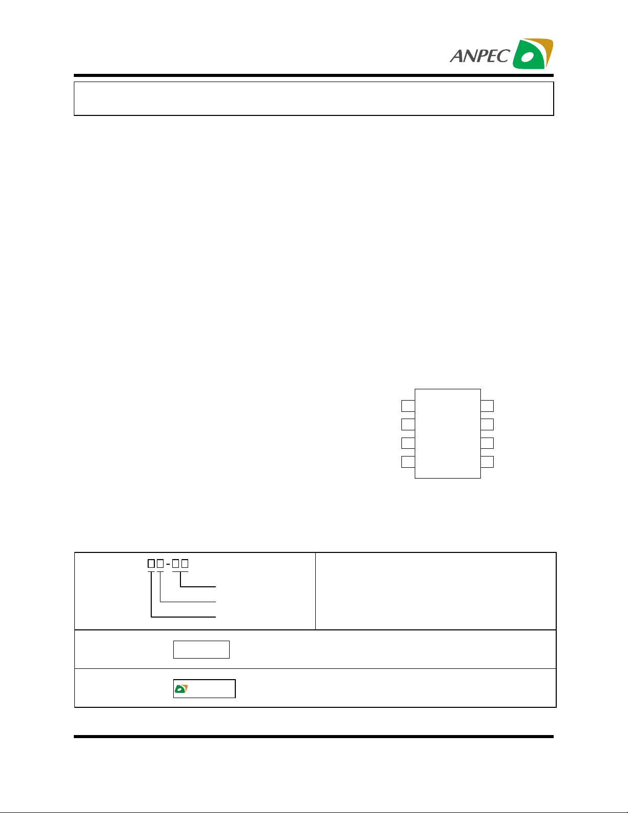
Pin Description
1
VCC
LDRV
GND HDRV
2
3
45
8FB
SS
7
COMP
6
VC
••
• Low-Voltage Distributed Power Supplies
••
Ordering and Marking Information
APW7037/A
Handling Code
Temp. Range
Package Code
APW 7037/A K :
APW 7037/A R :
ANPEC reserves the right to make changes to improve reliability or manufacturability without notice, and advise
customers to obtain the latest version of relevant information to verify before placing orders.
Copyright ANPEC Electronics Corp.
Rev. A.4 - May, 2003
APW 7037/A
XXXXX
APW 7037/A
XXXXX
Package Code
K : S O-8 R : TS SO P-8
Operating Junction Temp. Range
C : 0 to 70°C
Handling Code
TU : Tube
TR : Tape & R eel
XXXXX - Date Code
XXXXX - Date Code
www.anpec.com.tw1
Page 2
APW7037/A
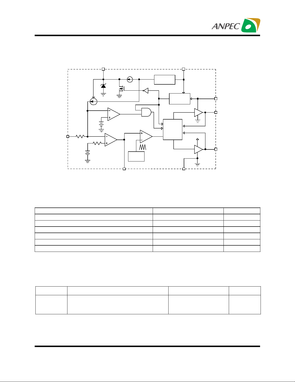
Block Diagram
SS
20uA
3.3V
Max .
64uA
Under-Voltage
V
FBUV
FB
25k
25k
V
REF
Error
Amp.
COMP
OSC
F
OSC
Absolute Maximum Ratings
4.5V
Regulator
PW M
POR
Po w e r
On Reset
Gate
Control
VCC
VC
HDRV
VCC
LDRV
GND
Description Rating Unit
VCC to GND -0.2~30 V
VC to GND -0.2~30 V
Operating Junction Temperature 0~125 °C
Storage Temperature -65~150 °C
Soldering Temperature (10 Seconds) 300 °C
Minimum ESD Rating ±2 kV
Thermal Characteristics
Symbol Parameter Value Unit
θ
JA
Copyright ANPEC Electronics Corp.
Rev. A.4 - May, 2003
Thermal Resistance in Free Air
8-pin SOIC
8-pin TSSOP
160
124
°
www.anpec.com.tw2
C/W
Page 3
APW7037/A
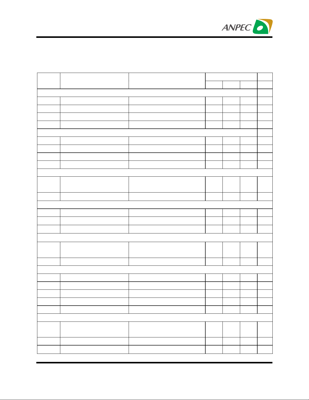
Electrical Characteristics
Unless otherwise specified, these specifications apply over VCC=5V, VC=12V and TA=0 to 70°C. Typical values refer
A=25°C.
to T
APW7037/A Unit
Symbol Parameter Test Conditions
SUPPLY CURRENT
I
I
CCQ
I
VCC Dynamic Supply Current F
CC
I
VC Dynamic Supply Current F
C
VCC Static Supply Current
VC Static Supply Current SS=GND 0.2 0.4 1 mA
CQ
=200KHz, CL=1500pF 2 3 5 mA
OSC
=200KHz, CL=1500pF 2 5.5 8 mA
OSC
SS=GND
POWER-ON RESET
Rising VCC Threshold 4.0 4.2 4.4 V
VCC POR Hysteresis 0.25 V
Rising VC Threshold 3.1 3.3 3.5 V
VC POR Hysteresis 0.2 V
OSCILLATOR
F
V
∆
Free Running Frequency
OSC
Ramp Amplitude
OSC
1.10 V
APW7037
APW7037A
ERROR AMPLIFIER
I
I
FB Pin Input Bias Current SS=3V, VFB=1V
FB1
FB Pin Input Bias Current
FB2
SS=0V, V
FB
=1V
GM Transconductance 450 600 750
REFERENCE VOLTAGE
V
FB Pin Regulation Voltage
FB
APW7037
APW7037A
LREG VFB Line Regulation VCC = 5~12V 0.2 0.35 %
GATE DRIVERS
HDRV Rising Time CL = 1500pF 20 50 nS
HDRV Falling Time CL = 1500pF 15 50 nS
LDRV Rising Time CL = 1500pF 25 50 nS
LDRV Falling Time CL = 1500pF 25 50 nS
Dead Band Time 50 150 250
PROTECTION
V
FB Under-Voltage Threshold VFB Falling APW7037
FBUV
APW7037A
V
Shutdown Threshold Voltage Pull the voltage of SS pin 0.5 V
SD
Soft-Start Current SS=0 10 20 30
I
SS
Min. Typ. Max.
0.5 1.5 3 mA
180
360
200
400
220
440
1nA
-64
µ
1.225
0.784
0.4
0.3
1.250
0.800
0.6
0.4
1.275
0.816
0.8
0.5
KHz
A
µ
mho
V
nS
V
A
µ
Copyright ANPEC Electronics Corp.
Rev. A.4 - May, 2003
www.anpec.com.tw3
Page 4

APW7037/A
Functional Pin Description
FB (Pin 1)
Connect this pin to the output (VOUT) of the PWM con-
verter via an external resistor divider to provide a volt-
age feedback path for the converter. The output volt-
age set by the resistor divider is determined using the
following formula :
OUT
R
()
VOUT = VREF x
1+
GND
R
where ROUT is the resistor connected from VOUT to FB
, and RGND is the resistor connected from FB to ground.
The voltage at this pin is also monitored for Under-
Voltage protection.
VCC (Pin 2)
Connect this pin to input voltage from 5V to 20V. This
pin provides the bias for the control circuitry and the
low-side power MOSFET driver (LDRV). The voltage
at this pin is monitored for Power-On Reset (POR)
purpose.
HDRV (Pin 5)
Connect this pin to the gate of the high-side power
MOSFET. This pin provides the gate drive for the
MOSFET.
VC (Pin 6)
This pin provides bias voltage to the high-side
MOSFET driver. A bootstrap circuit may be used to
pump a boot voltage for enforcing the driving capabil-
ity of the gate driver and improving the performance of
the MOSFET.
COMP (Pin 7)
This pin is the output of the error amplifier. Add an
external resistor-capacitor network to provide a loop
compensation for the PWM converter.
SS (Pin 8)
LDRV (Pin 3)
Connect this pin to the gate of the low-side power
MOSFET. This pin provides the gate drive for the
MOSFET.
GND (Pin 4)
Signal and power ground for the IC. All voltage levels
are measured with respect to this pin.
Copyright ANPEC Electronics Corp.
Rev. A.4 - May, 2003
Connect a capacitor from this pin to ground.This
capacitor, along with an internal 20uA current source,
sets the soft-start interval of the PWM converter and
prevents the outputs from overshoot as well as limits
the input current. Pull this pin below 0.5V can shut-
down the converter.
www.anpec.com.tw4
Page 5

APW7037/A
Typical Applications
1. Dual supply voltage(5V and 12V) application
C1
1uF
2
VCC
Q2
AP M2300A
C7
0.1uF
8
SS
APW7037
Shutdown
7
COM P
R3
24k
C8
2200pF
2. Single supply voltage(5V) application
R4
3
U1
GND
+12V
V
C3
47uF
IN
+5V
V
OUT
VC
HDRV
C2
6
1uF
5
Q1A
AP M7313
C5
1uF
100uF
L4
3.3uH
C4
L3
1uH
1.5V/5 A
LDRV
3
Q1B
APM7313
C6,C9
2 x 150uF
R1
1
FB
4
249
R2
1.24k
C1
1uF
VCC
Q2
APM2300A
8
SS
C8
Shutdown
0.1uF
7
COM P
R3
24k
C9
2200pF
Copyright ANPEC Electronics Corp.
Rev. A.4 - May, 2003
R4
3
D3
1N4148
2
U1
APW7037
GND
D2
1N4148
C6
1uF
C5
100uF
L3
1uH
C4
47uF
IN
V
+5V
VC
D1
1N4148
C2
1uF
6
C3
HDRV
0.1uF
5
Q1A
APM7312
L4
3.3uH
OUT
V
1.5V/5 A
LDRV
3
Q1B
APM7312
C7,C10
2 x150uF
R1
1
FB
4
249
R2
1.24k
www.anpec.com.tw5
Page 6

APW7037/A
Typical Applications (Cont.)
3. LCD Monitor Application Circuit
R4
3
C11
1uF
C3
0.1uF
R9
12
R10
12
C8
0.1uF
R3
24k
C9
2200pF
7
8
C1
1uF
VCC
SS
AP W 7037
COM P
D2
1N4148
D1
1N4148
C2
U1
GND
6
1uF
VC
5
HDRV
3
LDRV
1
FB
4
2
R5
18k
R6
10k
APM7313
APM7313
Q1A
Q1B
Q2
2N3904
C6
1uF
R8 0
R7 1k
U2
APL431
C5
470uF
L4
50uH
Ex tra Circuit for VIN>15V Application
C12
0.1uF
V
L3
1uH
C4
47uF
C7,C10
IN
9V~ 22V
V
OUT
5V / 0.2~ 5 A
2 x470uF
R1
3k
R2
1k
Copyright ANPEC Electronics Corp.
Rev. A.4 - May, 2003
www.anpec.com.tw6
Page 7

APW7037/A
Package Information
SOP-8 pin ( Reference JEDEC Registration MS-012)
HE
0.015X45
e1 e2
D
A1
A
1
L
0.004max.
Dim
A 1.35 1.75 0.053 0.069
A1 0.10 0.25 0.004 0.010
D 4.80 5.00 0.189 0.197
E 3.80 4.00 0.150 0.157
H 5.80 6.20 0.228 0.244
L 0.40 1.27 0.016 0.050
e1 0.33 0.51 0.013 0.020
e2 1.27BSC 0.50BSC
18
φ
Millimeters Inches
Min. Max. Min. Max.
°
8
°
Copyright ANPEC Electronics Corp.
Rev. A.4 - May, 2003
www.anpec.com.tw7
Page 8

APW7037/A
φ
φ
φ
Package Information
TSSOP-8
e
8
7
2 x E / 2
(2)
S
(L1)
GAUGE
PLANE
L
1
Dim
12
b
E1 E
e/2
D
A2
A
A1
0.25
(3)
Millimeters Inches
Min. Max. Min. Max.
A 1.2 0.047
A1 0.00 0.15 0.000 0.006
A2 0.80 1.05 0.031 0.041
b 0.19 0.30 0.007 0.012
D 2.9 3.1 0.114 0.122
e 0.65 BSC 0.026 BSC
E 6.40 BSC 0.252 BSC
E1 4.30 4.50 0.169 0.177
L 0.45 0.75 0.018 0.030
L1 1.0 REF 0.039REF
R 0.09 0.004
R1 0.09 0.004
S 0.2 0.008
10
212
312
°
REF 12° REF
°
REF 12° REF
°
8
°
0
°
8
°
Copyright ANPEC Electronics Corp.
Rev. A.4 - May, 2003
www.anpec.com.tw8
Page 9

APW7037/A
Physical Specifications
Terminal Material Solder-Plated Copper (Solder Material : 90/10 or 63/37 SnPb)
Lead Solderability Meets EIA Specification RSI86-91, ANSI/J-STD-002 Category 3.
Reflow Condition (IR/Convection or VPR Reflow)
Peak temperature
temperature
Pre-heat temperature
°
183 C
Time
Classification Reflow Profiles
Convection or IR/
Convection
Average ramp-up rate(183°C to Peak) 3°C/second max. 10 °C /second max.
Preheat temperature 125 ± 25°C)
Temperature maintained above 183°C
Time within 5°C of actual peak temperature
Peak temperature range
Ramp-down rate
Time 25°C to peak temperature
120 seconds max
60 – 150 seconds
10 –20 seconds 60 seconds
220 +5/-0°C or 235 +5/-0°C 215-219°C or 235 +5/-0°C
6 °C /second max. 10 °C /second max.
6 minutes max.
VPR
Package Reflow Conditions
pkg. thickness ≥≥≥≥ 2.5mm
and all bgas
Convection 220 +5/-0 °C Convection 235 +5/-0 °C
VPR 215-219 °C VPR 235 +5/-0 °C
IR/Convection 220 +5/-0 °C IR/Convection 235 +5/-0 °C
Copyright ANPEC Electronics Corp.
Rev. A.4 - May, 2003
pkg. thickness < 2.5mm and
pkg. volume ≥≥≥≥ 350 mm³
pkg. thickness < 2.5mm and pkg.
volume < 350mm³
www.anpec.com.tw9
Page 10

APW7037/A
Reliability test program
Test item Method Description
SOLDERABILITY MIL-STD-883D-2003
HOLT MIL-STD-883D-1005.7
PCT JESD-22-B, A102
TST MIL-STD-883D-1011.9
ESD MIL-STD-883D-3015.7 VHBM > 2KV, VMM > 200V
Latch-Up JESD 78 10ms , Itr > 100mA
Carrier Tape & Reel Dimensions
245°C , 5 SEC
1000 Hrs Bias @ 125 °C
168 Hrs, 100 % RH , 121°C
-65°C ~ 150°C, 200 Cycles
t
Application
SOP-8
E
F
W
Po
A
P
P1
Ao
J
D
Bo
D1
T2
C
B
T1
Ko
A B C J T1 T2 W P E
330±1 62 ± 1.5
12.75
+0.15
2 + 0.5 12.4 +0.2
2± 0.2
12 + 0.3
- 0.1
8± 0.1 1.75± 0.1
F D D1 Po P1 Ao Bo Ko t
5.5 ± 0.1 1.55 ±+0.1
1.55+0.25
4.0 ± 0.1 2.0 ± 0.1 6.4 ± 0.1 5.2± 0.1 2.1± 0.1 0.3±0.013
Application A B C J T1 T2 W P E
330 ± 1 62 +1.5
12.75+
0.15
2 + 0.5 12.4 ± 0.2 2 ± 0.2 12± 0. 3 8± 0.1 1.75±0.1
F D D1 Po P1 Ao Bo Ko tTSSOP-8
5.5 ± 0. 1 1.5 + 0.1 1.5 + 0.1 4.0 ± 0.1 2.0 ± 0.1 7.0 ± 0.1 3.6 ± 0.3 1.6 ± 0.1 0.3±0.013
Copyright ANPEC Electronics Corp.
Rev. A.4 - May, 2003
www.anpec.com.tw10
(mm)
Page 11

APW7037/A
Cover Tape Dimensions
Application Carrier Width Cover Tape Width Devices Per Reel
SOP- 8
TSSOP- 8
Customer Service
Anpec Electronics Corp.
Head Office :
5F, No. 2 Li-Hsin Road, SBIP,
Hsin-Chu, Taiwan, R.O.C.
Tel : 886-3-5642000
Fax : 886-3-5642050
Taipei Branch :
7F, No. 137, Lane 235, Pac Chiao Rd.,
Hsin Tien City, Taipei Hsien, Taiwan, R. O. C.
Tel : 886-2-89191368
Fax : 886-2-89191369
12 9.3 2500
12 9.3 2500
Copyright ANPEC Electronics Corp.
Rev. A.4 - May, 2003
www.anpec.com.tw11
 Loading...