

Datasheet APW7035AKC-TR, APW7035-20KC-TU, APW7035-20KC-TR, APW7035-12KC-TU, APW7035DKC-TR Datasheet (ANPEC)
...Page 1

Copyright ANPEC Electronics Corp.
Rev. A.4 - Jul., 2001
APW7035
www.anpec.com.tw1
ANPEC reserves the right to make changes to improve reliability or manufacturability without notice, and advise
customers to obtain the latest version of relevant information to verify before placing orders.
Advanced PWM and Linear Power Control
Features
••
••
•
2 Regulated Voltage are provided
− Switching Power for Fixed Voltage (1.25V /
2.05V) or Adjustable Voltage
− Linear Regulator for FBVDDQ(2.5V)
••
••
•
Simple Single-Loop Control Design
− Voltage-Mode PWM Control
••
••
• Excellent Output Voltage Regulation
− PWM Output : ±1%
− Linear Output : ±3%
••
••
• Fast Transient Response
− High-Bandwidth Error Amplifier
− Full 0% to 100% Duty Ratio
••
••
• Power-Good Output Voltage Monitor
••
••
• Over-Voltage and Over-Current Fault Monitors
••
••
• Small Converter Size
− Constant Frequency Operation(200kHz)
− Reduce External Component Count
Applications
••
••
• Motherboard Power Regulation for Computers
••
••
• Low-Voltage Distributed Power Supplies
••
••
• VGA Card Power Regulation
••
••
• Termination Voltage
General Description
The APW7035 integrates PWM controller and linear
controller , as well as the monitoring and protection
functions into a single package , which provides two
controlled power outputs with over-voltage and overcurrent protections. The PWM controller regulates
the DDR reference voltage (1.25V) or GPU Voltage
(2.05V) with a synchronous-rectified buck converter.
The linear controller regulates power for Memory
Voltage.
The precision reference and voltage-mode PWM
control provide ±1% static regulation. The linear controller drives an external N-channel MOSFET to provide adjustable voltage.
The APW7035 monitors all the output voltages , and
a single Power Good signal is issued when the PWM
Voltage is within ±10% of the DAC setting and the
Linear regulator output levels are above their undervoltage thresholds. Additional built-in over-voltage protection for the PWM output uses the lower MOSFET
to prevent output voltages above 1 15% of the DAC
setting. The PWM over-current function monitors the
output current by using the voltage drop across the
upper MOSFET’s R
DS(ON)
, eliminating the need for a
current sensing resistor.
The APW7035A/B/C/D support a TTL 3-input Digital
to Analog converter that adjusts the synchronousrectified buck converter output from 1.00V to 3.20V ,
referenc to T able1.
Page 2
Copyright ANPEC Electronics Corp.
Rev. A.4 - Jul., 2001
APW7035
www.anpec.com.tw2
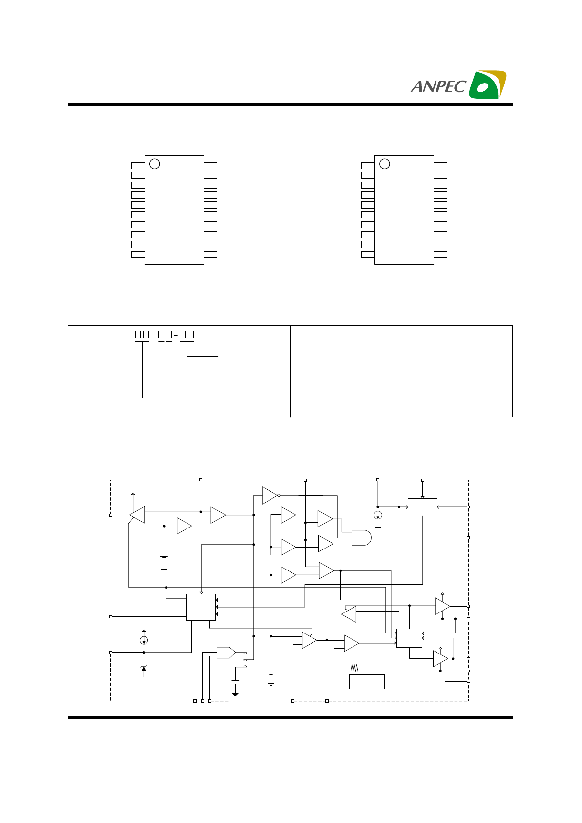
Pin Description
Ordering Information
Block Diagram
APW7035-12/19
PGOOD
LGATE
OCSET
PGND
UGATE
PHASEDRIVE
VCC
SS
VSEN1
VAUX
FB
COMP
1
1110
129
13
16
8
14
15
7
6
17
18
19
20
5
4
3
2
NCNC
NC
SD
VSEN2
NC
GND
VID0
LGATE
OCSET
PGND
UGATE
PHASEDRIVE
VCC
SS
VSEN1
VAUX
FB
COMP
1
1110
129
13
16
8
14
15
7
6
17
18
19
20
5
4
3
2
NCNC
VID1
SD
VSEN2
VID2
GND
APW7035A/B/C/D
APW7035
Voltage Code
12 : 1.25V 20 : 2.05V A : 1.00V~1.35V
B : 1.40V~1.75V C : 1.80V~2.40V D : 2.50V~3.20V
Package Code
K : SOP
Temp. Range
C : 0 to 70 C
Handling Code
TU : Tube TR : Tape & Reel
°
Handling Code
Temp. Range
Package Code
Voltage Code
PGOOD
Power-on
Reset (POR)
VCC
200mA
1.10
+
-
GATE
CONTROL
+
PWM
COMP1
SYNCH
DRIVE
OV
UGATE
PHASE
V
CC
LGATE
PGND
COMPFB
OCSETVSEN1
ERROR
AMP1
PWM1
VCC
INHIBIT
OC1
VAUX
DRIVE
+
-
+
-
+
-
+
-
0.90
1.15
VAUX
GND
VSEN2
+
-
0.75
+
-
1.5V
+
-
DAC
+
-
SOFT
START &
FAULT
LOGIC
SS
OSCILLATOR
INHIBIT
SD
V
CC
28mA
4.5V
DAC
+
-
VID0
VID1VID2
V
DAC
Page 3
Copyright ANPEC Electronics Corp.
Rev. A.4 - Jul., 2001
APW7035
www.anpec.com.tw3
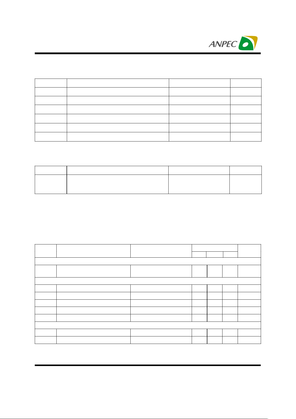
Absolute Maximum Ratings
Symbol Parameter Rating Unit
V
CC
Supply Voltage 15 V
VI , V
O
Input , Output or I/O Voltage GND -0.3 V to VCC +0.3 V
T
A
Operating Ambient Te mperature Range 0 to 70
°C
T
J
Junction Temperature Range 0 to 125
°C
T
STG
Storage Temperature Range -65 to +150
°C
T
S
Soldering Temperature 300 ,10 seconds
°C
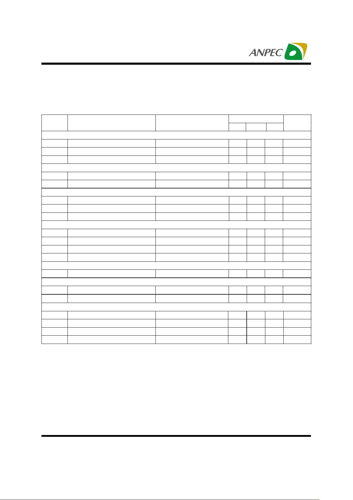
Electrical Characteristics
Thermal Characteristics
Symbol Parameter Value Unit
R
θ
JA
Thermal Resistance in Free Air
SOIC
SOIC (with 3in
2
of Copper)
75
65
°C/W
(Recommended operating conditions , Unless otherwise noted) Refer to Block and Simplified Power System
Diagrams , and Typical Application Schematic.
APW7035
Symbol Parameter Test Conditions
Min. Typ. Max.
Unit
VCC Supply Current
I
CC
Nominal Supply Current
UGATE, LGATE, DRIVE
open
9mA
Power-on Reset
Rising VCC Threshold Vocset=4.5V 10.7 V
Falling VCC Threshold Vocset=4.5V 8.2 V
Rising VAUX Threshold Vocset=4.5V 2.5 V
VAUX Threshold Hysteresis Vocset=4.5V 0.5 V
Rising V
OCSET
Threshold 1.26 V
Oscillator
F
OCS
Free Running Frequency RT= Open 185 200 215 kHz
∆
V
OSC
Ramp Amplitude RT= Open 1.9 V
P-P
Page 4
Copyright ANPEC Electronics Corp.
Rev. A.4 - Jul., 2001
APW7035
www.anpec.com.tw4
Electrical Characteristics Cont.
APW7035
Symbol Parameter Test Conditions
Min. Typ. Max.
Unit
DAC and Bandgap Reference
V
DAC
DACOUT Voltage accuracy -1.0 +1.0 %
V
BG
Bandgap Reference Voltage 1.265 V
Bandgap Reference Tolerance -2.5 +2.5 %
Linear Regulators
Regulation 3 %
Output Drive Current VAUX-V
DRIVE
>0.6V 20 40 mA
Synchronous PWM Controller Error Amplifier
DC Gain 88 dB
GBWP Gain-Bandwidth Produc t 15 MHz
SR Slew Rate COMP=10pF 6
V/µs
PWM Controller Gate Driver
I
UGATE
UGATE Source VCC=12V, V
UGATE
=6V 1 A
R
UGATE
UGATE Sink V
UGATE1-PHASE
=1V 3.5
Ω
I
LGATE
LGATE Source VCC=12V, V
LGATE
=1V 1 A
R
LGATE
LGATE Sink V
LGATE
= 1V 3
Ω
Protection
VSEN1 Over-Voltage VSEN1 Rising 115 120 %
Protection
I
OCSET
OCSET Current Source V
OCSET
= 4.5V
DC
170 200 230
µ
A
I
SS
Soft Start Current 28
µ
A
Power Good
VSEN1 Upper Threshold VSEN1 Rising 109 %
VSEN1 Under Voltage
VSEN1 Rising
93 %
VSEN1 Hysteresis Upper /Lower Threshold 2 %
V
PGOOD
PGOOD Voltage Low I
PGOOD
= -4mA 0.8 V
Functional Pin Description
(Recommended operating conditions , Unless otherwise noted) Refer to Block and Simplified Power System
Diagrams , and Typical Application Schematic.
VCC (Pin 1)
Provide a 12V bias supply for the IC to this pin. This
pin also provides the gate bias charge for all the
MOSFETs controlled by the IC. The voltage at this
pin is monitored for Power-On Reset (POR) purposes.
DRIVE (Pin 2)
Connect this pin to the gate of an external MOSFET.
This pin provides the drive for the FBVDDQ
regulator’s pass transistor.
Page 5

Copyright ANPEC Electronics Corp.
Rev. A.4 - Jul., 2001
APW7035
www.anpec.com.tw5
Functional Pin Description cont.
NC (Pin 3, Pin 4 and Pin 5)
No Connect. (APW7035-12,19)
PGOOD (Pin 5)
PGOOD is an open drain output used to indicate the
status of the output voltages. This pin is pulled low
when the synchronous regulator output is not within
±10% of the DAC reference voltage or Linear regula-
tor outputs are below under-voltage thresholds.
(APW7035-A,B,C,D)
VID2 , VID1 , VID0 (Pin 3,4 and 5)
VID0-2 are the TTL-compatible input pins to the 3-bit
DAC. The logic states of these three pins program
the internal voltage reference (DAC). The level of DAC
sets the microprocessor core converter output voltage , as well as the corresponding PGOOD and OVP
thresholds. (APW7035-A,B,C,D)
SD (Pin 6)
The pin shuts down all the outputs. A TLL-compatible
, logic lebel high signal applied at this pin immediately discharges the soft-start capacitor , disbling all
the output.
VSEN2 (Pin 7)
Connect this pin to a resistor divider to set the linear
regulator (FBVDDQ) output voltage.
SS (Pin 8)
Connect a capacitor from this pin to ground. This
capacitor , along with an internal 28µA current source
, sets the soft-start interval of the converter.
NC (Pin 9 and Pin12)
No Connection.
V AUX (Pin 10)
This pin provides boost current for the linear regulator’s
output drives in the event bipolar NPN transistors
(instead of N-channel MOSFETs) are employed as
pass elements. The voltage at this pin is monitored
for power-on reset purposes.
GND (Pin 11)
Signal ground for the IC. All voltage levels are measured with respect to this pin.
FB and COMP (Pin 13, and 14)
COMP and FB are the available external pins of the
PWM converter error amplifier. The FB pin is the
inverting input of the error amplifier. Similarly , the
COMP pin is the error amplifier output. These pins
are used to compensate the voltage-mode control
feedback loop of the synchronous PWM converter.
VSEN1 (Pin 15)
This pin is connected to the PWM converter’s output
voltage. The PGOOD and OVP comparator circuits
use this signal to report output voltage status and for
over- voltage protection.
OCSET (Pin 16)
Connect a resistor from this pin to the drain of the
respective upper MOSFET. This resistor , an internal 200µA current source , and the upper MOSFET’s
on-resistance set the converter over-current trip point.
An over-current trip cycles the soft-start function. The
voltage at this pin is monitored for power-on reset
(POR) purposes and pulling this pin low with an open
drain device will shutdown the IC.
PGND (Pin 17)
This is the power ground connection. Tie the synchronous PWM converter’s lower MOSFET source
to this pin.
LGATE (Pin 18)
Connect LGATE to the PWM converter’s lower
MOSFET gate. This pin provides the gate drive for
the lower MOSFET.
Page 6

Copyright ANPEC Electronics Corp.
Rev. A.4 - Jul., 2001
APW7035
www.anpec.com.tw6
Simplified Power System Diagram
PHASE (Pin 19)
Connect the PHASE pin to the PWM converter’s upper MOSFET source. This pin represents the gate
drive return current path and is used to monitor the
voltage drop across the upper MOSFET for over-current protection.
Functional Pin Description cont.
UGA TE (Pin 20)
Connect UGATE pin to the PWM converter’s upper
MOSFET gate. This pin provides the gate drive for
the upper MOSFET.
Table1 Output Voltage Program
VID2 VID1 VID0
APW7035-A
VID2 VID1 VID0
APW7035-B
0 0 0 1.35V 0 0 0 1.75V
0 0 1 1.30V 0 0 1 1.70V
0 1 0 1.25V 0 1 0 1.65V
0 1 1 1.20V 0 1 1 1.60V
1 0 0 1.15V 1 0 0 1.55V
1 0 1 1.10V 1 0 1 1.50V
1 1 0 1.05V 1 1 0 1.45V
1 1 1 1.00V 1 1 1 1.40V
VID2 VID1 VID0
APW7035-C
VID2 VID1 VID0
APW7035-D
0 0 0 2.40V 0 0 0 3.20V
0 0 1 2.30V 0 0 1 3.10V
0 1 0 2.20V 0 1 0 3.00V
0 1 1 2.10V 0 1 1 2.90V
1 0 0 2.00V 1 0 0 2.80V
1 0 1 1.90V 1 0 1 2.70V
1 1 0 1.80V 1 1 0 2.60V
11101112.50V
Linear Controller
PWM1
Controller
APW7035
V
OUT1
Q2
3.3 V
IN
Q1
V
OUT2
Q3
5.0V
IN
Page 7

Copyright ANPEC Electronics Corp.
Rev. A.4 - Jul., 2001
APW7035
www.anpec.com.tw7
Typical Application Circuit
SS COMP
8
7
2
10
6
13
15
14
19
18
17
20
5
16
VENS1
DRIVE
VAUX
SD
VCC
FB
VENS1
PGND
LGATE
PHASE
UGATE
PGOOD
OCSET
GND
11
1
C2
220pF
R4
1.2K
C3
330uF
C4
10uF
C6
330uF
R7
64
C5
330uF
L1
L2
Q2A
APM7313
Q2B
APM7313
R5
5.1
R6
5.1
R9
3K
R8
100
C7
10pF
R10
150K
C8
2700pF
C9
0.1uF
R3
100
C11
330uF
Q1
APM3055L
C10
330uF
C1
1uF
R1
10
12V
3.3V
2.5V
2.05V
5.0V
APW7035-12
R2
66.7
Page 8

Copyright ANPEC Electronics Corp.
Rev. A.4 - Jul., 2001
APW7035
www.anpec.com.tw8
Package Information
SO – 300mil ( Reference JEDEC Registration MS-013)
Millimet ers Varia t ions Inch es Varia t ions
Dim
Min. Max. Variations Min. Max.
Dim
Min. Max. Variations Min. Max.
A2.35
2.65
SO-20
12.60 13.0
A 0.093 0.1043 SO-20 0.496 0.512
A1
0.10 0.30
SO-24
15.20 15.60
A1 0.004 0.0120 SO -24 0.59 9 0.614
B
0.33 0.51
SO-28
17.70 18.11
B 0.013 0.020 SO-28 0.697 0.713
C 0.23 0.32 C 0.0091 0.0125
D See variations D See variations
E
7.40 7.60
E 0.2914
0.299
e 1.27BS C e 0.050BSC
H
10 10.65
H 0.394 0.41 9
h
0.25 0.75
h 0.010 0.029
L
0.40 1.27
L 0.016 0.050
φ
10°8
°φ
10°8
°
12
3
EH
D
L
GAUGE
PLANE
1
e
B
A1
A
C
h*45
Page 9

Copyright ANPEC Electronics Corp.
Rev. A.4 - Jul., 2001
APW7035
www.anpec.com.tw9
Classification Reflow Profiles
Package Reflow Conditions
Refolw Condition (IR/ Convection or VPR Reflow)
Physical Specifications
Terminal Material Solder-Plated Copper (Solder Material : 90/10 or 63/37 SnPb)
Lead Solderability Meets EIA Specification RSI86-91, ANSI/J-STD-002 Category 3.
Packaging 1000 devices per reel
Convection or IR/ Convection VPR
Average ramp-up rate(183°C to Peak) 3°C/second max. 10 °C /second max.
Preheat temperature 125 ± 25°C)
120 seconds max.
Temperature maintained above 183°C
60 ~ 150 seconds
Time within 5°C of actual peak
temperature
10 ~ 20 seconds 60 seconds
Peak temperature range
220 +5/-0°C or 235 +5/-0°C 215~ 219°C or 235 +5/-0°C
Ramp-down rate
6 °C /second max. 10 °C /second max.
Time 25°C to peak temperature
6 minutes max.
pkg. thickness ≥≥≥≥ 2.5mm
and all bags
pkg. thickness < 2.5mm and
pkg. volume ≥≥≥≥ 350 mm³
pkg. thickness < 2.5mm and pkg.
volume < 350mm³
Convection 220 +5/-0 °C Convection 235 +5/-0 °C
VPR 215-219 °C VPR 235 +5/-0 °C
IR/Convection 220 +5/-0 °C IR/Convection 235 +5/-0 °C
Reference JEDEC Standard J-STD-020A APRIL 1999
Pre-heat temperature
183 C
Peak temperature
Time
°
temperature
Page 10

Copyright ANPEC Electronics Corp.
Rev. A.4 - Jul., 2001
APW7035
www.anpec.com.tw10
Tape & Reel Dimensions
Reliability test program
Test item Method Description
SOLDERABILITY MIL-STD-883D-2003
245°C , 5 SEC
HOLT MIL-STD-883D-1005.7
1000 Hrs Bias @ 125 °C
PCT JESD-22-B, A102
168 Hrs, 100 % RH , 121°C
TST MIL-STD-883D-1011.9
-65°C ~ 150°C, 200 Cycles
ESD MIL-STD-883D-3015.7 VHBM > 2KV, VMM > 200V
Latch-Up JESD 78 10ms , Itr > 100mA
t
Ao
E
W
Po P
Ko
Bo
D1
D
F
P1
A
J
B
T2
T1
C
Application
A B C J T1 T2 W P E
SOP-20
330±1 62 ± 1.5
12.75
±
0.15
2 + 0.6 24.4 +0.2
2± 0.2
24 + 0.3
- 0.1
12± 0.1 1.75± 0.1
Application
F D D1 Po P1 Ao Bo Ko t
SOP-20
11.5 ± 0.1
1.5+0.1 1.5+0.25
4.0 ± 0.1 2.0 ± 0.1 8.2 ± 0.1 13± 0.1 2.5± 0.1 0.35±0.013
(mm)
Page 11

Copyright ANPEC Electronics Corp.
Rev. A.4 - Jul., 2001
APW7035
www.anpec.com.tw11
Cover Tape Dimensions
Customer Service
Anpec Electronics Corp.
Head Office :
5F, No. 2 Li-Hsin Road, SBIP,
Hsin-Chu, T aiwan, R.O.C.
T el : 886-3-5642000
Fax : 886-3-5642050
Taipei Branch :
7F, No. 137, Lane 235, Pac Chiao Rd.,
Hsin Tien City, T aipei Hsien, Taiwan, R. O. C.
T el : 886-2-89191368
Fax : 886-2-89191369
Carrier Width
24
Cover Tape Width
21.3
(mm)
 Loading...