

Page 1
Copyright ANPEC Electronics Corp.
Rev.a.2 - Sep., 2001
APW7026
www.anpec.com.tw1
ANPEC reserves the right to make changes to improve reliability or manufacturability without notice, and advise
customers to obtain the latest version of relevant information to verify before placing orders.
Advanced PWM and Dual Linear Power Control
Applications
Pin Description
1
2
3
4
5
6
7
8
9
10
20
19
18
17
16
15
14
13
12
11
UGATE1
VCC
UGATE2
PHA SE2
PG OOD
OCSET 2
FB2
V5
SS
FAULT/RT
PHA SE1
LGATE1
PG ND
OCSET 1
VSE N1
FB1
FB3
GAT E
GND
V3.3
•
VGA Card Power Regulation
Features
••
••
•
3 Regulated Voltage are provided
••
••
• SYNC Switching Power for VTT(1.25V)
••
••
• ASYNC Switching Power for NVVDD(2.05V)
••
••
• Linear Regulator for FBVDDQ(2.5V)
••
••
•
Simple Single-Loop Control Design
••
••
• Voltage-Mode PWM Control
••
••
•
Excellent Output Voltage Regulation
••
••
• VTT Output: ±1% Over Temperature
••
••
• NVVDD Output: ±2% Over Temperature
••
••
• FBVDDQ Output:±2.5% Over Temperature
••
••
• Fast Transient Response
••
••
• On-Chip Feedback Compensation
••
••
• Full 0% to 100% Duty Ratio
••
••
• Power-Good Output Voltage Monitor
••
••
• Over-Voltage and Over-Current Fault Monitors
••
••
• Small Converter Size
••
••
• Constant Frequency Operation(200kHz)
••
••
• Programmable Oscillator from 50kHz to
800KHz
••
••
• Reduce External Component Count
General Description
The APW7026 Provides the power control and
protection for three output voltages in VGA Card
applications. It integrates two PWM controllers, one
linear controller as well as the monitoring and
protection functions into a single package. One PWM
controller (PWM1) regulates the termination voltage
VTT(1.25V) with a synchronous-rectified buck
converter. The second PWM controller (PWM2)
supplies the Core power NVVDD ( 2.05V ) with a
standard buck converter . The linear controller
regulates 2.5V power for FBVDDQ.
The APW7026 can monitor all the output voltages
(VTT ,NVVDD,FBVDDQ) and a single power good
signal is issued when the VTT is within ± 10% of
the reference voltage (VREF1) and the other levels
are above its lower power good threshold voltage.
Additional built-in overvoltage protection (OVP) will
be started when the VTT output is above 118% of
the VREF1.The OVP function will shutdown the upper
MOSFET and turn on the lower MOSFET
until the over-voltage is disappeared. The PWM
controllers over-current function monitors the output current by sensing the voltage drop across the
upper MOSFET rDS(ON), eliminating the need for a
current sensing resistor.
Page 2
Copyright ANPEC Electronics Corp.
Rev. A.2 - Sep., 2001
APW7026
www.anpec.com.tw2
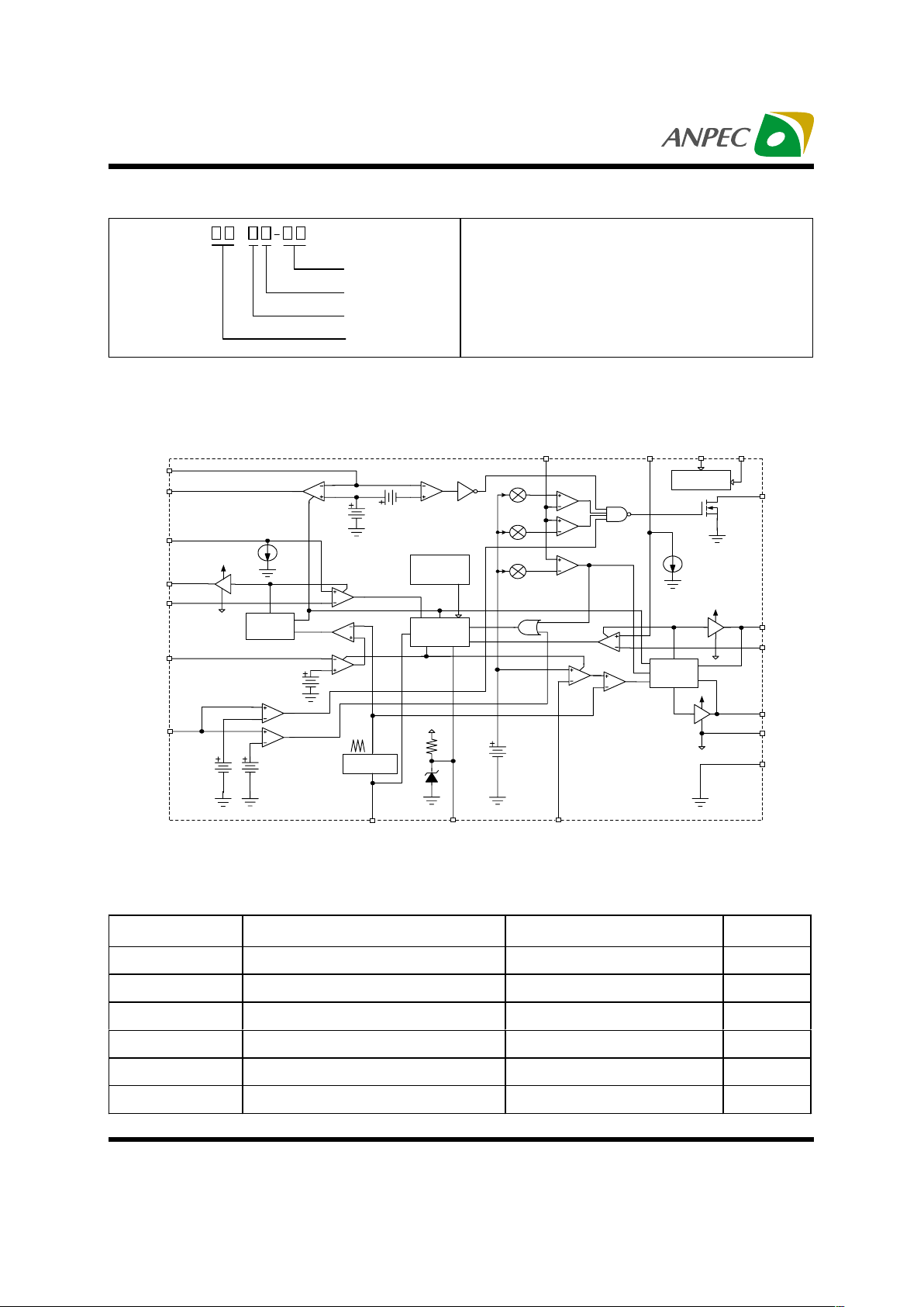
Block Diagram
Absolute Maximum Ratings
Ordering information
Symbol Parameter Rating Unit
VCC Supply Voltage 15 V
VI , V
O
Input , Output or I/O Voltage GND -0.3 V to VCC +0.3 V
T
A
Operating Ambient Temperature Range 0 to 70
o
C
T
J
Junction Temperature Range 0 to 125
o
C
T
STG
Storage Temperature Range -65 to +150
o
C
T
S
Soldering Temperature 300 ,10 seconds
o
C
APW7026
Voltage Code
12 : 1.2 5V
Package Code
K : SOP - 2 0
Te m p. R a ng e
C : 0 to 70
°
C
Handling Code
TU : Tu be TR : Tape & Ree l
Handling Code
Te m p. R a ng e
Package Code
Voltage Code
GATE
CONTROL
SOFT-START
AND FAULT
LOGIC
THERMAL
PROTECTION
GATE
CONTROL
POWER-ON
RESET
FB3
GATE
OCSET2
UGATE2
PHASE2
FB2
V3.3
GND
PGND
LGATE1
PHASE1
UGATE1
PGOOD
V5VCCOCSET1VSEN1
FB1SSFAULT/RT
0.3V
V
4-.!
1.26V
200uA
VCC
DRIVE2 OC2
INHIBIT
PWM2
V
4-.
2.0V
ERROR
AMP2
2.5V 4.1V
5V
OSCILLATOR
23K
4.6V
V
4-.
ERROR
AMP1
0V
FAULT
OC1
PWM1
VCC
LOW ER
DRIVE
VCC
DRIVE1
INHIBIT
118%
90%
110%
200uA
LUV
Page 3
Copyright ANPEC Electronics Corp.
Rev. A.2 - Sep., 2001
APW7026
www.anpec.com.tw3
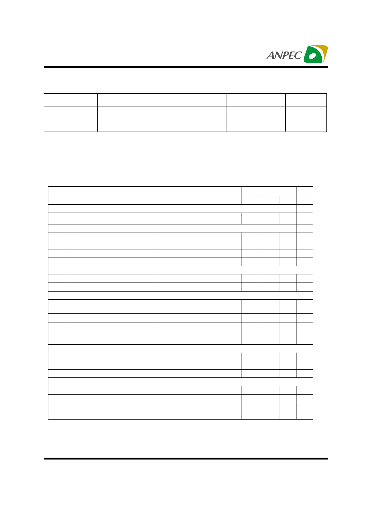
Electrical Characteristics
Thermal Characteristics
Symbol Parameter Value Unit
R
JA
Thermal Resistance in Free Air
SOIC
SOIC (with 3in
2
of Copper)
75
65
o
C
1. Recommended operating conditions, Unless otherwise noted.
2. Refer to Block and Simplified Power System Diagrams , and Typical Application Schematic.
APW7026 Unit
Symbol Parameter Test Conditions
Min Typ Max
SUPPLY CURRENT
I
CC
Nominal Supply Current
UGATE1, LGATE1, UGATE2, and
GATE Open
6mA
POWER-ON RESET
Rising VCC Threshold 9.5 10.4 V
Falling VCC Threshold 8.2 9.0 V
Rising V5 Threshold 4.4 4.7 V
Falling V5 Threshold 3.7 4.0 V
OSCILLATOR
F
OSC
Free Running Frequency RT = Open 185 200 215 kHz
∆
V
OSC
Ramp Amplitude RT = Open 1.9 V
PWM CONTROLLER REFERENCE VOLTAGE
V
REF1
SYNC PWM Controller Reference
Volta ge
1.25 V
V
REF1
Accuracy -1 +1 %
V
REF2
ASYNC PWM Controller Reference
Volta ge
2.0 V
V
REF2
Accuracy -2 +2 %
LINEAR CONTROLLER
V
REF3
Reference Voltage GATE=FB3 1.26 V
V
REF3
Accuracy -2.5 +2.5 %
GATE Drive Current V
GATE
=4V 20 50 mA
PWM CONTROLLERS GATE DRIVERS
I
UGATE
UGATE1,2 Source VCC = 12V, V
UGATE1
(or V
UGATE2
) = 6V 1.0 A
R
UGATE
UGATE1,2 Sink VCC = 12V, V
UGATE1
(or V
UGATE2
) = 1V 2.2 3.5
Ω
I
LGATE
LGATE1 Source VCC = 12V, V
LGATE1
= 1V 1.0
A
R
LGATE
LGATE1 Sink VCC = 12V, V
LGATE1
= 1V 1.6 3.0
Ω
Page 4
Copyright ANPEC Electronics Corp.
Rev. A.2 - Sep., 2001
APW7026
www.anpec.com.tw4
Electrical Characteristics Cont.
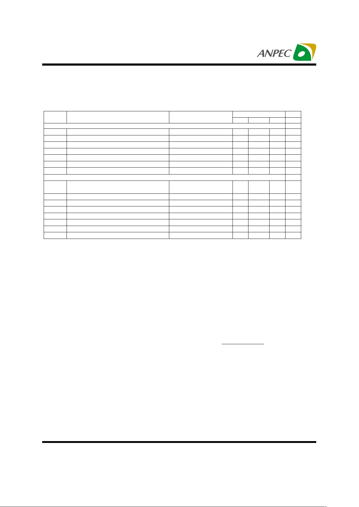
Functional Pin Description
1. Recommended operating conditions, Unless otherwise noted.
2. Refer to Block and Simplified Power System Diagrams , and Typical Application Schematic.
AP W 7026 Unit
Sym bol Param eter Test Conditions
Min Typ Max
PROTECTION
V S E N 1 O .V. tr ip p o int (V S E N 1/V
REF1
)
VSEN 1 Rising
118 %
VSEN1 O.V. Hysteresis 2%
V 3 .3 O .V. trip p o in t V 3 .3 R is in g 4 .1 V
V 3 .3 O .V. H y s te re s is 0.1 V
l
OVP
FAULT Souring Current V
FAU LT/RT
= 2.0V 25 m A
O C S E T 1 ,2 C urre n t S o urc e Vo cse t = 4.5V 170 200 230 uA
R
SS
Pull up resistor to 5V 23
K
Ω
POWER GOOD
VSEN1 Upper Threshold
(V S E N 1/V
REF1
)
VSEN1 Rising 110 %
VSEN 1 Lower Threshold VSEN 1 Rising 94 %
VSEN 1 PG D Hysteresis Upper/Lower Threshold 2 %
V 3 .3 L ow er T h re s h o ld V 3 .3 R is in g 2.5 V
V 3 .3 P G D H ys te re s is 0.1 V
FB3 Lower Threshold V
FB3
R is in g 1 .0 V
FB3 PG D Hysteresis 0.1 V
V
PGOOD
PGOOD Voltage Low l
PGOOD
= -4 m A 0 .8 V
UGATE1 (Pin 1)
Connect UGATE1 pin to the SYNC PWM Converters
upper MOSFET gate .This pin provides the gate drive
for the upper MOSFET.
VCC (Pin 2)
Provide a + 12V bias supply for the IC to this pin . This
pin also provides the gate bias charge for all the
MOSFETs controlled by the IC. The voltage at this pin is
monitored for Power-On Reset (POR) purpose.
UGATE2 (Pin 3)
Connect UGATE2 pin to the ASYNC PWM converters
MOSFET gate . This pin provides the gate drive for the
MOSFET.
PHASE2 (Pin 4)
Connect the PHASE2 pin to the ASYNC PWM
converters MOSFET source. This pin is used to monitor
the voltage drop across the MOSFET for over-current
protection.
PGOOD (Pin 5)
PGOOD is an open drain output used to indicate the
status of the output voltages. This pin is pulled low when
the SYNC PWM regulator output is not within ± 10%
of the reference voltage (V
REF1
) or when V3.3 or V
FB3
is
below its lower power good threshold.
OCSET2 (Pin 6)
Connect a resistor (R
OCSET
) from this pin to the drain of
the ASYNC PWM converters MOSFET . R
OCSET
, an
internal 200
µA current source (I
OCSET
) , and the
MOSFETs on-resistance (r
DS(ON)
) set the converters
over-current (OC) trip point according to the following
equation:
I
PEAK
=
An over-current trip cycles the soft-start function.
FB2 (Pin 7)
Connect this pin to the output of the ASYNC PWM
converter . The voltage at this pin is regulated to the
reference voltage V
REF2
. A resistor driver is connected
from this pin to V
OUT2(ROUT2
) and to GND(R
GND2
) that sets
the output voltage as the following equation :
1
OCSET
N 4
OCS ET
H
DS(ON)
Page 5

Copyright ANPEC Electronics Corp.
Rev. A.2 - Sep., 2001
APW7026
www.anpec.com.tw5
Functional Pin Description Cont.
V
OUT2
=
The value of the resistor connected from V
OUT2
to FB2 must
be less than 150Ω .
V5 (Pin 8)
The +5V input voltage at this pin is monitored for power-on
reset (POR) purpose.
SS (Pin 9)
This pin provides the soft-start for the all PWM converters
and linear regulator . An internal resistor charges an
external capacitor that is connected from 5V supply to
this pin which ramps up the all outputs , preventing the
outputs from overshooting as well as limiting the input
current . The second function of the soft-start cap is to
provides long off time for the synchronous MOSFET during
current limiting .
FAULT / RT (Pin 10)
This pin provides oscillator switching frequency
adjustment . By placing a resistor ( R
T
) from this pin to
GND , the nominal 200kHz switching frequency is
increased .Conversely, connecting a pull-up resistor ( R
T
)
from this pin to VCC reduces the switching frequency.
Nominally , the voltage at this pin is 1.26V. In the event of
an over-voltage or over-current condition , this pin is
internally pulled to VCC.
V3.3 (Pin 11)
This pin is connected to the +3.3V or the output of the
ASYNC PWM converter for power good and
over-voltage detection. When the output voltage of the
ASYNC PWM converter is not in the range from 3V to
4V, connect this pin to +3.3V voltage.
GND (Pin 12)
Signal ground for the IC. All voltage levels are measured
with respect to this pin.
GATE (Pin 13)
Connect this pin to the gate of an external MOSFET.
This pin provides the drive for the linear regulators
R
OUT2
R
GND2
( 1+ ) x V
REF2
pass MOSFET.
FB3 (Pin 14)
Connect this pin to the output of the linear regulator . A
resistor driver is connected from this pin to V
OUT3
and
GND that sets the output voltage as same as V
OUT2
. This
pin is monitored for power good function.
FB1 (Pin 15)
This pin provides the feedback for the SYNC PWM
converter. Typically this pin can be connected directly to
the output of the converter . However , a resistor
divider is recommended to be connected from this pin to
V
OUT1
and GND to adjust the output voltage as same as
V
OUT2
. The value of the resistor connected from V
OUT1
to
FB1 must be less than 200Ω.
VSEN1 (Pin 16)
This pin is connected to the SYNC PWM converters
output voltage . The PGOOD and OVP comparator
cicuits use this signal to report output voltage status
and over-voltage protection.
OCSET1 (Pin 17)
Connect a resistor (R
OCSET
) from this pin to the drain of
the SYNC PWM converters upper MOSFET . The
over-current (OC) trip point for the SYNC PWM
converter is set by the R
OCSET
as same as the OCSET2.
An over-current trip cycles the soft-start function.
PGND (Pin 18)
This is the power ground connection . Tie the SYNC
PWM converters lower MOSFET source to this pin.
LGATE1 (Pin 19)
Connect LGATE1 to the SYNC PWM converters lower
MOSFET gate . This pin provides the gate drive for the
lower MOSFET.
PHASE1 (Pin 20)
Connect the PHASE1 pin to the SYNC PWM
Converters upper MOSFET source. This pin is used
to monitor the voltage drop across the upper MOSFET
for over-current protection.
Page 6

Copyright ANPEC Electronics Corp.
Rev. A.2 - Sep., 2001
APW7026
www.anpec.com.tw6
Typical Performance Curves
# # # !# "# ## $# %#
Switching Frequency ( kHz )
-1.0%
-0.8%
-0.6%
-0.4%
-0.2%
0.0%
0.2%
0.4%
0.6%
0.8%
1.0%
0255075100125
Reference Voltage Deviation(V
4-.
)
Junction Tempe rature (oC)
-1.0%
-0.8%
-0.6%
-0.4%
-0.2%
0.0%
0.2%
0.4%
0.6%
0.8%
1.0%
0255075100125
Reference Voltage Deviation(V
4-.
)
Junction Temperature (oC)
-1.0%
-0.8%
-0.6%
-0.4%
-0.2%
0.0%
0.2%
0.4%
0.6%
0.8%
1.0%
0255075100125
Note : The Referance Voltage(V
REF
) Deviation is
Junction Tempe rature (oC)
V
REF(TJ
) - V
REF
(25oC)
V
REF
(25oC)
x 100%
RT ( k
Ω
ΩΩ
Ω
)
RT pull up
to +12V
RT pull down to G ND
Reference Voltage Deviation(V
4-.
)
HJ
TJ is Junction Temperature.
Page 7

Copyright ANPEC Electronics Corp.
Rev. A.2 - Sep., 2001
APW7026
www.anpec.com.tw7
Typical Application Circuit
UGATE1
PGOOD
PHASE2
UGATE2
VCC
SS
FB2
OCSET2
V5 FB3
VSEN1
FB1
GATE
LGATE1
PGND
OCSET1
PHASE1
1
7
6
5
4
3
2
13
14
15
16
17
18
19
20
12
11
+5V
NVVDD
2.05V/4A
VTT
1.25V/3.5A
AGP
3.3V
+12V
AGP
3.3V
FBVDDQ
2.5V/1.5A
C807
330uF
C808
330uF
R812
1.5k
C809
220pF
R813
5.1R
Q802
APM9410
D800
FM5820
C811
330uF
R814
100RF
C810
330uF
R810
97.6RF
C817
330uF
Q800
APM3055
C802
330uF
R820
5.1R
Q803B
APM7313
C815
330uF
C816
330uF
C814
10uF
C813
330uF
L802
2uH
L803
7.8uH
Q803A
APM7313
C812
220pF
R817
1.2K
R819
5.1R
C801
1uF
RX1
10R
L801
7.8uH
L800
2uH
APW7026-12
R811
100RF
10
9
8
5V
C805
1uF
R816
4.02KF
FAULT/RT
GND
V3.3
R821
0R
R824
NC
Simplified Power System Diagram
V
OUT1
Q1
Q2
Q3
Q4
V
OUT3
+3.3V
ASYNC
PWM
C o ntro ller
Linear
C o ntro ller
SYNC
PWM
C o ntro ller
+3.3v
V
OUT2
+5V
Page 8

Copyright ANPEC Electronics Corp.
Rev. A.2 - Sep., 2001
APW7026
www.anpec.com.tw8
SO 300mil ( Reference JEDEC Registration MS-013)
Millimeters Variations- D Inches Variations- D
Dim
Min. Max. Variations Min. Max.
Dim
Min. Max. Variations Min. Max.
A2.35
2.65
SO-16
10.10 10.50
A 0.093 0.1043 SO-16 0.398 0.413
A1
0.10 0.30
SO-18
11. 35 11 .76
A1 0.004 0.0120 SO-18 0.447 0.463
B
0.33 0.51
SO-20
12.60 13
B 0.013 0.020 SO-20 0.496 0.512
D See variations SO-24
15.20 15.60
D See variations SO-24 0.599 0.614
E
7.40 7.60
SO-28
17.70 18.11
E 0.2914 0.2992 SO-28 0.697 0.713
e 1.27BSC SO-14
8.80 9.20
e 0.050BSC SO-14 0.347 0.362
H
10 10.65
H 0.394 0.419
L
0.40 1.27
L 0.016 0.050
N See variations N See variations
φ
1 0
°
8
°φ
10°8
°
N
12
3
EH
D
L
GAUGE
PLANE
1
e
B
A1
A
Page 9

Copyright ANPEC Electronics Corp.
Rev. A.2 - Sep., 2001
APW7026
www.anpec.com.tw9
Classification Reflow Profiles
Package Reflow Conditions
Refolw Condition (IR/ Convection or VPR Reflow)
Physical Specifications
Terminal Material Solder-Plated Copper (Solder Material : 90/10 or 63/37 SnPb)
Lead Solderability Meets EIA Specification RSI86-91, ANSI/J-STD-002 Category 3.
Packaging 1000 devices per reel
Convection or IR/ Convection VPR
Average ramp-up rate(183°C to Peak) 3°C/second max. 10 °C /second max.
Preheat temperature 125 ± 25°C)
120 seconds max.
Temperature maintained above 183°C
60 ~ 150 seconds
Time within 5°C of actual peak
temperature
10 ~ 20 seconds 60 seconds
Peak temperature range
220 +5/-0°C or 235 +5/-0°C 215~ 219°C or 235 +5/-0°C
Ramp-down rate
6 °C /second max. 10 °C /second max.
Time 25°C to peak temperature
6 minutes max.
pkg. thickness ≥≥≥≥ 2.5mm
and all bags
pkg. thickness < 2.5mm and
pkg. volume ≥≥≥≥ 350 mm³
pkg. thickness < 2.5mm and pkg.
volume < 350mm³
Convection 220 +5/-0 °C Convection 235 +5/-0 °C
VPR 215-219 °C VPR 235 +5/-0 °C
IR/Convection 220 +5/-0 °C IR/Convection 235 +5/-0 °C
Reference JEDEC Standard J-STD-020A APRIL 1999
Pre-heat temperature
183 C
Peak temperature
Time
°
temperature
Page 10

Copyright ANPEC Electronics Corp.
Rev. A.2 - Sep., 2001
APW7026
www.anpec.com.tw10
Tape & Reel Dimensions
Reliability test program
Test item Method Description
SOLDERABILITY MIL-STD-883D-2003
245°C , 5 SEC
HOLT MIL-STD-883D-1005.7
1000 Hrs Bias @ 125 °C
PCT JESD-22-B, A102
168 Hrs, 100 % RH , 121°C
TST MIL-STD-883D-1011.9
-65°C ~ 150°C, 200 Cycles
ESD MIL-STD-883D-3015.7 VHBM > 2KV, VMM > 200V
Latch-Up JESD 78 10ms , Itr > 100mA
t
Ao
E
W
Po P
Ko
Bo
D1
D
F
P1
A
J
B
T2
T1
C
Application
A B C J T1 T2 W P E
SOP-20 330±1 62 ± 1.5
12.75
±
0.15
2 + 0.6 24.4 +0.2
2± 0.2
24 + 0.3
- 0.1
12± 0.1 1.75± 0.1
Application
F D D1 Po P1 Ao Bo Ko t
SOP-20
11.5 ± 0.1
1.5+0.1 1.5+0.25
4.0 ± 0.1 2.0 ± 0.1 8.2 ± 0.1 13± 0.1 2.5± 0.1 0.35±0.013
(mm)
Page 11

Copyright ANPEC Electronics Corp.
Rev. A.2 - Sep., 2001
APW7026
www.anpec.com.tw11
Customer Service
Anpec Electronics Corp.
Head Office :
5F, No. 2 Li-Hsin Road, SBIP,
Hsin-Chu, Taiwan, R.O.C.
Tel : 886-3-5642000
Fax : 886-3-5642050
Taipei Branch :
7F, No. 137, Lane 235, Pac Chiao Rd.,
Hsin Tien City, Taipei Hsien, Taiwan, R. O. C.
Tel : 886-2-89191368
Fax : 886-2-89191369
Cover Tape Dimensions
Carrier Width
24
Cover Tape Width
21.3
(mm)
 Loading...