

Page 1

APW6021
Advanced PWM and Triple Linear Power Controllers
Functional
••
•
4 Regulated Voltages are provided
••
••
• Microprocessor Core (1.3V to 3.5V)
••
••
• AGP Bus (1.5V or 3.3V)
••
••
• Memory (1.8V)
••
••
• GTL Bus (1.5V)
••
••
•
Linear Controllers Drives with both MOSFET
••
and Bipolar Series Pass Transistors
••
• Fixed or Externally Resistor-Adjustable Linear
••
Outputs (FIX Pin)
••
• Simple Single-Loop Control Design
••
••
• Voltage-Mode PWM Control
••
••
• Fast PWM Converter Transient Response
••
••
• High-Bandwidth Error Amplifier
••
••
• Full 0% to 100% Duty Ratio
••
••
• Excellent Output Voltage Regulation
••
••
• Core PWM Output: ± 1% Over Temperature
••
••
• Other Outputs: ± 3% Over Temperature
••
••
• TTL-Compatible 5- Bit DAC Microprocessor
••
Core Output Voltage Selection
••
• Wide Range - 1.3VDC to 3.5 V
••
••
• Power-Good Output Voltage Monitor
••
••
• Over-Voltage and Over-Current Fault Monitors
••
••
• Switching Regulator Does Not Require
••
DC
Applications
••
•
Motherboard Power Regulation for Computers
••
General Description
The APW6021 provides the power control and protection for four output voltages in high-performance,
graphics intensive microprocessor and computer
applications. The IC integrates voltage-mode PWM
controller and three linear controllers, as well as the
monitoring and protection functions into a 28-pin SOIC
package. The PWM controller regulates the microprocessor core voltage with a synchronous-rectified
buck converter. The linear controllers regulate the
computer system’s AGP 1.5V or 3.3V bus power, the
1.5V GTL bus power, and the 1.8V power for the
North/South Bridge core voltage and/or cache
memory circuits. The APW6021 includes an Intelcompatible, TTL 5-input digital-to-analog converter
(DAC) that adjusts the core PWM output voltage from
1.3 VDC to 2.05 VDC in 0.05V steps and from 2.1 VDC to
3.5 VDC in 0.1V increments. The precision reference
and voltage-mode control provide ±1% static
regulation. The AGP bus power linear controller’s
output (V
patible signal applied at the SELECT pin, for levels of
1.5V or 3.3V with ±3% accuracy. Based on the status of the FIX pin, the other two linear regulators provide either fixed output voltages of 1.5V± 3% (V
and 1.8V±3% (V
of an external resistor divider. All linear controllers
can employ either N-channel MOSFETs or bipolar
NPNs for the pass transistor.
) is user-selectable, through a TTL-com-
OUT2
), or user-adjustable by means
OUT4
OUT3
)
Extra Current Sensing Element, Uses
MOSFET’s r
••
• Small Converter Size
••
••
• Constant Frequency Operation
••
••
• 200kHz Free-Running Oscillator; Program-
••
mable From 50kHz to Over 1MHz
ANPEC reserves the right to make changes to improve reliability or manufacturability without notice, and advise
customers to obtain the latest version of relevant information to verify before placing orders.
Copyright ANPEC Electronics Corp.
Rev. P.4 - Mar., 2001
DS(ON)
The APW6021 monitors all the output voltages. A
single Power Good signal is issued when the core is
within ±10% of the DAC setting and all other outputs
are above their under-voltage levels. Additional builtin over-voltage protection for the core output uses
the lower MOSFET to prevent output voltages above
115% of the DAC setting. The PWM controller’s overcurrent function monitors the output current by using
the voltage drop across the upper MOSFET’s r
www.anpec.com.tw1
DS(ON)
.
Page 2
APW6021
Pin Description
DRIVE2
FIX
VID4
VID3
VID2
VID1
VID0
PGOOD
SD
VSEN2
SELECT
SS
FAULT/ RT
VSEN4
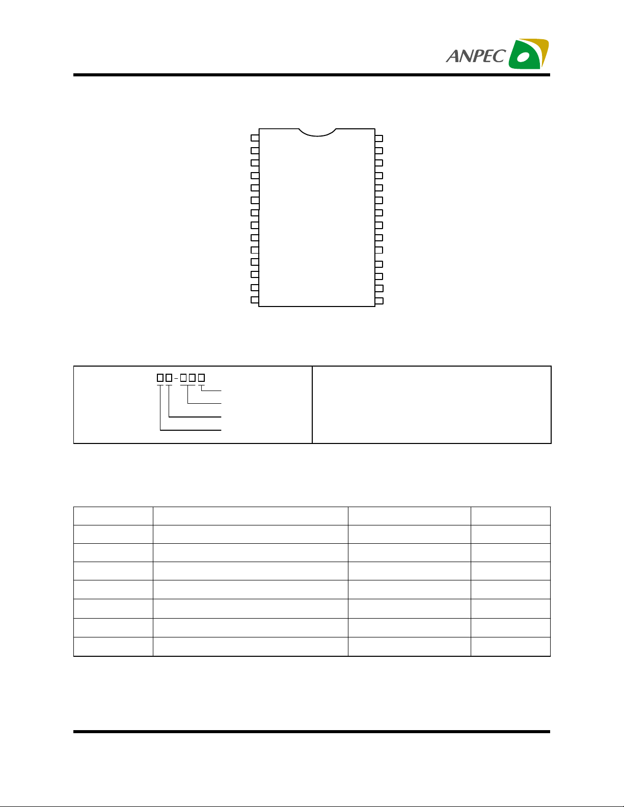
Ordering Information
APW 6021
Lead Free Code
Handling Code
Tem p. Range
Package Code
1
2
3
4
5
6
7
8
9
10
11
12
13
14
28
27
26
25
24
23
22
21
20
19
18
17
16
15
Package Code
K : S O P - 2 8
Tem p. Range
C : 0 to 7 0 C
Handling Code
TU : Tube TR : Tape & Reel
Lead Free Code
L : Lead Free Device Blank : Original Device
VCC
UGATE
PHASE
LGATE
PGND
OCSET
VSEN1
FB
COMP
VSEN3
DRIVE3
GND
VAUX
DRIVE4
°
Absolute Maximum Ratings
Symbol Parameter Rating Unit
V
CC
V
–V
BOOT
Copyright ANPEC Electronics Corp.
Rev. P.4 - Mar., 2001
VI , V
T
T
T
STG
T
PHASE
O
A
J
S
Supply Voltage 15 V
Boot Voltage 15 V
Input , Output or I/O Voltage GND -0.3 V to VCC +0.3 V
Operating Ambient Temperature Range 0 to 70
Junction Temperature Range 0 to 125
Storage Temperature Range -65 to +150
Soldering Temperature 300 ,10 seconds
C
°
C
°
C
°
C
°
www.anpec.com.tw2
Page 3
APW6021
Thermal Characteristics
Symbol Parameter Value Unit
Thermal Resistance in Free Air
R
JA
θ
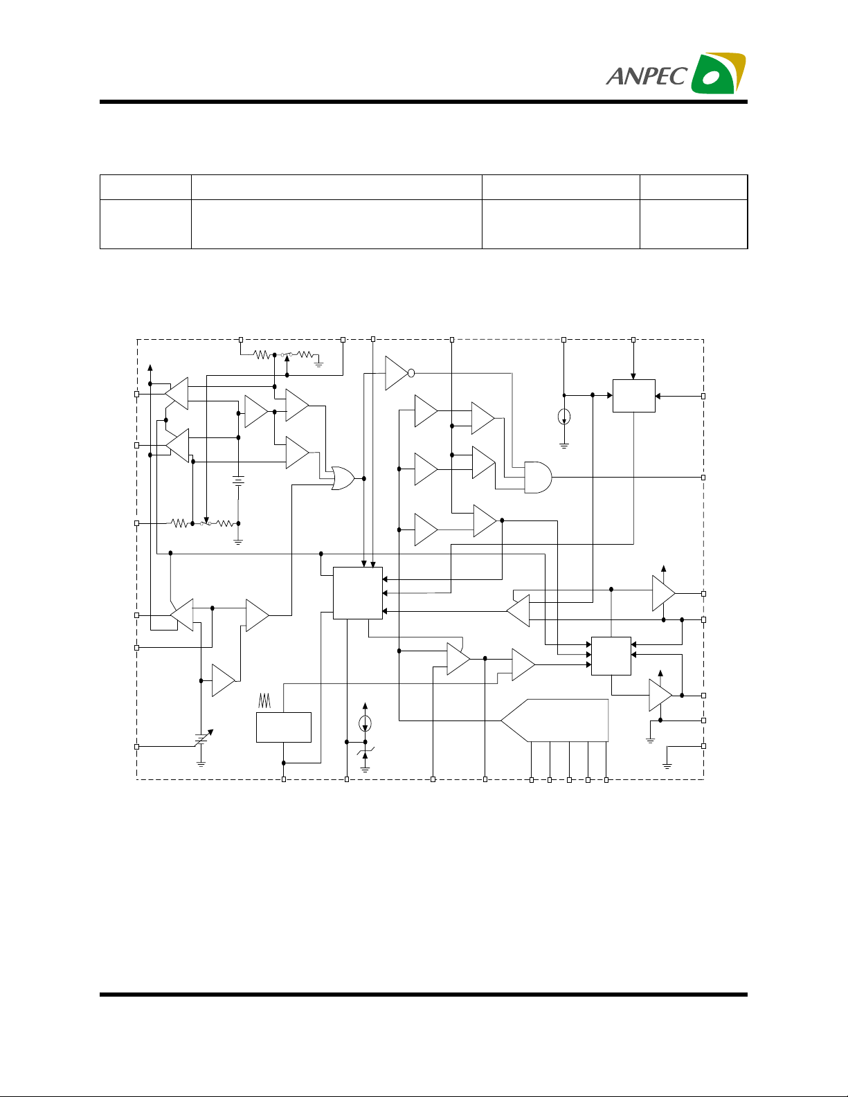
Block Diagram
SOIC
SOIC (with 3in
2
of Copper)
75
65
C/W
°
DRIVE3
DRIVE 4
VSEN 4
DRIVE2
VSEN2
SELECT
VAUX
INHIBIT
GATE
CONTROL
VCC
Power-on
Reset
(POR)
DRIVER1
SYNCH
DRIVE
VAUX
PGOOD
VCC
UGATE
PHASE
VCC
LGATE
PGND
GND
200µA
+
-
+
-
PWM
COMP1
CONVERTER
OCSETVSEN1
PWM1
TTL D/A
(DAC)
SDFIXVSEN3
+
+
-
+
-
+
×
0.75
1.5V
+
or
-
3.3v
×
0.75
1.26V
+
-
OSCILLATOR
+
+
-
LINEAR
UNDER-
VOLTAGE
INHIBIT
FAULT
LUV
SOFT START
& FAULT
LOGIC
VCC
28µA
4.5V
OV
DACOUT
×
1.10
×
0.90
×
1.15
ERROR
AMP1
+
-
+
-
+
-
OC1
+
-
FAULT/ RT
Copyright ANPEC Electronics Corp.
Rev. P.4 - Mar., 2001
VID1 VID2 VID3 VID4
COMPFBSS
VID0
www.anpec.com.tw3
Page 4

APW6021
Electrical Characteristics
(Recommended operating conditions, Unless otherwise noted) Refer to Block and Simplified Power
System Diagrams, and Typical Application Schematic
APW6021
Symbol Parameter Test Conditions
Min. Typ. Max.
VCC Supply Current
I
Nominal Supply Current
CC
UGATE, LGATE, DRIVE2,
DRIVE3, and DRIVE4 open
9mA
Power-on Reset
Rising VCC Threshold Vocset=4.5V 10.4 V
Falling VCC Threshold Vocset=4.5V 8.2 V
Rising VAUX Threshold Vocset=4.5V 2.5 V
VAUX Threshold Hysteres is Vocset=4.5V 0.5 V
Rising V
Threshold 1.26 V
OCSET
Oscillator
F
V
∆
Free Running Frequency RT= Open 185 200 215 kHz
OCS
Ramp Amplitude RT= Open 1.9 V
OSC
DAC and Bandgap Reference
DAC(VID0-VID4) Input Low
Voltage
DAC(VID0-VID4) Input High
Voltage
2.0 0.8 V
0.8 V
DACOUT Voltage accuracy -1.0 +1.0 %
V
Bandgap Reference Voltage 1.265 V
BG
Bandgap Reference Tolerance -2.5 +2.5 %
Linear Regulators (OUT2, OUT3, and OUT4)
Regulation (All Linears) 3 %
VREG2VSEN2 Regulation Voltage Select < 0.8V 1.5 V
VREG2VSEN2 Regulation Voltage Select > 2.0V 3.3 V
VREG3VSEN3 Regulation Voltage 1.5 V
VREG4VSEN4 Regulation Voltage 1.8 V
VREN
Under-Voltage Level (VSEN/
UV
VREG)
Under-Voltage Hysteresis (VSEN/
VREG)
Output Drive Current (All Liners) VAUX-V
VSEN Rising 75 %
VSEN Falling 7 %
>0.6V 20 40 mA
DRIVE
Unit
P-P
Copyright ANPEC Electronics Corp.
Rev. P.4 - Mar., 2001
www.anpec.com.tw4
Page 5

APW6021
Electrical Characteristics Cont.
APW6021
Symbol Parameter Test Conditions
Min. Typ. Max.
Synchronous PWM Controller Error Amplifier
DC Gain 88 dB
GBWP Gain-Bandwidth Prod uct 15 MHz
SR Slew Rate COMP=10pF 6
PWM Controller Gate Driver
I
UGATE
R
I
LGATE
R
UGATE
LGATE
UGATE Source VCC=12V, V
UGATE Sink V
UGATE1-PHASE
LGATE Source VCC=12V, V
LGATE Sink V
= 1V 3
LGATE
=6V 1 A
UGATE
=1V 3.5
=1V 1 A
LGATE
Protection
I
OVP
I
OCSET
I
VSEN1 Over-Voltage
(VSEN1/DACOUT)
FAULT Souring Current V
OCSET1 Current Source V
Soft Start Current 28
SS
VSEN1 Rising 115 120 %
=2.0V 8.5 mA
FAULT/RT
OCSET
= 4.5V
DC
170 200 230
Power Good
V
PGOOD
VSEN1 Upper Threshold
(VSEN1/DACOUT)
VSEN1 Under Voltage
(VSEN1/DACOUT)
VSEN1 Hysteresis (VSEN1
/DACOUT)
PGOOD Voltage Low I
VSEN1 Rising
VSEN1 Rising 92 94 %
Upper /Lower Threshold 2 %
= -4mA 0.8 V
PGOOD
108 110 %
Unit
V/µs
Ω
Ω
A
µ
A
µ
Functional Pin Description
DRIVE2 (Pin 1)
Connect this pin to the gate of an external MOSFET.
This pin provides the drive for the AGP regulator’s
pass transistor.
FIX (Pin 2)
Grounding this pin bypasses the internal resistor dividers that set the output voltage of the 1.5V and 1.
8V linear regulators. This way, the output voltage of
the two regulators can be adjusted from 1.26V up to
the input voltage (+3.3V or +5V) by way of an exter-
Copyright ANPEC Electronics Corp.
Rev. P.4 - Mar., 2001
nal resistor divider connected at the corresponding
VSEN pin. The new output voltage set by the external resistor divider can be determined using the following formula:
V
=1.265V × [1+R
OUT
where R
the output of the regulator, and R
connected from VSEN to ground. Left open, the FIX
pin is pulled high, enabling fixed output voltage
operation.
is the resistor connected from VSEN to
OUT
OUT
/ R
GND
]
is the resistor
GND
www.anpec.com.tw5
Page 6

APW6021
Functional Pin Description Cont.
VID4, VID3, VID2, VID1, VID0 (Pins 3, 4, 5, 6 and 7)
VID0-4 are the TTL-compatible input pins to the 5-bit
DAC. The logic states of these five pins program the
internal voltage reference (DACOUT). The level of
DACOUT sets the microprocessor core converter
output voltage, as well as the corresponding PGOOD
and OVP thresholds.
PGOOD (Pin 8)
PGOOD is an open collector output used to indicate
the status of the output voltages. This pin is pulled
low when the synchronous regulator output is not
within ±10% of the DACOUT reference voltage or
when any of the other outputs are below their under-
voltage thresholds.
The PGOOD output is open for“11111” VID code.
SD (Pin 9)
This pin shuts down all the outputs. A TTLcompatible, logic level high signal applied at this
pin immediately discharges the soft-start capacitor,
disabling all the outputs. Dedicated internal circuitry
insures the core output voltage does not go negative
during this process. When re-enabled, the IC undergoes a new soft-start cycle. Left open, this pin is pulled
low by an internal pull-down resistor, enabling
operation.
SS (Pin 12)
Connect a capacitor from this pin to ground. This
capacitor, along with an internal 28µA current source,
sets the soft-start interval of the converter.
FAULT / RT (Pin 13)
This pin provides oscillator switching frequency
adjustment. By placing a resistor (RT) from this pin to
GND, the nominal 200kHz switching frequency is increased according to the following equation:
Fs =200kHz + 5 × 10
6
/ RT (kΩ) (RT to GND)
Conversely, connecting a resistor from this pin to VCC
reduces the switching frequency according to the following equation:
Fs =200kHz + 4 × 10
7
/ RT (kΩ) (RT to 12V)
Nominally, the voltage at this pin is 1.26V. In the event
of an over-voltage or over-current condition, this pin
is internally pulled to VCC.
VSEN4 (Pin 14)
Connect this pin to the output of the linear 1.8V
regulator. This pin is monitored for undervoltage
events.
DRIVE4 (Pin 15)
VSEN2 (Pin 10)
Connect this pin to the output of the AGP linear
regulator. The voltage at this pin is regulated to the
level predetermined by the logic-level status of the
SELECT pin. This pin is also monitored for undervoltage events.
SELECT (Pin 11)
This pin determines the output voltage of the AGP
bus linear regulator. A low TTL input sets the output
voltage to 1.5V, while a high input sets the output
voltage to 3.3V.
Copyright ANPEC Electronics Corp.
Rev. P.4 - Mar., 2001
Connect this pin to the gate of an external MOSFET.
This pin provides the drive for the 1.8V regulator’s
pass transistor.
VAUX (Pin 16)
This pin provides boost current for the linear regulators’ output drives in the event bipolar NPN transistors (instead of N-channel MOSFETs) are employed
as pass elements. The voltage at this pin is monitored for power-on reset (POR) purposes.
GND (Pin 17)
Signal ground for the IC. All voltage levels are measured with respect to this pin.
www.anpec.com.tw6
Page 7

APW6021
Functional Pin Description Cont.
DRIVE3 (Pin 18)
Connect this pin to the gate of an external MOSFET.
This pin provides the drive for the 1.5V regulator’s
pass transistor.
VSEN3 (Pin 19)
Connect this pin to the output of the 1.5V linear
regulator. This pin is monitored for under-voltage
events.
COMP and FB (Pin 20, and 21)
COMP and FB are the available external pins of the
PWM converter error amplifier. The FB pin is the inverting input of the error amplifier. Similarly, the COMP
pin is the error amplifier output. These pins are used
to compensate the voltage-mode control feedback
loop of the synchronous PWM converter.
VSEN1 (Pin 22)
This pin is connected to the PWM converter’s output
voltage. The PGOOD and OVP comparator circuits
use this signal to report output voltage status and for
over- voltage
protection.
LGATE (Pin 25)
Connect LGATE to the PWM converter’s lower
MOSFET gate. This pin provides the gate drive for
the lower MOSFET.
PHASE (Pin 26)
Connect the PHASE pin to the PWM converter’s upper MOSFET source. This pin represents the gate
drive return current path and is used to monitor the
voltage drop across the upper MOSFET for over-current protection.
UGATE (Pin 27)
Connect UGATE pin to the PWM converter’s upper
MOSFET gate. This pin provides the gate drive for
the upper MOSFET.
VCC (Pin 28)
Provide a 12V bias supply for the IC to this pin. This
pin also provides the gate bias charge for all the
MOSFETs controlled by the IC. The voltage at this
pin is monitored for Power-On Reset (POR) purposes.
OCSET (Pin 23)
Connect a resistor from this pin to the drain of the
respective upper MOSFET. This resistor, an internal
200µA current source, and the upper MOSFET’s onresistance set the converter over-current trip point.
An over-current trip cycles the soft-start function.
The voltage at this pin is monitored for power-on reset (POR) purposes and pulling this pin low with an
open drain device will shutdown the IC.
PGND (Pin 24)
This is the power ground connection. Tie the synchronous PWM converter’s lower MOSFET source
to this pin.
Copyright ANPEC Electronics Corp.
Rev. P.4 - Mar., 2001
www.anpec.com.tw7
Page 8

APW6021
Table 1 Output Voltage Program
Pin Name Pin Name
VID4 VID3 VID2 VID1 VID0
Nominal Output
Voltage Dacout
VID4 VID3 VID2 VID1 VID0
Nominal Output
Voltage Dacout
01111 1.3 11111 0
01110 1.35 11110 2.1
01101 1.4 11101 2.2
01100 1.45 11100 2.3
01011 1.5 11011 2.4
01010 1.55 11010 2.5
01001 1.6 11001 2.6
01000 1.65 11000 2.7
00111 1.7 10111 2.8
00110 1.75 10110 2.9
00101 1.8 10101 3.0
00100 1.85 10100 3.1
00011 1.90 10011 3.2
00010 1.95 10010 3.3
00001 2.00 10001 3.4
00000 2.05 10000 3.5
Simplified Power System Diagram
+5V
IN
+3.3V
IN
V
OUT2
V
OUT3
Q3
Linear
Controller
APW6021
Q4
Linear
Controller
PWM
Controller
Linear
Controller
Q1
Q2
Q5
V
V
OUT1
OUT4
Copyright ANPEC Electronics Corp.
Rev. P.4 - Mar., 2001
www.anpec.com.tw8
Page 9

APW6021
Typical Application
+12V
IN
+5V
IN
+3.3V
IN
V
OUT2
1.5V or 3.3V
L
IN
C
IN
Q3
DRIVE2
VSEN2
VCC
OCSET
PGOOD
UGATE
PHASE
Q1
POWER GOOD
L
OUT1
V
OUT1
1.3V to 3.5V
TYPEDET
V
OUT3
1.5V
C
OUT3
V
OUT4
1.8V
C
OUT4
Q5
Q4
C
OUT2
C
SS
SELECT
VAUX
DRIVE3
VSEN3
FIX
DRIVE4
VSEN4
SS
APW6021
GND
LGATE
PGND
VSEN1
FB
COMP
FAULT/ RT
VID0
VID1
VID2
VID3
VID4
Q2
C
OUT1
Copyright ANPEC Electronics Corp.
Rev. P.4 - Mar., 2001
www.anpec.com.tw9
Page 10

APW6021
Package Information
SO – 300mil ( Reference JEDEC Registration MS-013)
D
N
EH
12
3
GAUGE
PLANE
A
e
Millimet ers Variat ions- D Inches Variations- D
Dim
A1
φ
Min. Max. Variations Min. Max.
A2.35
0.10 0.30
0.33 0.51
B
D See variations SO-24
7.40 7.60
E
e 1.27BSC SO-14
H
L
N See variations N See variations
10°8
10 10.65
0.40 1.27
2.65
°φ
B
SO-16
SO-18
SO-20
SO-28
A1
10.10 10.50
11.35 11.76
12.60 13
15.20 15.60
17.70 18.11
8.80 9.20
Dim
A1 0.004 0.0120 SO-18 0.447 0.463
Min. Max. Variations Min. Max.
A 0.093 0.1043 SO-16 0.398 0.413
B 0.013 0.020 SO-20 0. 496 0.512
D See variations SO-24 0.599 0.614
E 0.2914 0.2992 SO-28 0.697 0.713
e 0.050BSC SO-14 0.347 0.362
H 0.394 0.419
L 0.016 0.050
10°8
L
°
1
Copyright ANPEC Electronics Corp.
Rev. P.4 - Mar., 2001
www.anpec.com.tw10
Page 11

APW6021
Physical Specifications
Terminal Mater ial Solder-Plated Copper (Solde r Ma terial : 90/10 or 63 /37 S nPb) , 100 %Sn
Lead Solderability M ee t s EIA S pecification RSI86-91 , AN SI/J- S T D-002 Category 3.
Reflow Condition (IR/Convection or VPR Reflow)
T
P
Ramp-up
T
L
Tsmax
Tsmin
Tempe rature
ts
Preheat
25
°
t 25 C to Pe a k
Classificatin Reflow Profiles
tp
Ramp-down
Time
Critical Zone
to T
T
L
P
t
L
Profile Feature
Average ramp-up rate
(T
to TP)
L
Preheat
- Temperature Min (Tsmin)
- Temperature Mix (Tsmax)
- Time (min to max)(ts)
Tsmax to T
L
Sn-Pb Eutectic Assembly Pb-Free Assembly
Large Body Small Body Large Body Small Body
3°C/second max. 3°C/second max.
100°C
150°C
60-120 seconds
- Ramp-up Rate
Tsmax to TL
- Temperature(T
- Time (t
)
L
Peak Temperature(Tp)
Time within 5°C of actual Peak
Temperature(tp)
Ramp-down Rate
Time 25°C to Peak Temperature
Note: All temperatures refer to topside of the package. Measured on the body surface.
Copyright ANPEC Electronics Corp.
Rev. P.4 - Mar., 2001
)
L
60-150 seconds
225 +0/-5°C 240 +0/-5°C 245 +0/-5°C 250 +0/-5°C
10-30 seconds 10-30 seconds 10-30 seconds 20-40 seconds
6°C/second max. 6°C/second max.
6 minutes max. 8 minutes max.
183°C
150°C
200°C
60-180 seconds
3°C/second max
217°C
60-150 seconds
www.anpec.com.tw11
Page 12

APW6021
Reliability test program
T est item Method Description
SOLDERABILITY MIL-STD-883D-2003
HOLT MIL-STD-883D-1005.7
PCT JESD-22-B, A102
TST MIL-STD-883D-1011.9
ESD MIL-STD-883D-3015.7 VHBM > 2KV, VMM > 200V
Latch-Up JESD 78 10ms , Itr > 100mA
Tape & Reel Dimensions
245°C , 5 SEC
1000 Hrs Bias @ 125 °C
168 Hrs, 100 % RH , 121°C
-65°C ~ 150°C, 200 Cycles
t
W
E
F
Po
A
P
P1
Ao
J
D
Bo
Ko
D1
T2
C
B
T1
Application
SOP- 28
Application
SOP- 28 11.5 ± 0.1
Copyright ANPEC Electronics Corp.
Rev. P.4 - Mar., 2001
A B C J T1 T2 W P E
330±1 62 ±1.5 12.75 ± 0. 5 2 ± 0.6 24.4 ± 0.2 2± 0.2 24 ± 0.3 12 ± 0.1 1.75± 0.1
F D D1 Po P1 Ao Bo Ko t
1.5 +0.1 1.5+ 0.25
4.0 ± 0.1 2.0 ± 0.1 10.85 ± 0.118.34± 0.1 2.97± 0.1 0.35±0.01
(mm)
www.anpec.com.tw12
Page 13

APW6021
Cover Tape Dimensions
Application Carrier Width Cov er Tape Width Devices Per Reel
SOP- 28
Customer Service
Anpec Electronics Corp.
Head Office :
5F, No. 2 Li-Hsin Road, SBIP,
Hsin-Chu, Taiwan, R.O.C.
Tel : 886-3-5642000
Fax : 886-3-5642050
Taipei Branch :
7F, No. 137, Lane 235, Pac Chiao Rd.,
Hsin Tien City, Taipei Hsien, Taiwan, R. O. C.
Tel : 886-2-89191368
Fax : 886-2-89191369
24 21.3 1000
Copyright ANPEC Electronics Corp.
Rev. P.4 - Mar., 2001
www.anpec.com.tw13
 Loading...